ISG Dual CameraLink DKT-0010-IG XLX500K User manual

1
ISG
Dual CameraLinkTM
PCI Image Grabber
ISG Part Number: DKT-0010-IG (XLX500K)
Users Guide
PIM00004 Revision 1.00
Imaging Solutions Group of New York, Inc.
7243 Hertfordshire Way
Victor, New York 14564
Copyright 2003 Imaging Solutions Group of New York, Inc., All Rights Reserved
Subject to Change Without Notice

2
Introduction
The ISG CameraLinkTM Image Grabber Board is a PC PCI daughter card
that features two CameraLinkTM-Compliant video input connectors, “A”
and “B”. Therefore, it supports image acquisition from one camera and
switching between two cameras in a non-simultaneous mode.
This board receives Gray level digital data from digital sources, such as
the ISG Imager modules and ports the information to a PC host memory
or off-board display memory for further evaluation, analysis and display.
A XILINX Vertex 2 FPGA provides the necessary interface between the
PC PCI Bus and the video interfaces with zero wait state.
CameraLinkTM Interface:
This interface is based on the industry standard CameraLinkTM Base
Configuration and consist of the following signals:
§High Speed Video Signal(s).
§High Speed Imager Control Signals.
§Low Speed Serial Communications.
High Speed Video Signals:
The pre-assigned differential LVDS signals receive high-speed pixel data
and pixel qualifier signals from an Imager or camera module. The LVDS
signals are deserialized (8-to-1) at the Imager level, and de-serialized at the
frame grabber by the Channel Link chip set. 33 MHz is the parallel pixel
data rate.
Copyright 2003 Imaging Solutions Group of New York, Inc., All Rights Reserved
Subject to Change Without Notice

3
Parallel Video data connection to Channel Link Transmitter Device
High Speed Imager Control Signals:
Four LVDS differential signal pairs are allocated for general-purpose
Imager control that requires faster Imager response. These signals,
Imager Control 1-4, are output from the image grabber board and
input to Imager. We have assigned the following functionalities to
these signals:
Signal Name Short
name
Signal description
(suggested)
Imager Control 1 CC1 EXSYNC (External sync)
Imager Control 2 CC2 PRIN (Pixel Reset)
Imager Control 3 CC3 FORWARD
Imager Control 4 CC4 Future use.
High-speed General-purpose Imager Control Signal Usage
Signal
Name Short
Name Description
Pixel data:
Port A, B &
C
PA0-7
PB0-7
PC0-7
Port A,B and C are logical 8 bit words.
They define how the data is
multiplexed.
Frame Valid FVAL Frame valid is defined HIGH for valid
lines.
Line Valid LVAL Line Valid is defined HIGH for valid
pixels.
Data valid DVAL Data Valid is defined HIGH when data
is valid.
One application is to separate the actual
data form the transmitted data with
padded with dummydata.
We are not utilizing this signal.
Pixel Clock PClk Pixel clock.
Spare SP For future use.
Copyright 2003 Imaging Solutions Group of New York, Inc., All Rights Reserved
Subject to Change Without Notice

4
Low Speed Serial Communications:
Two differential LVDS pairs are reserved for asynchronous serial
communication between a frame grabber board and the ISG Imager
Modules. The communication protocol has been developed by ISG,
which supports 115200 Baud, with one start bit, one stop bit and no
handshaking.
The provided ISG Graphical User Interface (GUI) software sets up the
Imager Module parameters via this communication link through the ISG
CameraLinkTM Frame Grabber board.
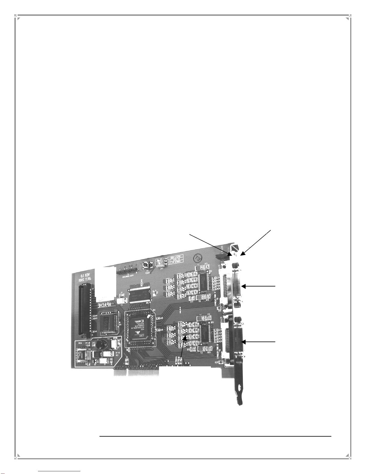
LED Indicators: The ISG Image Grabber board features two LEDs
(one Red and one Green), which can be used to monitor the status of the
board. These LEDs are located at the I/O bracket level of the board. The
green LED indicates the board controller is functioning properly. The
Red LED indicates an image transfer is in progress.
Hardware Installation
Before you install your board, some precautionary measures must be
taken. Turn off the power to the computer and its peripherals, and
discharge static electricity from your body (by touching a metal part of the
computer chassis) before handling any boards. Then, follow the
following steps:
a. Remove the cover from your computer using the
instructions from your computer manual.
b. Carefully position the ISG PCI Image Grabber board in
the selected PCI slot of your computer. Once perfectly
aligned with the empty slot, press the board firmly but
carefully into the connector. Refer to your PC manual
for detailed instructions on how-to-install a PCI daughter
card.
c. Fasten the I/O bracket of the ISG Image Grabber
board to the computer chassis. Follow your PC How to
Install a PCI daughter Card instruction in your PC user
manual.
Copyright 2003 Imaging Solutions Group of New York, Inc., All Rights Reserved
Subject to Change Without Notice

5
d. Replace the cover of your computer.
e. Connect the CameraLinkTM cable to the ISG Imager
Modules Video Connector, J3, and the ISG Image
Grabber connector “A”
f. Turn on your computer.
In some cases, when you boot your computer, Windows’
Plug-and-Play system will detect a new PCI card and you
will be asked to assign a driver to it. At this point, you
should click on Cancel because the driver will be installed
during the installation of the ISG Image Grabber software.
Software Installation
Please refer to the Software Installation Guide for detailed information.
PCI 5V slot
CameraLinkTM
“A”
connector
CameraLinkTM
“B”
connector
Red LED
“LineActive”
Green LED “FPGA OK”
Copyright 2003 Imaging Solutions Group of New York, Inc., All Rights Reserved
Subject to Change Without Notice

6
CameraLinkTM Connector (“A” or “B”)
This Board-to-cable connector supports CameraLinkTM Base
Configuration Industry Standard Interface. It is a 26-position SMT
connector with two Screw Locks (One at each side of the connector) to
tightly secure a CameraLinkTM cable.
§CameraLinkTM Connector part number: 3M 10226 –1A10VE
§Screw Lock part number: 3M 3341-13
Recommended CameraLinkTM Cable:
§1 Meter length: 3M 14B26-5ZLB-100-OLC
§2 Meters length: 3M 14B26-5ZLB-200-OLC
§3 Meters length: 3M14B26-5ZLB-300-OLC
§4.5 Meters length: 3M14B26-5ZLB-450-OLC
§5 Meters length: 3M 14B26-5ZLB-500-OLC
CameraLinkTM Connector Front View
1
14
13
26
Copyright 2003 Imaging Solutions Group of New York, Inc., All Rights Reserved
Subject to Change Without Notice

7
CameraLinkTM Connector Pin assignments
Imager
Connector Frame Grabber
Connector Signal Name
Cable Name
11Inner Shield Inner Shield
14 14 Inner Shield Inner Shield
225 X0-PAIR1-
15 12 X0+ PAIR1+
324 X1-PAIR2-
16 11 X1+ PARI2+
423 X2-PAIR3-
17 10 X2+ PAIR3+
522 XCLK-PAIR4-
18 9XCLK+ PAIR4+
621 X3-PAIR5-
19 8X3+ PAIR5+
720 SerTC+ PAIR6+
20 7SerTC-PAIR6-
819 SerTFG-PAIR7-
21 6SerTFG+ PAIR7+
918 CC1-PAIR8-
22 5CC1+ PAIR8+
10 17 CC2+ PAIR9+
23 4CC2-PAIR9-
11 16 CC3-PAIR10-
24 3CC3+ PAIR10+
12 15 CC4+ PAIR11+
25 2CC4-PAIR11-
13 13 Inner Shield Inner Shield
26 26 Inner Shield Inner Shield
Camera Link ™ is a registered trademark of PULNiX America, Inc.
Copyright 2003 Imaging Solutions Group of New York, Inc., All Rights Reserved
Subject to Change Without Notice
This manual suits for next models
1
Table of contents