Bill of Materials for the Fort Processor circuit, designed by Isn'tses http://isntses.co.uk
Component number/name as marked
on PCB: Qty: Value: Notes:
Resistors + Pots:
We used metal film resistors but carbon would work fine. Ideally get small resistors, the holes are 5.08
mm apart. Larger ones will work but might have to stick up a bit
R1,R2 21k
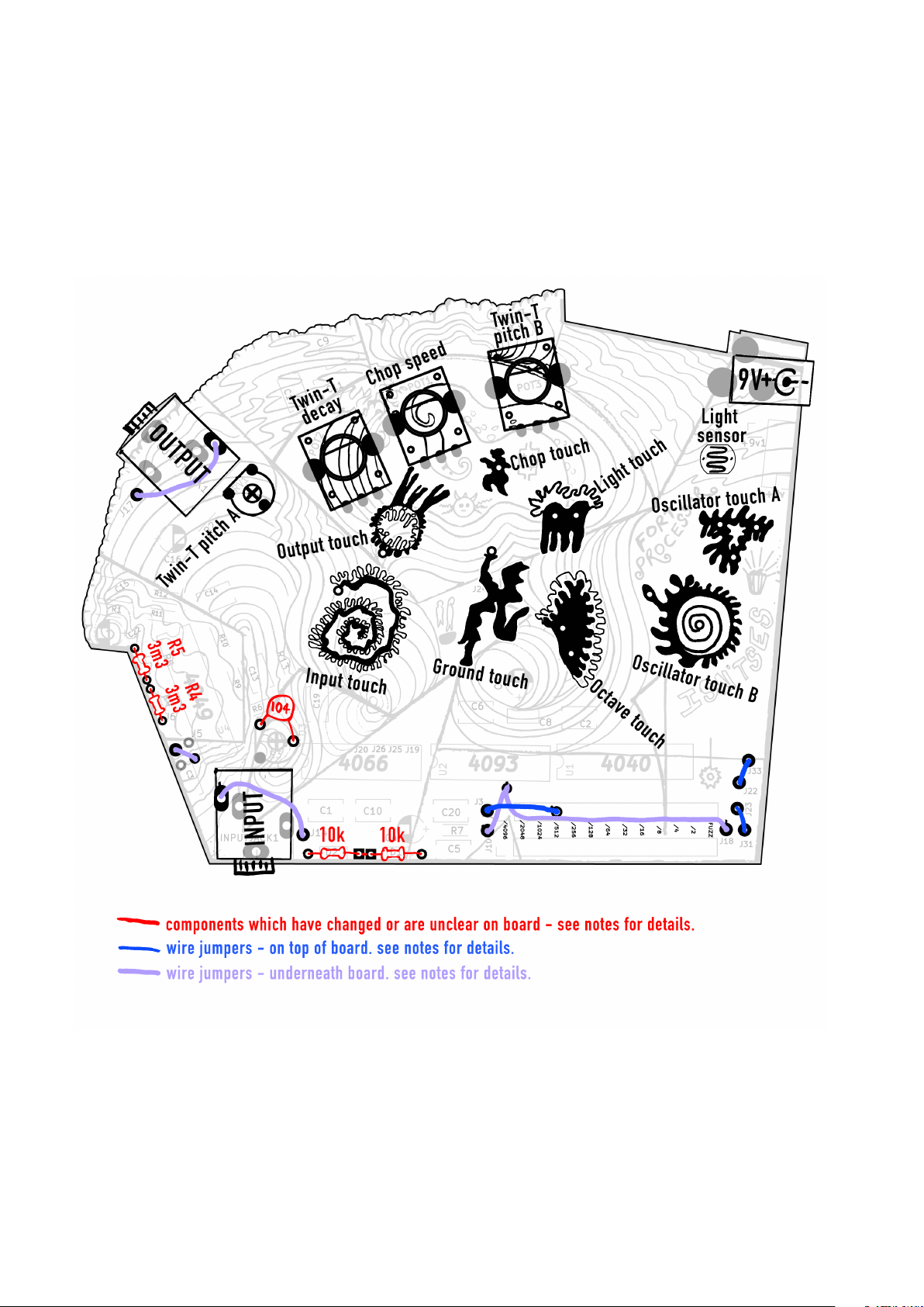
R4,R5 23m3 NOTE: Not clearly numbered! These two go on the edge of the board next to the 4049 IC. See diagram
R10,R11 247k (These are the 2 resistors which mix the oscillator signal with the octave-distorted input signal)
R7 110M
R8 1LDR03 Light dependent resistor
R9,R6 2100k
R12 1470k
R13 12.2k
You could use sockets for 'FUZZ' and all the octave divisions (labelled /1 thru /4096 on the board) to
experiment with different resistors, diodes, pots, LDRs etc connected across the two rows of holes on
either side of the numbers
FUZZ 110k 10k resistor (for mixing the distorted input signal with the 4040 octave divisions)
/2 11k 1k resistor (for CD4040 octave mixing)
/4 11k 1k resistor (for CD4040 octave mixing)
D1, D2 210k NOTE: these are actually 10k resistors, not diodes as marked on the board!
RV1 1trimmer potentiometer 100k trimmer (or experiment other values for a different range.)
POT1,POT2, POT3, 3100k potentiometer
Alps RK09K series vertical 9mm pcb-mount pot or similar. We used "Bourns PTV09A-4020U-B104, 6 mm
Dia. Shaft, 100k" (or experiment other values for a different range.)
Capacitors
R3 1100nF ceramic cap
NOTE: R3 has been changed to a cap instead of trimmer pot! the cap goes in place of the 2 legs
furthest from the input jack, see diagram
C1,C2,C3,C5,C6,C9,C10,C11,C12,C14,
C15,C19,C20 13 100nF (AKA 0.1uF) 100nF Ceramic (Marked 104) or poly fllm capacitor
C4 14.7uF Electrolytic capacitor
C7,C16 21uF Electrolytic capacitor
C22 1100uF Electrolytic capacitor
C8 147nF Ceramic (Marked 473) or poly film capacitor
C13 110nF (AKA 0.01uF) 10nF Ceramic capacitor (Marked 103)
C17 1220nF (AKA 0.22uF) 220nF ceramic disc - Marked 224
IC chips
Use sockets for all ICs. Listed below are the specific ICs we used, but other versions should work work so
long as they still have "CD4xxx" in the names
2DIP-14 sockets chip holder, 14 pins
2DIP-16 sockets chip holder, 16 pins
U1 - 4040 1CD4040BE 12-stage Binary Counter CD4040 - this octave-divides the distorted input signal. 16 legs.
U2 - 4093 1CMOS Quad 2-Input NAND Schmitt Triggers CD4093 - used as 3 oscillators, 1 inverter. 14 legs.
U3 - 4066 1CD4066BE, Analogue Switch Quad SPST 4066 - Rapidly switches between the oscillators and distorted input for chopping/ring-mod fx. 14 legs
U4 - 4049 1CD4049UBE, Hex, CMOS Inverter 4049 - Distorts the input, mixes signals, also used for the Twin-T drum/filter section. 14 legs
Connectors
INPUTJACK1,OUTPUTJACK1 23.5mm switched stereo jack
NOTE: AUDIO WILL BE IN RIGHT CHANNEL ONLY unless bridged with wire jumpers as detailed below.
The jack we used was "Decelect Forgos 3.5 mm PCB Mount Stereo Jack Mfr. Part No. IES101-4"
DC POWER JACK 1DC Power Socket WR-DC Series, 3.5mm Right Angle (or a 9v battery clip: red wire to +9v, black wire to GND)
Jumper wires
NOTE: A few wire jumpers are essential to connect points which were left optional on the PCB, or
changed because the circuit mutated. See notes below and diagram.
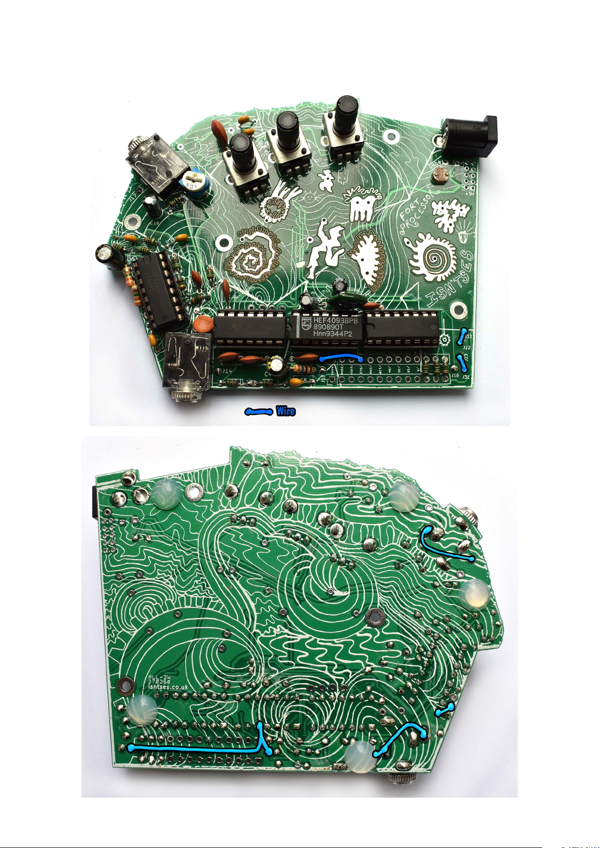
Wire jumper J22-J33 wire (cut-off resistor leg)
on top of board (spare 4066 input A - must be wired to ground, unless used for modifications to the
circuit)
Wire jumper J23-J31 wire (cut-off resistor leg)
on top of board (spare 4066 input B - must be wired to ground, unless used for modifications to the
circuit)
Wire Jumper J18 to pin 5 of CD4093 shielded wire
underneath the board (J18 = the clock input for 4066 ringmod/chopper. Could be modulated by some
other squarewave source for different effects.)
Wire Jumper J10 to pin 5 of CD4093 wire (cut-off resistor leg) underneath the board
Wire jumper J5 to gnd wire (cut-off resistor leg)
underneath the board - from J5, diagonally to pin 8 of 4049 (gnd) (Spare 4049 inverter input - must be
wired to ground unless used for modifications to the circuit)
Wire jumper J3 to '/512' output of CD4040 shielded wire
on top of board from J3 to the hole to the left of '/512' - NOTE: you can experiment with connecting J3 to
other octaves: Bigger numbers = slower. Around /512 it's rhythmical. Below /32 it acts more like a filter
than a drum/oscillator
Wire jumper J14 to Left channel of Input jack wire (cut-off resistor leg)
underneath the board - With this jumper, left and right inputs are summed to mono. Without, right channel
only. NOTE: Mono 3.5mm cables will not work; you need stereo, or stereo to dual-mono
Wire jumper J17 to Left channel of Output jack wire (cut-off resistor leg)
underneath the board - With this jumper, left and right outputs are summed to mono. Without, right
channel only. NOTE: Mono 3.5mm cables will not work; you need stereo, or dual-mono to stereo
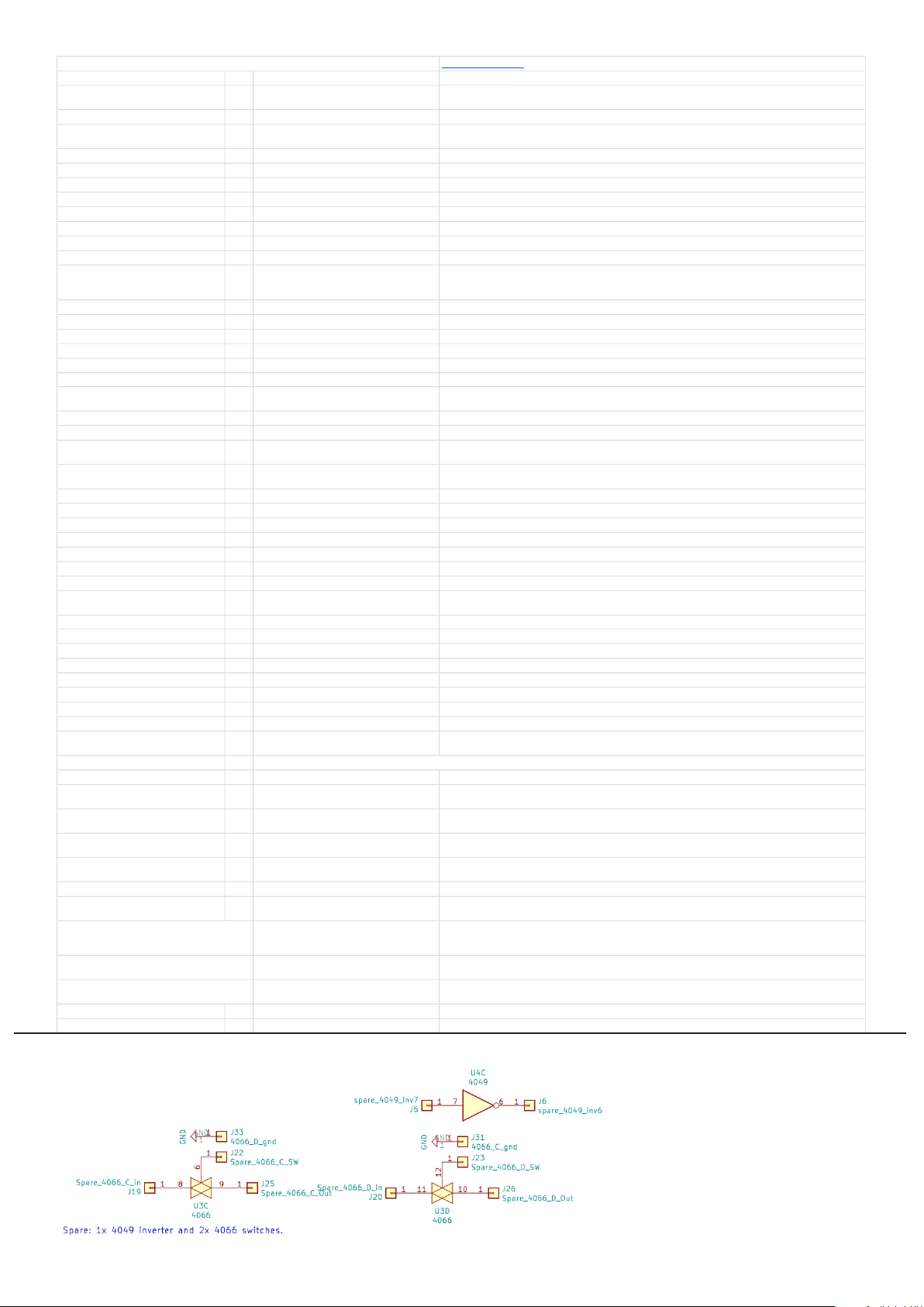
Info on the unused CMOS gates, these are usually safely connected to ground by 3 of the wire jumpers listed above. Ignore this
diagram unless you are doing advanced modications: