Jaton PowerPro VX User manual

PowerPro VX
Pentium Main Board
UserManual


i
Table of Contents
CHAPTER 1 INTRODUCTION 1
¬SPECIFICATIONS 2
-LAYOUTDIAGRAM 4
®SYSTEM BLOCK DIAGRAM 5
CHAPTER 2 MAIN BOARD INSTALLATION 6
¬EXTERNALCONNECTORS 7
-JUMPERSAND SWITCHES 10
®CPU INSTALLATION 11
¯MEMORY MODULE INSTALLATION 13
CHAPTER 3 SYSTEM BIOS 15
¬CPU SOFTMENU™ 17
-STANDARD CMOSSETUP MENU 22
®BIOSFEATURES SETUP MENU 24
¯CHIPSETFEATURES SETUP MENU 29
°POWER MANAGEMENT SETUP MENU 31
±PCI &ONBOARDI/O SETUP 35
²LOAD BIOSDEFAULTS 38
³LOAD SETUP DEFAULTS 38
´PASSWORD SETTING 38
µIDEHDDAUTO DETECTION 39
APPENDIX A QUICK INSTALLATION 1
APPENDIX B INTEL PENTIUM CPUS 1
APPENDIX C AMD-K5 CPUS 1
APPENDIX D CYRIX 6X86 CPUS 1
APPENDIX E HDD INSTALLATION 1
APPENDIX F TECHNICAL SUPPORT 1

ii
APPENDIX G FLASH BIOSUPGRADE 1

Introduction
1
Chapter 1 Introduction
The PowerPro VX have been especially designed for file server, workstation and
professional users. It can support a wide range of processors, including all up-to-date
Intel Pentium processors, AMD K5/K6 processors, and as well as Cyrix
6x86/6x86L/6x86MX processors. It also takes into account, as much as possible, all
futureCPUs.
The PowerPro VX uses SOFT MENU™ technology, which means that all the
processor‘s parameters can be configured without using DIP switches or hardware
jumpers. The configuration is entirely achieved through a “Soft Switch” that allows the
user to set CPU speed and operating voltage with ease.
The PowerPro VX uses Intel 430VX series chip set with 512K Level-2 Pipeline
Burst SRAM on board. Two 168-pin DIMMslots meet the requirements for all memory
configurations required by higher level computing. The 168-pin DIMM slots support
fast page DRAM, EDO DRAM, and SDRAMfor next generation 64-bit systems.
The PowerPro VX also provides two Universal Serial Bus (USB) ports and meets
the Concurrent PCI Rev. 2.1 standard. It also supports IDE interface for Fast HDD
(Mode 0~4) and IDE BusMaster. These featuresalso meet present and futureinterface
standards and needs.
System BIOS features include Plug-and-Play (PnP), Advanced Power
Management, as well as PowerPro VX’s unique CPU operating frequency and voltage
setup featurein orderto meet modern computing demands.

Chapter 1
2
SPECIFICATIONS
1. Jumperless CPU setup with “SOFT MENU™”
⚫Setup of the mainboard’s CPU frequency and voltage without jumpers or
DIP switches.
⚫Softwarereside in system BIOS ROM.
⚫Modification of CPU operating voltage and frequency directly on screen.
2. Versatile CPU support with ZIF Socket 7
⚫Switching type voltage regulator for a more stable CPU operation.
⚫Supports 50, 55, 60, 66 MHz bus clock and as well as 75/83MHz bus clock
reserved.
⚫Supports IntelPentiumCPUs: 100MHz to 200MHz and Pentium with
MMX processors from 166MHz to 233MHz.
⚫Supports AMD-K5™ CPUs: PR 75 to PR 133/ PR 166, AMD-K6™
CPUs: PR 166 to PR 200 and PR 233
⚫Supports Cyrix 6x86™ CPUs: P120+, P133+, P150+, P166+, and 6x86MX
⚫Reserved circuitry to support futureCPUs
3. Chipset
⚫Intel430VX chipset
⚫Supports standard version PCI 2.1
4. L2 Cache Memory
⚫Built-in 512K Pipeline Burst SRAMcache memory
5. System DRAM
⚫Two168-pin DIMM sockets can support FP, EDO and Synchronous

Introduction
3
DRAM (SDRAM) forup to 128MB memory size.
6. System BIOS
⚫AWARD BIOS
⚫Built-in user-friendly SOFT-Menu to set all CPU parameters.
⚫Supports Plug-and-Play (PnP)
7. Multi I/O features
⚫Built-in two Universal Serial Bus (USB) ports
⚫Two fast IDE channels (PIO mode 0~4, Bus Master) supporting four IDE
devices
⚫One EPP/ECP parallel port and two16550 serial ports
⚫Two floppy disk drive connectors (FDD) (360K, 720K, 1.2M, 1.44M and
2.88M)
8. Other features
⚫Standard ATarchitecture dimensions (223mm x 190mm)
⚫Three ISA bus slots and three PCI bus slots
⚫Supports two bootable hard disks to run two different operating systems
Note: All brand names and trademarks are the property of their respective owners.

Chapter 1
4
LAYOUT DIAGRAM
Fig 1-1 PowerPro Layout diagram ©1997, Jaton Corp.
Jaton Power Pro VX
Pentium AT Main Board
PCIset
82438VX
KB BIOS,
RTC,etc.
ISA 1
ISA 2
ISA 3
PCI3
PCI2
PCI1
JP3: Normal: Jumper on 1-2
Clear CMOS: Short 2-3
DIMM 2
DIMM 1
CPU
ZIF
Socket 7
CacheCache
IDE2 IDE1
FDC
PCIset
82438VX
1
40
21
40
2
34
12
-
Power LED
+
RESET
-
IDE LED
+
+
KeyLock
SMI
+
+
Speaker
-
USB
Ports
J
4J
5
Pin 1
Pin 4
CN3 Serial 1
CN4 Serial 2
19
LPT
Key-
Board
Connector
J1 Power
PS/2 Mouse
Pin 1
VR1
VR2
55VRM1
1
BIOS
Battery
Intel
PCIset
82371SB
1 32
Intel
PCIset
82437VX
U23
U19
U22
U3
U9
U4
U27 U28
U1
U5
U14
U
1
9
P9
P8
19
816
1
1 5

Introduction
5
SYSTEM BLOCK DIAGRAM
Fig. 1-2 System block diagram
Pentium Processor
3.3v
Cache
(SRAM)
TAG
Main
Memory
(DRAM)
82371SB
(PIIX3)
CD ROM &
Hard Disk
USB
1
USB
2
PCIDevice(s)
ISA Device(s)
IT8680
Serial Ports Parallel Port
FDC
Host Bus
Tag Ctrl
TIO[0..7]
Address
Control
Control
Control
Address
Data
Address/Data
PCIBUS
ISA BUS
Universal Serial Bus
Fast
IDE
Control
Second Level
Cache
TDX
PS/2 Mouse
PLINK DATA
TXD Control
82437VX
(TVX)
KeyBoard

Chapter 2
6
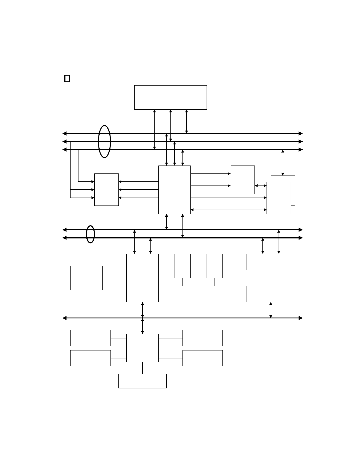
Chapter 2 Main Board Installation
This PowerPro VX main board not only provides all standard equipment forclassic
personal computers, but also provides great flexibility for meeting future upgrade
demands. This chapter will introduce step by step all the standard equipment and will
also present, as completely as possible future upgrade capabilities. This main board is
able to support all IntelPentium including P54C , P55C , Cyrix 6x86, 6x86L, 6x86MX
and AMD-K5, K6 processors now on the market. (For details, see specifications in
Chapter 1.) However, we cannot guarantee that the description given in this manual on
thecircuitry of your main board will workforprocessors not listed in Chapter1. Please
be informed forfurther information about future CPU support.
This chapter is organized according the following features:
Standard externalconnectors
Jumpers and switches
Presentation and Installing of the CPU.
Installing the system memory.
Beforeproceedingwiththe installation
⚫Noteto use a power supply that is for AT since this main board is of AT form
factor.
⚫Beforeinstalling the main board or making any hardware modification, be
sure either the mechanical switch of AT power supply is turn off or the electric
power cord is unplugged to avoid any electrical damages to the hardware.
User friendlyinstructions
Our objective is to enable the novice computer user to perform the
installation by themselves. We have attempted to write this
document in a very clear, concise and descriptive manner to help
overcome any obstacles you may face during installation. Please
take time to read this manual thoroughly.

Main Board Installation
7
EXTERNAL CONNECTORS
In order to connect external devices to the main board, several cables and plugs
have to be connected to proper connectors located on the main board. Pay close
attentionto the orientation of the cables and the position of thefirst pin of theconnector.
PN1 - Keylock and Power LED connector
This connector allow you to connect the Keylock switch and Power LED
indicator from your case to the connector (PN1) on the main board.
Pin number
Name or significance of signal
1
+5VDC [ Power LED]
2
No connection
3
Ground [Power LED]
4
Keyboard inhibit Signal
5
Ground
The “Keylock”is used to lock the computer’s keyboard. When you lock the
keyboard from your computer’s switch panel, the computer keyboard will not function
unless it is unlocked using the key or disconnect the Keylock switch.
PN1 - HD-LED (HDD LED) connector
This connector allow you to connect the two-thread IDE LED connector cable
from caseto the main board PN1 pin 7 (anode)and 8 (cathode). The IDELED will light
up when thehard diskdrive is accessed.
PN1 - Speaker connector
This connector allow you to connect your PC Speaker to the Main Board.
Pin number
Name or significance of signal
9
Sound Signal
10
Ground
11
Ground
12
+5VDC
PN1 - SMI (Hardware Suspend) switch
There is no specific orientation. Connect the two-thread hardwaresuspend plug to the
PN1 pin 13 and 14. This feature is usually not supported by case manufacture.

Chapter 2
8
Pin number
Name or significance of the signal
13
+3VDC
14
Suspend
PN1 - REST (Hardware Reset) switch
There is no specific orientation. Connect the two-thread hardware reset cable to the
PN1 connector pins on the main board.
Pin number
Name or significance of signal
15
Hardware reset signal
16
Ground
J1 - AT Power connector
These have a specific orientation. The three warning marks indicate that if you make a
mistake in pin number or connection orientation, you could destroy your equipment.
During installation, you just need to connect to the correct pins and in the correct
orientation, and to connect connector of the power supply unit to the connector on the
main board.
Pin
number
Name of thesignal or
signification
Pin
number
Name of thesignal or
signification
1
Power Good Signal
7
Ground
2
+5V
8
Ground
3
+12V
9
-5V
4
-12V
10
+5V
5
Ground
11
+5V
6
Ground
12
+5V
I/O Interface
Mouse - PS/2 Mouse connector
There is a 5-pin PS/2 mouse port on the main board. Connect the PS/2 Mouse
connector (included) to the main board. Notice the pin-2 on the 5-pin header does not
have any wire. The PS/2 mouse mini-din connector has an orientation pin. Match the
PS/2 Mouse connector with the mini-din port and plug it in.

Main Board Installation
9
Pin number on board
Name of the signal or signification
1
Mouse data
2
No connection
3
Ground
4
+5VDC
5
Mouse clock
The “PS/2 Mouse Port”is different fromCOM1 or COM2 serial port to which
you can also connect a Mouse. If you do not have a PS/2 Mouse, you can use a serial
mouse and connect it to COM1 or COM2 port.
Keyboard - Keyboard Connector
This connector has an orientation pin. Match and plug your keyboard connector to the
connector on the main board.
Pin number
Name of the signal or signification
1
Keyboard data
2
No connection
3
Ground
4
+5VDC
5
Ground
6
Keyboard clock
LPT- Parallel port connector
There is a 26-pin connector onboard to connect a 25-pin D-shaped female connector
for connecting an External Parallel device to your computer. You may want to change
your parallel port setting in BIOS setup to tune up the performance. Refer to Chapter 3
for details.
CN3 and CN4 - Serial Port Connectors
There are two 10-pin connectors on board to connect two 9-pin D-shaped (DB-9)
male connectors for connecting External Serial Devices to your computer. You may
need tochange thePort settingsin BIOS Setup if you have a Non-Plug and Play device
installed on the main board, such as a internal Non-PnP modem. The CN3is set toserial
port 1 or COM 1 with I/O address 3F8h and the CN4 is set to serial port 2 or COM 2
address2F8h. Pleas refer to Chapter 3 for details.
J4, J5 USB Universal Serial Bus connectors
There are two 4-pin headers on board to connect two standard USB device

Chapter 2
10
connectors (not provided)for connecting External USB devices.
J4 Pin Number
Description
J5 Pin Number
Description
1
Vcc
1
Vcc
2
SBD0-
2
SBD1
3
SBD0+
3
SBD1
4
Ground
4
Ground
Hard Disk and Floppy Disk Controllers
Connector name
Pin number
Name of the peripheral
connected
IDE 1
40
IDE Channel 1 (Primary)
IDE 2
40
IDE Channel 2 (Secondary)
FDC
34
Floppy Disk connector
JUMPERS AND SWITCHES
JP3 : Delete the contents of the CMOS
This jumper is set on pins 1 and 2 at the factory default. This jumper is used
for clearing BIOS setupdata in CMOS when you experience difficulties. For
instance:
⚫You have forgotten the password you set.
⚫You have inappropriately setupthe BIOS, and the system become
unstable.
⚫You want to change the flash BIOS to a different version.
First turn off the powerswitch or unplug the power core to your PC and open
the computer cover, then locate the CCMOS jumper (near the Lithium
battery) and replace the jumper on pins 2 and 3 for a couple of seconds, then
put the jumper back to operation position Pin 1 and 2 to erase theCMOS.
After you have deleted the CMOS information, you need to go back to the
BIOS Setup menu, and reset all the items correctly, such as, CPU, date, hour,

Main Board Installation
11
FDD and HDD parameters, and etc.
CPU INSTALLATION
Jumperless CPU Configuration Main board
You donot need to setup any jumpers or switches on the PowerPro VX main board
for CPU.
Most other main boards require you setup a bunch of jumpers or DIP switches for
the type of the CPU you plan to install. Installing a CPU is becoming more and more
complex since there are so many different kind of CPU brands and models available in
theCPU market place. Not so with PowerPro VX main board. The PowerPro VX main
board simplified the CPUinstallation procedure by eliminating all thejumpers forCPU.
The CPU can be easily setup by software. After you have inserted the CPU into the ZIF
(Zero Insertion Force) CPU socket, and you have installed necessary display interface
card, you can simply turn the computer on. The only thing you will need to do next is
to enter BIOS SETUP to configure the CPU speed and certain CPU parameters in the
CPUSOFT MENU™ . Youmay setup the CPUwhich is not listed withcustom setting.
It reserved several circuits in order to be able to support future processors. However,
we must clarify that “we have only tested the CPUs listed in Chapter 1”, we cannot
guarantee that this board will be able to support future products, because we cannot
forecast future developments.
Related terminology :
External clock
Also referred to as the external CPU clock, or “Bus clock”, it is the input clock of
the CPU. For instance, Intel Pentium P90, P120 and P150 all have a 60MHz
external CPU clock, but have different internal clock multiplier factors.

Chapter 2
12
Clock multiplier factor
The real operation clock within the CPU is the multiple of the external clock. We
refer to this factoras the clock multiplier factor. The four factorspossible are 1.5,
2, 2.5 and 3. The factor differs from one CPU to another. For instance, the Intel
Pentium 166 CPU has a 66MHz external clock, with a multiplier factor of 2.5, so
that the speed of the internal clock is 66MHz x 2.5.
Internal clock
Also referred to as the real internal CPU clock, it is the actual internal operating
clock of the CPU. The Internal Clock is a multiple of the external clock and of the
clock multiplier factor. For instance, the Intel Pentium 90 CPU has a 60MHz
external clock and its clock multiplier factor is 1.5; the Intel Pentium P133 CPU
has a 66MHz external clock and its clock multiplier factoris 2.
Internal CPU clock = clock multiplier factor * external CPU clock
AT Bus clock
Also referred to as ISA SPEED, or AT CLOCK, oreven ISA Bus clock. Ten years
ago, the original specification of AT Bus clock installed in the first generation
PC/AT computers was8MHz, thismeans thatthere are some interface cards which
can only work at 8MHz. In order to guarantee compatibility with older hardware,
we still support 8MHz AT Bus clock, but if your interface card is newer or faster,
you can choose a higher speed for the AT Bus clock, in order to increase the
transmission rate of the interface cards. But we recommend you not to be too
ambitious. An 8MHz setup ensures maximum compatibility.
CPU Voltage - Vcore and Vio
From the voltage point of view, 586 series CPU can bedivided into twocategories:
Single Voltage CPU and Dual Voltage CPUs. Single voltage CPUs include: Intel
Pentium P54C series, AMD-K5 and Cyrix 6x86, etc.
Dual voltage CPUs include: Intel P55C with MMX, future AMD CPUs, Cyrix
6x86L and M2.
Dual voltage CPUs requires two different voltages for the power source: Core
Voltage (Vcore) and IO Voltage (Vio). Vcore provides all the power for internal
processing, and its power consumption is quite important. Vio provides the power
necessary for theexternal interface of the CPU.
P-Rating
The P-Rating is defined by some CPU manufacturers other than Intel to rate the
performance of their CPU in comparison with Intel Pentium CPUs. For instance,
Cyrix 6x86 P166+ has a higher actual speed compared with Intel Pentium P166,
and its internal clock need only be 133MHz versus 166MHz for Intel’s product.
The internal architecture is different betweenCyrix 6x86 and IntelPentium CPU
even they are treated as the same type.

Main Board Installation
13
Having read the related terminology above, please refer to Appendices B, C or D for
more information of your CPU. We suggest you make a noteof the specification of your
CPU, which will help you to configure your CPU correctly.
CPU Settings: CPU SOFTMENU
To configure the speed and the voltage of the CPU, you must enter to the CPU SOFT
MENU in BIOS Setup, which is discussed in Chapter 3 System BIOS.
MEMORY MODULE INSTALLATION
When this main board was designed, we not only have taken into account the
economy and compatibility, but we also focused on the tremendous performance gain
by using SDRAM DIMM.
There are two 168-pin DIMM sockets on board. You may install up to two single
sided DIMMson board. A total of 128MB system memory is supported.
The installation is easy. Simply push the two clips on the DIMM socket ends
outward, orientates the notches on the DIMM against the socket keys, and gently push
it down. Gradually increase the force you use, and make sure the clips are properly
snapped on the module. However, before you proceed with installation, be patient, first
following information carefully:
1. 168-pin DIMM modules specifications
According to the standards defined by JEDEC, thereare different types of
specifications for 168-pin DIMM sockets. Here are thepossible types:
•3.3V UNBUFFERED DIMM
•3.3V BUFFERED DIMM
•5V UNBUFFERED DIMM
•5V BUFFERED DIMM
Currently, the standard forPC is 3.3V UNBUFFERED DIMM, which is used by
this motherboard.
Since the connection between the socket and module is crucial, purchase quality
DIMMfrom a reliable source. The DIMM module board must have a thickness
of 1.270.1 mm. The Gold coating on the DIMM “Gold Fingers” must have a
thickness of 3 to5 micron.
2. 60ns FastPage Mode or EDODRAMDIMMs
If your memory modules are faster than 70ns, say 60ns or 45ns, you can modify

Chapter 2
14
the BIOS settingsto speed up the operating speed of the system.
If you set the external CPU clock at 66MHz or more, we recommend you use 60ns
or even fasterDRAMmodules.
3. Memory error check and correction
The Intel430VX chip set used on this main board doesnot support this feature,
since the memory error check and correction feature may not be effective,and
since you cannot easily find memory modules with memory check and
correction.
4. Memory modules size supported
1Mbitx64 [8MByte], 2Mx64 [16MB], 4Mx64 [32Mb], 8Mx64 [32MB], or
16Mx64 [128MB].
5. Both single sided and double sided memory modules can be used.
6. There are two 168-pin DIMM sockets on the board: DIMM1 and 2. Please
insert theDIMMin ascending order. Notethe DIMM 1 and DIMM2 sockets
can support either single sided or double sided memory modules without any
limitation.

System BIOS
15
Chapter 3 System BIOS
The System BIOS is a program located on a Read-Only Memory (ROM) or Flash
ROM chip on the main board.This program will not be lost when you turn the computer
off.It is the primary channel for the hardware circuit to communicate with the operating
system. Its main function is to manage the setup of the main board and parameters of
interface cards. It setup simple parameters such as time, date, hard disk drive, as well as
more complex parameters such as hardware synchronization, device operating mode,
and also include special features such as CPU SOFT MENU™to setup CPU voltage
and speed and store them in CMOS memory. The system BIOS configuration is one of
the key factorfor your computer system stability and performance.
When the computer powers up, theSystem BIOS program takes the control of the
computer system. The BIOS first run an auto-diagnostic routine for all the necessary
hardware, configures the parameters of the hardware synchronization, and detects all
the hardware. Only when these tasks are completed does it give up control of the
computer to the program of the next level, which is the Operating System.
Afterthe BIOS has achieved the auto-diagnostic and auto-detection operations, it
will display the following message:
PRESS CTRL-ALT-ESC OR DEL KEY TOENTER SETUP
Three to five seconds afterthe message is displayed, if you press the Del key, or if
you press simultaneously the Ctrl Alt Esc keys, you will access the BIOS Setup
Change the parameters in BIOS with caution
The parameters inside the BIOSare used to setup the hardwaresynchronization
or the device operating mode. If the parameters are not setup correctly, the
computer may perform poorly and sometimes may not boot up at all. We
recommend that you donot change the parameters inside the BIOS unless you
are familiar with them. If you are not able to boot your computer anymore,
please refer to the section “Erase CMOS data”in Chapter 2.

Chapter 3
16
menu. At that moment, the BIOS will display the following message:
Fig 3 BIOS Setup main menu
In the BIOS Setup main menu of Figure 3, you can see several options. We will
explain these options stepby step in the following pages of this chapter, but let us first
see a short description of the function keys you may use here:
⚫Press Esc to quit the BIOS Setup.
⚫Press (up, down,left,right) to choose, in themain menu, theoption you want
to confirm or to modify.
⚫Press F10 when you have completed the setup of BIOS parameters to save
these parameters and to exit the BIOS Setup menu.
⚫Press Page Up/Page Down or +/- keys when you want to modify the BIOS
parameters for the active option.
CMOS DATA
What is the CMOS?The CMOS referred here is a memory chip used
to store the custom BIOS configuration information, such as, Hard
Drive type, custom CPU setting, and etc. This memory device has to
be powered by a battery to maintain its content. When the CMOS
battery is out of power and the computer is not powered for a period
of time, or it has been shorted somehow, you may lose thedata stored
in CMOS. Therefore, we recommend that you write down all the
custom parameters of your hardware, and save it to a safe place.
Table of contents
Other Jaton Motherboard manuals