Jaton BX Pentium II User manual

BX Pentium®II Mainboard
User’s Manual
Version 1.00
Copyright © 1998 Jaton Corporation

2
INTRODUCTION
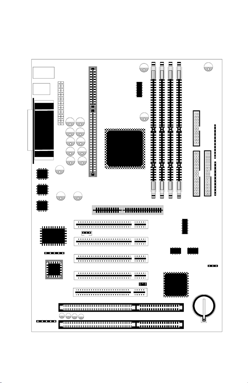
This mainboardisdesignedforthe newgenerationCPU.It supportsthe Intel
CPU SLOT1 (Pentium®II), up to 512MBof memory,superI/O, and Green
PC functions.The mainboardprovideshighperformance forthe server
system and meetsthe requirementsof thedesktopsystem for multimedia in
the future.
This mainboardbased onthe new 440BX chipsetwhich revolutionizesthe
way Pentium®IIPCs use memorybyemployinganOpen PageArchitecture,
a new memoryarchitecture thatlets the CPUaccess main memoryfaster.
Essentially,this meanstheCPU can leave a virtual fingerin up to 32 different
pagesof its memory,makingiteasyforyou to flip back to any of them at any
time.Currently, like a dogged A-to-Z readerof the encyclopedia,a Pentium II
can onlykeepits memoryopento onepageat a time.The CPU usespages
of memoryin a similarmannertopeople leafing through reference works.It
wants to flip backand forthbetweena particularset of pagesat a time.
Flippingrightto them instead of taking that extra microsecond tofindthem
makesthe wholePCruns faster.
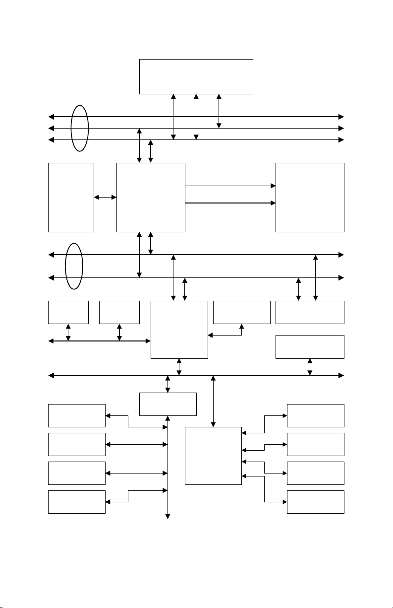
Anotherimprovementinthe chipsethelpsthe CPU whenit findsa single-bit
error while reading error-correctingmemory(thatis, onebit in a byte of
information isincorrect).With the 440BX, the errorcan be correctedon the
fly, withthe correctionwritten back into memory.Current Pentium® IIs can’t
write the correction back.
However,this mainboardoffersmoreobviousimprovements.Most
importantly,supportforthe faster system bus willhave a profound effecton
performance.
But other performance benefitsaccrue formainstreamdesktopsaswell.The
mostobviousof these is support for2x AGP. This meanstheAGP bus is
clocked twice as fastand Sidebandchannel(aslowersidechannelforcontrol
information)isalso used. CurrentAGP implementations onlyuse a single-
speed main channel andmixcontrolinformation withthe data.
1998 Jaton Corporation, USA

3
Contents
INTRODUCTION...................................................................................................2
SPECIFICATIONS..............................................................................................1
CPU..............................................................................................................2
Chipset.........................................................................................................2
Cache Memory...........................................................................................2
Memory (DRAM)....................................................................................... 2
System BIOS............................................................................................... 3
Multi I/O Functions.................................................................................. 3
Miscellaneous.............................................................................................4
LAYOUT DIAGRAM.........................................................................................5
SYSTEM BLOCK DIAGRAM .........................................................................6
PENTIUM®II CPU INSTALLATION.............................................................7
SYSTEM MEMORY INSTALLATION ........................................................10
MAINBOARD INSTALLATION.....................................................................11
INSTALLING THE MAINBOARD..........................................................................12
STANDARD EXTERNAL CONNECTORS..............................................................12
JUMPERAND SWITCHES.....................................................................................17
INTRODUCTION OF BIOS..............................................................................18
CPU SOFT MANU™ II.......................................................................................20
STANDARD CMOS SETUP MENU.....................................................................24
BIOS FEATURES SETUP MENU...................................................................25
CHIPSET FEATURES SETUP MENU....................................................................30
POWER MANAGEMENT SETUP MENU..............................................................31

4
PCI &ONBOARD I/O SETUP..............................................................................35
LOAD BIOS DEFAULTS......................................................................................39
LOAD SETUP DEFAULTS.....................................................................................39
PASSWORD SETTING...........................................................................................39
IDE HDD AUTO DETECTION............................................................................40
INSTALLATION ..................................................................................................40
HOW TO INSTALL THE ULTRA DMA/33 DRIVE...............................................41
INSTALL PCI BRIDGE DRIVER FOR 440BX......................................................42
TECHNICAL SUPPORT....................................................................................44

1
SPECIFICATIONS

2
CPU
⚫CPU SOFT MENU™II eliminates
the need for jumpers or DIP
switches needed to set CPU
parameters
⚫Employs switching type regulators to
stabilize CPU operation
⚫Supports 66MHz and 100MHz CPU
external clock speeds
⚫Supports Pentium® II 350~400MHz
processorcartridge (Based on100
MHz) and Pentium® II 233~333MHz
processorcartridge (Based on 66 MHz).
Chipset
⚫Intel 440BX chipset (82443BX and
82371EB)
⚫Supports Ultra DMA/33 IDE protocol
⚫Supports Advanced Configuration and
Power Management Interface(ACPI)
⚫Accelerated Graphics Port connector
supports AGP 1x and 2x mode
(Sideband) 3.3V device
Cache
Memory
•Level 1 and Level 2 cache built into Intel
Pentium II processorpackage.
Memory
(DRAM)
•Four 168-pin DIMM sockets support
SDRAM
•Supports up to 512MBytes
•ECC support

3
System BIOS
•AWARD BIOS
•Supports Plug-and-Play (PnP)
•Supports Advanced Configuration
Power Interface (ACPI)
•Supports Desktop Management
Interface (DMI)
•Year 2000 Compliant
Multi I/O
Functions
•Floppy port supports up to 2.88MB, and
3 mode floppy
•Ultra DMA/33 bus master IDE supports
up to 4 IDE devices (Including LS-
120MB floppy drive)
•Built-in Standard/EPP/ECP parallel port
connector
•Two built-in 16550 fast UART
compatibleserial port connectors
•Built-in PS/2 keyboard and PS/2mouse
port connectors
•Built-in standard IrDA TX/RX header
•Two built-in USB connectors

4
Miscellaneous
•ATX form factor
•One AGP slot, FourPCI slots and
Three ISA slots
•Reserved circuitry for LDCM feature
•Hardware monitoring –Included fan
speed, voltages, and system
environment temperature
•Board size: 305 * 245mm
Note: All brand names and trademarks are the property of their
respective owners.
*Above 100/66 MHz bus speed supported but not guaranteed due to
the PCI specs.

5
LAYOUT DIAGRAM
BX Component Locations
USB 1
PS/2 KEYBoard/Mouse
CPU SLOT1
COMM / LPT PORTS
CCOMS 1
1 3
DIMM 1
DIMM 2
DIMM 3
DIMM 4
BIOS
ALi
BAT
PIIX4
ATXPWR
443BX
1
1
IDE 1
IDE 2
1
FDC
PCI 1
PCI 2
PCI 3
PCI 4
PCI 5
ISA 1
ISA 21 5
WOR
Green_LED SPEAKER RST SMI POW-ON HD-LED KEYLOCK
1
1
AGP SLOT
15
IR
2 6
15
4
SB-LINK
WOL 1 3

6
SYSTEM BLOCK DIAGRAM
CPU-SLOT1
PMC
82443BX
Main
Memory
(DRAM)
AGP
SLOT
PIIX4E
83977F
Buffer Serial
LPT
IrDA
KBC
RTC
FLASH BIOS
FDCX BUS
ISA SLOT(s)
PCI SLOT(s)
Control
Address
Data
Address
Control
PCI BUS
USB 1 USB 2
Universal Serial BUS
PCI IDE
HEADER
ISA BUS

7
Pentium®II CPU Installation
1. Mount the two blackplasticpegs onto the mainboard.Thesepegs
willbe usedto attach the fan heatsink supports.Notice that one
hole andthe base of one pegare largerthanthe other holeand
peg base. Push eachpeg intoits holefirmlytothe enduntil you
hear it “ click ” into place.
2. Slide a blackplastic support
onto each end of the fanheat
Retention mechanism
Large peg and hold

8
sink , making sure that the
hole andclip areon the
outside edge of the support .
Slide each support toward the
center of the processoruntil
the supportis securedto the
outside groove of the fan
housing.
Top of Processor
Groove in fan housing

9
3. Slide the clip(A) on each
supporttoward the
processor, exposingthe hole
that will fit the peg on the
mainboard .Pushthe latches
(B) on the processortoward
the center of the processor
until they click into place.
4. Hold the processorso that
the fan shroud is facing
toward the pegs onthe
mainboard.Slidethe
processor( DirectionC ) into
the retentionmechanism and
press evenlyandgently.
Ensure that the pegson the
mainboard slide intothe holes
on the heatsink supportand
that the alignmentnotchin
the processorfits overthe
plug in Slot 1 .
5. Slide the clipson the supports
(D) forward untilthey clickinto
place to holdthe pegs
securely.( Applyslight
pressure on the peg andpush
the peg forwardthe clipwhile
pushingtheclip forward.)
Push the latcheson the
processor(E) outwarduntil
they click intoplacein the
retention mechanism.The
latchesmust be secured for
properelectricalconnectionof
the processor.
Note:
•Installinga heatsink andcoolingfan is necessaryforproperheat
dissipationfrom yourCPU.Failingto install these itemsmay result
in overheating and damage of your CPU.
•Please referto your boxedPentium ®II processorinstallation or
other documentationattachedwithyourCPUfor detailedinstalling
instructions.
A
B
C
D
E

10
System memory Installation
The mainboardprovidesfour168-pin DIMMsites formemoryexpansion..
The DIMM socket supports 1Mx64(8MB),2Mx64(16MB),4Mx64(32MB),
8Mx64(64MB),and16Mx64(128MB)ordoublesidedDIMMmodules.Minimum
memorysize is8MB and maximummemorysize is 512 MB SDRAM. There
are fourMemorymodule socketson the system board.(Total eight banks)In
orderto createa memoryarray,certain rulesmustbe followed.The following
set of rulesallowsfor optimum configurations.
•The memoryarrayis64 or 72 bits wide.(Without parity or with
parity)
•Supportsingle and doubledensityDIMMs.
The followingisthevalid memoryconfiguration:
Bank
Memory Module
Total Memory
Bank0
(DIMM1)
8MB,16MB, 32MB,64MB,128MB
8MB~128MB
Bank1
(DIMM2)
8MB,16MB, 32MB,64MB,128MB
8MB~128MB
Bank3
(DIMM3)
8MB,16MB, 32MB,64MB,128MB
8MB~128MB
Bank4
(DIMM4)
8MB,16MB, 32MB,64MB,128MB
8MB~128MB
Total System Memory
8MB~512MB
* * * This table depicts the addressingrequirementsforeachof the
row/columnorganizationsfor each row size. The SDRAM components
used for the optionsshownin the table are as follows:
Option SDRAM Component Type
1 (8MB) 1M x 16
2 (16MB) 2Mx8 or 2Mx32
3 (32MB) 4Mx16 or 4Mx4 (RegisteredDIMM only)
4 (64MB) 8Mx8
5 (128MB) 16Mx4 (Registered DIMM only)
Note: Both 4Mx4 and 16Mx4SDRAM devicesare supportedin the form of
Registered DIMMs only.2 Bank version of 2Mx32is addressedlike a
2Mx8 device,12 row x 9 column.

11
Supported SDRAM MemoryConfigurations
DRAM
DRAM
DRAM
DRAM
DRAM DIMM
DRAM
MA
DRAM
Size
Type
Tech
Depth
Width
SS
x64
DS
x64
Addressing
Row
Col
Banks
Min
(1 row)
Max
(2 row)
SDRAM
16M
1M
16
1M
2M
Asymmetric
12
8
2
8MB
16MB
2M
8
2M
4M
Asymmetric
12
9
2
16MB
32MB
2M
8
2M
4M
Asymmetric
13
8
2
16MB
32MB
4M
4
4M
8M
Asymmetric
12
10
2
32MB
64MB
4M
4
4M
8M
Asymmetric
14
8
2
32MB
64MB
SDRAM
64M
2M
32
2M
4M
Asymmetric
12
9
2
16MB
32MB
2 Bank
2M
32
2M
4M
Asymmetric
13
8
2
16MB
32MB
4M
16
4M
8M
Asymmetric
12
10
2
32MB
64MB
4M
16
4M
8M
Asymmetric
14
8
2
32MB
64MB
8M
8
8M
16M
Asymmetric
14
9
2
64MB
128MB
16M
4
16M
32M
Asymmetric
14
10
2
128MB
256MB
SDRAM
64M
2M
32
2M
4M
Asymmetric
13
8
4
16MB
32MB
4 Bank
4M
16
4M
8M
Asymmetric
14
8
4
32MB
64MB
8M
8
8M
16M
Asymmetric
14
9
4
64MB
128MB
16M
4
16M
32M
Asymmetric
14
10
4
128MB
256MB
Mainboard Installation
This BX6 mainboard notonlyprovidesall standard equipmentforclassic
personal computers,butalso providesgreat flexibilityformeeting future
upgradedemands.Thischapterwill introducestep by step all the standard
equipmentandwill alsopresent,as completelyaspossible,futureupgrade
capabilities.Thismainboard isable to supportallIntel Pentium II processors
now on the market.
!! WARNING !!
Discharge static electricity by
touching the GROUND such as
metalpartof your case connected
with good power ground before
you handle the electronic circuit
boards.
Before installing the mainboard please be sure toturn off or disconnectthe
powersupplyunit. Before making anymodificationstothe hardware
configurationof the mainboard,the powersupplyto any areasof the mainboard
you plan to modifyshouldbe turned off to avoidunnecessarydamage tothe
hardware.

12
Installing the Mainboard
Our objective is to enablethe novicecomputeruserto perform the
installationbythemselves.We haveattempted to write this documentin
a very clear, concise and descriptive mannertohelp overcomeanyobstacles
you mayfaceduringinstallation.Pleaseread ourinstructionscarefullyand
follow them step-by-step.
Most computercaseswillhave a base on whichthere willbe manymounting
holesthat allowsthe mainboardtobesecurelyattached andat the same
time,prevents short circuits.
There are two ways to attach the mainboardto thebase.
•with spacers
•or with bolts
In principle,the best wayto attach the motherboardiswithbolts,and only if
you are unable to do this should youattach the boardwith spacers. Take a
careful lookat the mainboard andyou will see manymounting holesonit.
Line these holesupwith the mountingholesonthe base.If the holesline up,
and there are screwholesthis meansyou can attach the mainboard with
bolts. If the holeslineup andthere are onlyslots,this means youcan only
attach the mainboardwithspacers.Take the tip of the spacersand insertit
into the slots.
After doingthisto allthe slots, you can slide the mainboard intoposition
alignedwiththe slots.After the mainboardhasbeenpositioned,checkto
makesure everything is OK before puttingthe casing backon.
Note: If the mainboard has mounting holes, but don’t line up with the holes on
the base and their are no slots to attach the spacers, don’t worry, you can still
attach the spacersto the mountingholes.Justcut the spacers(along the
dotted line)(the spacermaybe a little hardso be carefulof ourhands).In this
way youcan still attach the mainboardtothebase withoutworryingabout
short circuits.
Standard External Connectors
Inside the case of any computerseveralcablesandplugshaveto be
connected.These cablesand plugsare usuallyconnected one-by-oneto
connectorslocatedon the mainboard.You needto carefullypay
attentionto anyconnectionorientationthe cablesmayhave and, if any,
notice the position of the first pin of the connector.In the explanations
that follow,we will describe the significance of the firstpin.

13
PN 1 (1-2-3-4-5) keylock and Power LED Connector
Pin Number
Nameorsignificance of signal
1
+5VDC
2
No connection
3
Ground
4
Keylockinhibitsignal
5
Ground
Attach the case’s keylock to the connector.
PN 1(7-8) HDD LED Connector
Pin Number
Nameorsignificance of signal
7
LED power
8
HDDactive
Attach the cable from the case’s HDD LED to this connector.
PN 1(10-11) PowerSwitch
Pin Number
Nameorsignificance of signal
PN 1
PN 2
SMI POW-ON HDD-LED KEYLOCK
POWERLED
SP-LED SPEAKER RST
1
1
++
+

14
10
Ground
11
PowerSwitch signal
PN 1(13-14) Hardware Suspend Switch (SMI Switch)
Pin Number
Nameorsignificance of signal
13
Ground
14
Suspend signal
Attach the cable from the case’s suspend switch (if there is one) to this
switch. Use this switchto enable/disable the powermanagementfunction by
hardware.
PN 2(1-2) HardwareResetConnector
Pin Number
Nameorsignificance of signal
1
Ground
2
Reset input
Attach the cable from the case’s Reset switch to this connector. Press
and hold the reset button for at least one secondto reset the system.
PN 2(4-5-6-7) SpeakerConnector
Pin Number
Nameorsignificance of signal
4
+5VDC
5
Ground
6
Ground
7
Speakerdata
Attach the system speakerto connectorPN2.
PN 2(9-10) Green LED
Pin Number
Nameorsignificance of signal
9
LED Power
10
Green LED Active
MOUSE - PS/2 Mousse Connector
Pin Number
Nameorsignificance of signal
1
Mouse data
2
No connection

15
3
Ground
4
+5VDC
5
Mouse clock
6
No connection
Attach a PS/2 mouse tothis 6-pin Din-connector.
KB - PS/2 Keyboard Connector
Pin Number
Nameorsignificance of signal
1
Keyboard data
2
No connection
3
Ground
4
+5VDC
5
Keyboard clock
6
No connection
Attach a keyboardto this 6-pin Din-connector.
ATX PWR - ATX Power input Connector
Pin Number
Nameorsignificance of signal
1
+3.3V
2
+3.3V
3
Ground
4
+5V
5
Ground
6
+5V
7
Ground
8
Powergood
9
+5V
10
+12V
11
+3.3V
12
-12V
13
Ground
14
On/Off controlsignal
15
Ground
16
Ground
LPT
COM 1 COM 2
USB
KEYBOARD
MOUSE

16
17
Ground
18
-15V
19
+5V
20
+5V
Attach the connectorsfrom the powersupplyto ATX PWR.
Caution:If power supply connectorsare not properly attached to
ATX PWR, the powersupply or add-on cards may be damaged.
I/O port connectors
Name
No. of pins
Description
IDE 1
40
IDE channel 1 connector
IDE 2
40
IDE channel 2 connector
FDC
34
Floppydisk connector
LPT
25
Parallel port
COM 1
9
Serial port COM 1 connector
COM 2
9
Serial port COM 2 connector
USB
8
Universal serialBus
Notes: *IDE1, IDE2 are high performance PCIIDEconnectors. Up to
fourIDE interfacedevicesaresupported.
IR - IR connector(Infrared)
Pin Number
Nameorsignificance of signal
1
+5Vcc
2
No connection
3
IR_RX
4
Ground
5
IR_TX
FAN 1, FAN 2, FAN 3: DC-FAN Power Connector
Pin Number
Nameorsignificance of signal
1
Ground
2
+12V
3
Sense
WOR: Wake On Ring
Pin Number
Nameorsignificance of signal
1
5VSB
Table of contents
Other Jaton Motherboard manuals