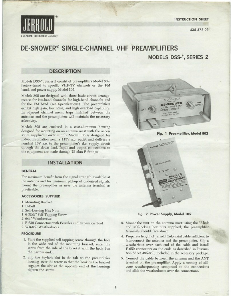
Jerrold SMA Series User manual

-~..:
.. IY
-
.;:,~-
mmtI@ INSTRUCTION SHEET
435-667
a GENERALINSTRUMENTcompany
-'" '"
SOLID-STATE
<I"~~~-~~",,~6-1~N'GLf;.~HANNEL VH F AM PLI FI ERS
... -"
~
"'"
,~
"--
~, . *
'Model SMA..
~U/L./isted
.. "'"
DESCRIPTION
Models SMA-" are high-gain, duaJ-output, strip amwillers
designed for head-ends of master antenna or closed-.circuit
systems, distributing vhf television channels or f.m. sound.
Outstanding features are high overload capability, excel-
lent frequency stability, and low power consumption.
In addition, each amplifier has its own built-in d.c. power
supply with line cord and plug, working directly from a
117 V a.c. outlet. The input circuitry permits the use of
plug-in attenuation pads Models PIP-" for reduction of
the input signal level over a range of 15 dB in 3-dB steps,
in accordance with system requirements. Bridged output
terminals allow interconnection of amplillers directly or
through appropriate mixing networks in order to derive
a common broadband output. Three F-659 cable con-
nectors are shipped with each unit.
The amplifiers are contained in perforated housings for
good ventilation and are designed for vertical installation
side by side on a mounting plate Jerrold Model MP-7.
\
The mounting plate in turn is designed to accept addi-
tional units such as splitters and traps, and can be mounted
on a standard relay rack or installed in an equipment
cabinet.
Models SMA-" are the solid-state advance of the well-
known Jerrold PMA-" tube type series and can be used
not only in new systems but also for expanding or mod-
ernizing existing PMA-" systems, or replacement of indi-
vidual PMA-" units.
INSTALLATION
CN-174
1. Mounting: Each SMA-" ampliller strip is mounted
with two #6 x 1/2 round-head, self-tapping screws
(shipped with the SMA-") on a mounting plate, Jer-
rold Model MP-7. Where a different arrangement is
planne~<L-the "neeessary-mounting hardware will have
to be procured separately.
Model MP-7 will accept eight ampliller strips side-by-
side and a number of accessory units. A typical lay-out
example is given in Fig. 2. Note that the recom-
mended installation method is to mount the strips in
two groups of non-adjacent channels. The strips in
each group can be jumpered directly; the outputs of
the two groups are then combined in a hybrid
mixing network such as Jerrold Model 1596A to .....
Fig. l-Typical SMA.* Strip
=ifF"~ - '=<0'
..
1

... ~
derive a common broadband output for distribution.
Where a more complex head-end equipment requires
additional units and mounting space for them, a
mounting plate Jerrold Model MP-2 designed for that
purpose can be ordered. "'-
INPUTS FROM CUT-TO-CHANNEL ANTENNAS
2411FMIIB 7
/311/0 6'"-
BROAD-BAND OUT
Fig. 2-Typical Multi.Channel Layout
2. Cabling: Mount one of the three F-659:.eoaxial con-
nectors on the input cable, the other two connectors
on the output and jumper cable respectively. Complete
details for the preparation of cable ends and installa-
tion of connectors are given in Jerrold Instruction
Sheet 435-650 enclosed in the accessory package
shipped with each SMA-".
Where only one output terminal on the SMA-" is
used, terminate the second terminal by a Jerrold
Model TR-75F.
Prepare the cables and jumpers for all other SMA-"
strips in the same manner.
3. Signa~ Tests: First connect the line cord and plug of
the S'Mir:" to its associated a.c. outlet. Then connect
a field strength meter (tunable d. voltmeter)-such as
Jerrold Model 720B or 727-to the input cable. Tune
the FSM to the visual carrier frequency of the relevant
tv channel, or to the f.m. channel if such is the case,
and check the signal level in dBmV (see Note below).
If the average input signal level,. plus the specified
amplifier gain exceed the recommended .9utput lev~ ..
replace the factory-mounted Mods!- PIP-O attenuation
plug-in pad on the SMA-" by a pad with a rating that
will reduce the output approximately to the recom-
mended level.
Disconnect the FSM from the input cable and connect
it to one of the SMA-" output terminals; terminate the
other output with a TR-75F. Then connect the input
cable to the input terminal on the SM~" and read the
FSM indication. The output level should be within
::!:1% dB of the recommended level; if it is not, replace
the PIP-" by one that will give the desired result.
Then, as an insurance test, repeat the check on the
second SMA-" output terminal. .
Repeat this procedure for every SMA-" strip instaIled~ ..
Finally, connect all output-cabreS"'and""jumpers t'otheTr
associated terminals on the SMA-" strips and on any
mixing or other networks designed to make up the
head end.
NOTE:
These signal measurements should be taken at inter-
vals throughout at least one 24-hour period so that
fluctuation of signal strength may be noted and the
average signal strength calculated. After initial instal-
lation, additional measurements should be taken at
three-month inter'lfals to determine fluctuations due to
change in seasons.
SPECIFICAnONS
HIGH.BAND LOW-BAND F.M.BAND
PASSBAND 6 MHz, any v.h.f. television channel or t.m. band
GAIN 40dBmin. I40 dBmin. 33 dBmin.
(Levelcontrol by use ot PIP.* plug.in pads)
flATNESS within::!:0.5dB within ::!:0.5dB within::!:1.5dB
OUTPUTCAPABILITY 1.0V(60dBmV)at 1.0V(60dBmV)at 44 dBmV,3 chs.
0.5 dBsyncclip 0.5 dBsyncclip tor-46 dB2A-B
NOISEFIGURE - 10 dBmax. 10 dBmax. 9 dBmax.
TERMINALS: --
IMPEDANCE 75(I 75() 75 (I
INPUT MATCH 16dBmin. ret. loss 16dBmin. ret. loss 10dB(92-108MHz)
OUTPUTMATCH 16 dBmin.ret. loss 16dBmin. ret. loss 16dB(92-108MHz)
INSERTIONlOSS 0.5 dBmax. 0.5 dBmax. 0.5 dBmax.
POWER REQUIREMENT 117 V a.c., 60 Hz, 80 mA, lOW
2
..
'" """=

..- ~
~MAINTENANCE
I""
GENERAL
The solid-state design and low power consumption make
~the SMA-" units virtually maintenance-free. Routine sys-
tem maintenance will consist mainly of periodical checks
of signal levels and on firmness of cable connections.
Should it ever happen that an amplifier becomes inopera-
tive, it is best to replace it by a spare unit so that there
~~~ only a mJn[glUmof interruption in signal distribu-
tion. The faulty- unit can then be returned to Jerrold
where it will be repaired at no charge under warranty
-conditions; otherwise it will be repaired at ~ominal
charge.
Where the user has the necessary instruments and the
skilled personnel for bench-testing and repairing an inop-
erative amplifier, the circuit descriptions, schematic dia-
grams, and replacement parts lists given here will help in
tracing the faulty component.
CAUTION:
An amplifier under test must be equipped with a PIP-O
pad. In no case should the input and output filter compo-
nents be tampered with, nor does the replacement of a
transistor in the amplifier circuitry require a retuning of
tbe frequency-dependent components.
CIRCUITDESCRIPTIONS
A. GENERAL
The SMA-" circuitry consists of:
a. A well-filtered, full-wave rectifier, d.c. power sup-
ply;
b. A tuned-to-channel input filter with plug-in attenu-
Ittioil pad facility;
c. A tuned-to-channel dual output filter;
d. A 3-stage amplifier in the case of low-band and
f.m. channel strips, or a 4-stage amplifier in the
case of high-band channel strips.
Input and output terminals are matched to a 75-ohm
impedance for connection of coaxial cables.
B. LOW-BAND AND FM STRIPS(see Dwg. E863-166)
1. POWER SUPPLY
The d.c. supply consists of line voltage transformer
T4, conventional full-wave rectifier made up of
CRI, CR2, C25 and C26, filter network C20 and
RI4, and smoothing capacitor CI7. This power
supply delivers a -15 V d.c. potential to the
amplifier circuitry and has a 3-wire line cord and
plug for connection to a 117 V a.c. outlet with
ground terminal.
2. INPUT CIRCUITRY
The input signal is applied at terminal JI and is
passed through a pad-plugged in at J2-to a series/
parallel LC network consisting of LI, L2, C3, CI,
---- .... ~"~'I!
~
L3, C4, C2, L4, C5, and L5. This 3-section band-
pass filter is factory-tuned to one of the low-hand
tv channels,> or to the f.m. band, as required by
the user.
3. AMPLIFIER CIRCUITRY
From .the input filter the signal is coupled by C6
to the base of the first amplifier stage Ql. This
and the follo~g stages Q2 and Q3 employ cas-
caded NPN transistQrs arranged in a common-
emitter configuration. Capacitors C9, C12, CI5,
and toroidal transformers TI, T2, and T3 are em-
ployed between stages and at the output for im-
pedance coupling. All three stages have current
feedback, with unbypassed emitter resistors R4
and RS employed in the first and second stage. The
first and third stages also have voltage feedback
from the collectors through resistors R2 and RIO
to the base coupling capacitors C6 and C12 re-
spectively. Base bias is developed across the rele-
vant resistor pairs RI, R3, R6, R7, and Rll, RI2.
Transistor operating stability is achieved by RC
networks in the emitter circuits, namely R5, CS;
R9, Cll; and RI3, CI4 respectively.
4. OUTPUT CIRCUITRY
The output from the collector of Q3 is applied to
a frequency filter consisting of series/parallel LC
network CI5, CIS, L9, CI6, LIO, and CI9. This
filter too is factory-tuned to the required tv chan-
nel or to the f.m. band. From the filter the signal
is coupled through Lll to a signal-splitting circuit
C2I, C22, C23, and C24 from where the two out-
puts are presented at terminals J3 and J4. Capac-
itor C23 is tuned to match the impedances at J3
and J4 to 75 ohms.
C. HIGH-BAND STRIPS (see Dwg. E863-167)
1. POWER SUPPLY
Except for component designations on the sche-
matic circuit diagram, the circuitry of the power
supply and its d.c. output is exactly the same
as that in the low-band/f.m. strips.
2. INPUT CIRCUITRY
The input signal is applied at terminal JI and first
passed through a pad -plugged in at J2 -from
where it goes through a 3-section bandpass filter.
Here too series/parallel LC components are em-
ployed, consisting of LI, L2, C4, C5, CI, L3, C6,
-C7-;-G2,:B4;eS;"€9;"'and C3. This filter is factory-
tuned to the high-band channel specified by the
user.
3. AMPLIFIER CIRCUITRY
From the input filter the signal is coupled through
CIO to the base of the first amplifier stage Ql.
This and the following three stages Q2, Q3, and
Q4 have the same basic circuit configuration as the
amplifier stages in the low-band/f.m. channel
3

.""
strips. Four NPN transistors are employed in a
cascaded common-emitter circuitry. All inter-stages
and the output stage have capacitors andJoroidal
transformers for impedance coupling: TI, .S;,JA;"""-
T2, CIS; T3, C22; and T4, are the components
involved. All stages have current feedback through
R4, R9, RI4, and RI8 respectively. Equally, all
stages have voltage feedba'Ck through RI, RB, Rll,
and R20 respectively. Base bias for each transistor
is developed across the relevant resistor pairs R2,
R3; R7, R8; RI2, RI3; and RIB, RI7. Again, tran-
sistor operating stability is achieved by RC net-
works: Cll, CI2, R5 tor QI; CI5, CI6, RIO for
Q2; CI9, C20, RI5 for Q3; and C23, C24, RI9
'IIfql£..Q4, in the respective emitter circuits.
4. OUTP.DT CIRCUITRY
From the collector of Q4 the output is inductively
coupled through LI7 to a 2"section bandpass Riter
consisting of series/parallel LC networks involving
C27, LI4, C28, C29, and LI5. This Riter too is
factory-tuned to the speciRed high-band channel.
From the RIter the signal is passed through T5 and
LIB which splits the signal energy. equally for
75-ohm impedance dual output presentation at
terminals J3 and J4.
J
.'iF"
ASSEMBLY,SMA-', HIGH-BAND REF. DWG. NO.: E863-167
REPLACEMENTPARTSLIST
REF. DWG. NO.: E863-166
~
ASSEMBLY: SMA-', LOW-BAND AND F.M.
..,--:::
"
..A\
"
4
SCHEMATIC JERROLO
ITEM liES/GNAT/ON QTY. DESCRIPTION PARTNO.
CAPACITORS
1C1,2,28 3prs. Variableplates, assembly 8215-289
2 C3 1 1.5-8.5pF,trimmer 128.572
3 C4 1 18pF,::!:5%,500V 124-079
4C5,7,9, 52-18.5pF,trimmer -128-570'
27,29
5 C6 120 pF,5%, 500V 124.119
6 C8 1 13 pF,5%, 600V 124-115
7 CI0thru25 16 0.02,uF,200V, disc 124.154
8 C30 1 400,uF,16 V, electrolytic 127-123
9C31 1 250,uF,25 V, electrolytic 127.062
CONNECTORS
10 11,3,4 3Chassisfitting Mod.F-61A
11 -3 Cableconnectors Mod.F-659
DIODES
12 CRl,2 2Rectifier,Silicon,CER68A S137.718
RESISTORS,
13 Rl 1 390O,5%, 1,4W 112.099
14 R2,7 21.5kO,5%, 1,4W 112-966
15 R3,8 22.2kO,5%,1,4W 112-932
16 R4 1 100, 5%, 1,4W 112.077
17 R5,17 29100, 5%,1,4W 112-920
18 R6,10,20 33600, 5%, 1,4W 112.098
19 R9 1150, 5%, 1,4W 112-973
20 Rll 1 2000, 5%, 1,4W 112-984
21 R12 1 2 kO,5%,1,4W 112-930
22 R13 11 kO,5%,1,4W 112.977
23 R14 1 12o, 5%, 1,4W 112-079
24 R15 1 300n, 5%, ¥2W 112-293
25 R16 1 6200, 5%,1,4W 112.998
26 R18 1 8.20, 5%,1,4W 112.075
27 R19 1 680, 5%,'12W112-212
28 R21 1620, 5%,2'Vl 112-211
29 R22 11MO,5%,1/2W 112-737
TRANSFORMER
30 T6 1 Linetransformer C141-264
TRANSISTORS
31 Ql 1 A2297 130-220
32 Q2 1 A492 130-185
33 Q3 1 A430 130-240
34 Q4 1 A210 130-200
SCHEMATIC JERROLD
ITEM DESIGNATION QTY. DESCRIPTION PARTNO.
CAPACITORS -
1Cl,2,18 31.5-8.5pF,trimmer 128.572
2C3,4, 5, 55-60 pF,trimmer 128.563
16,19
3C6thru C14 90.02 ,uF,200 V, disc 124-154
4C15 1 2-18.5pF,trimmer .. 128-570
5C17 1 400,uF,16V,electrolytic 127-123
6 C2o 1250JLF,25V,electrolytic 127-062
7C21,22 227pF,5% 124-120
8C23 15-60pF,trimmer 128-563
9 C24 1100pF,20%,1500V 124-101
10 C25,26 21000pF,200V,disc 124-020
CONNECTORS
11 JI,3,4 3Chassisfittings Mod.F-61A
12 -3Cable.fonnectors Mod.F.659
DIODES
13 CRl,2 2Rectifier,Silicon,CER68A S137.718
RESISTORS
14 Rl,6 21.5kO,5%,1,4W 112-966
15 R2 1 8200, 5%, 1,4W 112-976
16 R3,7 22.2kO,5%,1,4W 112-932
17 R4 120o, 5%,1,4W 112.083
18 R5 19100, 5%, 1,4W 1'12.920
19 R8 116o, 5%,1,4W 112.081
20 R9 13600, 5%, 1,4W 112-098
21 RIO 1 680n, 5%, 1,4W 112.105
22 R11 1 2 kn, 5%, 1,4W 112.930
23 R12 11kO,5%,1,4W 112-977
24 R13 1 300n, 5%, ¥2W 112.293
25 R14 1100n, 5%, lW 112-234
"'26 R15 ...!. 1 Mn, o, '12W112-743
TRANSFORMER
27 T4 1 Linetransformer 8141-251
TRANSISTORS
28 Q1 1A2297 130-220
29 Q2 1 A492 130-185
30 Q3 1 A43o 130.240

,
..,.:r., o.,
L
-- -
!"'"
eO
o.
.<
.eo
oi5P
e.
0<
.0
~i5P
.
:;
I' >
c
§I
.g. ;;~
".~ °HI'
= 0
~I
~I
~~Ii
;;
N..
o.~
5
~.;;
j~~
~~~;
~~ H~
~~~~ie
~U~O
0°.0'0
~~H~n
-'"
l";;>
W
0::
t'-
<.D
,
"'
<.D
(1J
W
...
'"
~
I
J

~
I
!
\
!
I
\
I
I
\
If
I
I
\
I
I
.4
-- -----
/
"!~
~
~~~ ~<~
L.- ~~ =c --~;-~#~ .~,
""""
.."."
- ~""""~~
-------
WARRANTY
Each unit of Jerrold Equipment is warranted for 90 days
against original factory imperfections in material and work-
manship.
In the event any unit of equipment should fail in service during
this period, pack the complete defective unit carefully, attach
a letter stating the reasons the unit was believed to be
defective, and return it to our Service Department, Jerrold
Electronics Corp., 15th Street and Lehigh Avenue, Phila., Pac
19132, prepaying transportation charges. It shall be repaired
or replaced at no charge.
Such service 6r repairs as may be necessary as the result of
abuse or accident are not included in the warranty. In the
event of any service breakdowns after the warranty period,
this unit may be returned for repairs at a nominal charge.
-""'"
-<"
I
~I
"'
i\
I
)
I
\
I
\ ~
\~
I
\
\
I
\
I
l
I
~
p~ ~~-
...
!j~
Ijj ,j!
mm
wm
r-"..~
E...--.-
JERROLDELECTRONICSCORPORATION
EDUCATIONAL AND COMMUNICATIONS SYSTEMSDIVISION
Philadelphia, Pac19105
... "
"""
"
?
~~~ ~-
'\
'£0
i!:
~
<:I
J
Publishedbythe JerroldElectronicsCorp.,EngineeringLaboratoryPublicationsDept.
LKEE,12/69 Printed in U.S.A. 435.667 ~@ 8016
.. J
This manual suits for next models
1
Table of contents
Other Jerrold Amplifier manuals
Popular Amplifier manuals by other brands

XFIRE AUDIO
XFIRE AUDIO E-6004D owner's manual
Kenwood
Kenwood KAC-8102D instruction manual

CIE-Group
CIE-Group TD 816 operating instructions
Absolare
Absolare Integrated Amplifier user manual

K&M Analog Designs
K&M Analog Designs Two-Rock Jet Signature owner's manual
OT Bioelettronica
OT Bioelettronica OT-BridgeAmp4 user manual
