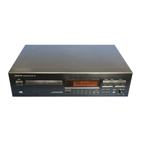
Kenwood DP-3300D User manual

Knob (Button)
(
K29
-251
6
-04)
Phone
jack Knob Knob {Button)
(E11-0127-05) (K29-1641-04) (K27-1514-O4l
Top plate
(A52-0099-02) Panel
ass'y
{A20-501
1-021
Knob (Button)
lK29-25a1-O4lx4 Knob (Buttonl Knob (Button)
(K29-2546-04)x9 (K29-2581-04)x15 lnsu
latJr \
(J02-01
88
-1
5lx4
Phono
jack
(E
13-023O-05)x2
Knob
lK29-2584-o4l Cover Slide
switch
(
F07-0499
-04) (S31
-2094-05)
Slide
switch Power
coardbushing
(s31-2083-05) (J42-0083-051
Phono
jack
(E
13-0130-05) AC Power
coard*
{E30-}
In complicance with Federal Begula-
tions, following are reproductions of
labels on, or inside the product relating
to laser
product safety.
K€NWOOD-Corp. certifies this eguin.
ment conforms to DHHS Regulations
No. 21 CFB 1040. 10, Chapter1, Sub-
chapter J.
DANGER : Lasor r8diltion when opon
and int€rlock dofeatsd.
AVOID DIRECT EXPOSURE
TO BEAM, *Refer
to parts
list
onPage
51
.

1.
2.
4.
Remove
eight screws
db retaining
the sidepanels
to
the chassis,and remove
theside
panels.
Then
remove
sixscrews
@ tixing
thetop
panel
tothe
chassisframe,
andremovethetop
panel.
DISASSEMBLYFOR
HEPAIR
the Mechanism
ass'y
the tray toward
the
Move
the gear
on the leftside
of
with your finger
(@ ) and Putt
tront
(
@ ).
\a@
@
5.
Pullup the four clawson thetray
panel
inthe
direction
of the arrowsand removethe tray panel
by pulling
it
ouT
in
the
ciirection
@ .
Push
the
trayback
( G! )
Disconnectthree
connectors
(CN3,
CN4,CN5)
fromthe
CD
plaver
unit
(X32-1090-11)
(G ).
Remove
four screws
@ retaining
the Mechanismass'y
and removethe Mechanism
ass'yby pulling
it slightly
backward
thenrupward
(GF ).

2
3
5
7
7
7
10
10
12
12
12
12
12
12
12
12
13
13
13
13
16
16
16
17
6-3. Explanationof
functions ...... 14
7. Signal
processor
lG : GX23035
(X32-1090-11
:lC3). 14
7-1. Block
diagram 14
7-2. Explanation
of terminals 15
8. Digital
outputsignal
demodulator
lC : CXDl075P
7
8
9
9
(X32-1090-11
: lC9).
B-1. Block
diagram
B-2. Terminal
connection
diagram
8-3. Explanation
ofterminals 17
...20
21
21
20
20
24
27
4.
5.
E] E] E] E] tr)
I!]E)EElE)
u@gE@
EgUE@
@
t@r
,-l l-t *'
L, L, i.[]
CO
NTENTS/THANSPO
RTATI
O
NSCREW
TRANSPORTATION
SCREW
DISASSEMBLY
FORREPAIR
BLOCK
DIAGRAM
CIRCUIT
DESCRIPTION
1. Description
of components
. .
1-1
. DACUN
rT
(X25-2860-1
1). . . .
1_2.
CONTROL
UNIT
(x29-1780-00).
. ..
1-3. CD
PLAYERUNIT
(X32-1090-11)
..... .
2, Circuitdescription
2-1. DAC
lnterface
circuit
(X25-286O-11)
. . . . .
2-2. Distortion
correction
circuit
lx25=2860-11)....
2-3. Dropout
control
circuit
(X29-1780-00)
DualD Flip-FfoplC : TC74HC74F
(X25-2850-00
: lCl,lC4)
3-1. Blockdiagram
3-2. Truthtable .
HexD Flip-FloplC : TC74HC174F
(X25-2850-00
: lC3)
4-1 . Terminal
connectiondiagram
4-2. Truth
table .
DA Converter
: PCM56P-K
(X25-2860-1
1 z
lCl,lC2l
5-1. Block
diagram/Terminalconnection
li^^-^-
u tout dI l
S-2. ExJtanation
ofterminals
Digitalfifter: SM58O4B
(X25-2860-11
: lC4) . .
6-1. Blockdiagram
6-2. Explanationoftermlnals
TRANSPOBTATIONSCREW
Before
operation,
removethe two redscrews
attached
to the bottom of the unit used
duringtransport
from the
factory.Removeboth screws
usinga coin,etc.and,
after
removing, retain them together with the Warranty
cardand other documents.
Whenthe unit isto be trans-
ported
again,be
sure
replacethetwo screws
to theirorigi-
nal
position.
ATTACHING
THETRANSPORTATION
SCREWS
1.Turnthe
power
ON
withoutloading
disc.
2. Turn OFF the power
after
thedisplay
showsthe
follow-
inqindication.
8-4. Explanation
offunctions
. . .
9. Microcomputer
: PPD75208CW-040
(X32-1090'11
: lCl1)
9-1 . Terminal
connection
diagram
9-2. Explanation
of terminals
. . .
ADJUSTMENT
...
Adjustment
Q6nlrna
I rEgrqgs
Abgleich
Description
of Signal
Waveform,
Connection
of
Measuring
Instruments 30
VOLTAGECHECKTABLE ... 34
Pc
BoARD
(CoMPONENT
slDE
vtEvQ ... . 1? -
pcBoARD(FO|LSIDEVIEW)
..... .... 38
SCHEMATIC
DIAGRAM 41
EXPLODEDVIEW(MECHANISM) ...49
EXPLODEDVIEW(UNIT)
.... 50
PARTSLIST . 51
SPECIFICATIONS
. BACK
COVER
3. Installthetransportationscrews.

CO
NTENTS/THAI\ISPO
RTATI
O
NSCREW
TRANSPORTATION
SCREW
DISASSEMBLY
FOBREPAIR
BLOCK
DIAGRAM
CIBCUIT
DESCRIPTION
1. Description
of components
. .
1-1.
DACUN|T
(X25-2860-11)
....
1_2.
CONTROL
UNIT
(x29-1780-00).
. ..
'r-3.
cD
PLAYERUNIT
(X32-1090-11)
..... .
2. Circuitdescription
2-1. DAClnterface
circuit
(X25-2860-11)
' . . . .
2-2. Dislort"ion
correction
circuit
(x25,2860-1
1
) . . . .
2-3. Dropout
control
circuit
(X29-1780-00)
DualD Ffip-FloplC : TC74HC74F
(X25-2850-00
: lCl,lC4)
3-1. Block
diagram
3-2. Truthtable .
HexD Flip-FloplC : TC74HC174F
(X25-2850-00
: lC3)
4-'l . Terminalconnection
diagram
4-2. Truthtable .
DA Converter
r PCM56P-K
(X25-286O-11
: lCl,lC2)
5-1 . Block
diagram/Terminalconnection
di^^-^-
ulqqldlll
5-2. ExJlanation
oftermrnats
Digitalfifter: SM58O4B
(X25-2860-11
: lC4) . .
6-1. Block
diagram
6-2. Explanationofterminals
TRANSPORTATION SCREW
Refnre nnpr:ti.}n remove the two red scfewsattached
vPv, u!,v',, '
v
to the bottom of the unit used
during
transport
from the
factory.Removeboth screws
usinga coin,
etc.and,after
remoVing,retain them together with the Warranty
cardand other documents.
Whenthe unit isto be trans-
ported
again,be
sure
replacethetwo screwsto theirorigi-
nal
position.
ATTACHINGTHETRANSPORTATION
SCBEWS
1.Turn
the
power
ON
withoutloading
disc.
2. Turn OFF the power
after
thedisplay
showsthe
follow-
inqindication.
8-4. Explanation
offunctions
. . .
9. Microcomputer
: PPD75208CW-040
(X32-1090.11
: lCl1)
9-1 . Terminal
connection
diagram
9-2. Explanation
of terminals
. . .
ADJUSTMENT
...
Adjustment
6-3. Explanationof
functions ...... 14
7. Signal
processor
lC : CX23035
(X32-1090-11
:lC3). 14
7-1. Block
diagram 14
7-2. Exolanation
of terminals 15
8. Digital
outputsignal
demodulator
lC : CXDl075P
2
3
5
7
7
7
7
I
9
9
10
10
(X32-1090-11
: lC9).
B-1. Block
diagram
B-2. Terminal
connection
diagram
8-3. Explanation
of terminals
16
16
16
17
17
...20
21
21
20
20
24
27
3.
4.
5.
12
12
12
12
12
12
12
12
13
13
13
13
P6nlano
I rE9rqgs
Abgleich
Description
of Signal
Waveform,
Connection
of
Measuringlnstruments ...30
VOLTAGECHECKTABLE ... 34
Pc
BOABD
(coMPoNENr
slDE
vtEvQ . .. 1? -
pcBoARD(FO|LSIDEVIEW)
....- .... 38
SCHEMATIC
DIAGRAM 41
EXPLODEDVIEW(MECHANISM) ...49
EXPLODEDVIEW(UNIT)
.... 50
PARTSLIST . 51
SPECIFICATIONS
. BACK
COVER
/^\
((Lr)
\Y/
@
vI
@
fl
U
ElEtElElCt C@
@gltEtrtE) r@r
ID ID IEI E
E0@tD@@ ,-rr-r *^
c;;; L, L, ili.]
3. lnstallthetransportationscrews.

DISASSEMBLY
FORREPAIR
7. Turn the Mechanism
ass'y
upside
down, remove
two
screws
@ tixingthe rod and,
while
lifting
the motor
block
diigonally
upward
((E )' pull
the
pickup
inthe
directionof the
arrow
((D )
8. Whenassembling
the pickup
block,
insertthe chassis
of the Mechanismass'y
in the directionof arrow
@ .
Alignthe position
of thescrewsandsecurethem
( (E ).

BLOCK
DI
ENVELOPE
WAVEDET,
FFIAME
SYNC.
DET.
FRAME
SYNC.
PBO.
TECT
DEINTERLEAVE
TIME
BASE
GENERATION
TIMEBASE
CORRECTOB
SIGNAL
PBOCESSING
SYSTEM
CONTROL
CIRCERROR
CORRECTION
^\-
| 'r' I
| 'v7,
I
-l--
rl
ll F
BUS
INTER"
FACE
E- U
z
U
o
01
(x29-
)
tc1
(cx20108)
r-- OUTPUTIN.
TERFACE
TRACKING
BFIAKE
u-
rcl
(cx20109) (r PDO tc3
(cx23035)
----
^_J-F-
tc5l2t2l,o2l3l3l
TBAY
MOTORDRIVE
GC-
OPEN
CLOSE
NT
JLI
I
,rl
FEED
MOTOB I FEED
I
E_J
@
J
U' FEED DISC TRAY
MOTOR
MOTOR
MOTOR

OCK
OIAG
BAM
:1
TERLEAVE
OAJE
iRATION
BASE
iECTOR
qL
ESSING
EM
'FOL
ERHOR
ECTION
tcs,tc7,
tc9 f
c11,ol,o3 tc13l1l2l
tc7
DIGITAL
DATAINV. lc13-tc21
C
ERROR
IRECTI
HEADPHONE
AMP.
HEADPHONE
AMP.
DIGITAL
OUT
t----.,l'--'w.-6)
-AIBY
qtb I
r-Jl\---a____J
tl
l-
IT
,7v ,ln
tc6,tc8,
lc10 \c12,o2,A4
tcls(2121
ol 1
rc
l1-fllffiej-@
L I-'U
+rh
PH3 010
/v
rc10(1/6)
Q13 ti
t12V
--r- -32V
DATA
INTER.
POLA-
TION DIGITAL
FI
LTER
SOD
A
SID
LINE
OUT(R)
VARIABLE
OUT.
FL DISPLAY

CIRCUIT
DESCRIPTION
1. Description
of components
1-1. DACUNIT
(x25-2860-11)
Component Use/Function Operation/Condition/Compatibility
lcl ,lc2 PCM56P.K D/A converter Convertsdigital
value
into agalog
quantity.
tc3,rc4 NJM5532D.D l-V converter 11/21
: Converts
DAC current input into voltage.
(2121
: Generates
offset voltage{or distortion correction.
tc5-rc10 NJM5532D-D Opamp Forms
a GIC (General
lmpedanceConverterlwith LPF.
tc ,1c12 pPA6SHA Dual
FET Forms
the 1st
stageof output amp.in thefinal stage.
LIJ cx20197 Opamp Amplifier device
of output amp,
a1A SM5804B Digitalfilter Digitalfilter with 4-fold oversampling.
L t3 TC74HCO4F HEX inverter Inverts
the logic
of digitalfilter output anddelays
data.
Lto TA79LO06P 3-terminalreoulator (-) power
for DAC.
c't7 TATSLOO6AP 3-terminalregulator (
+)power
for DAC.
tc 8,tc19 TC74HC74P Dual
D flip-flop Usedin distortioncorrector
circuit
tc20 TC74HC393P Dual4-bit binary counter Usedin distortion
correctorcircuit.
tc21 TC74HCO4P HEX inverler Usedin distortion
correctorcircuit.
PH1 T95-0035-05 Photocoupler Interface
betweendigitalfilter and DAC (Used
for data).
PH2 T95-0036-05 Photocoupler Interfacebetween
DAC and X32 (Emphasis).
PH3 T95-0036-05 Photocoupler Interface
between
DAC and X32 (Muting).
01
-o4 2SC945(A)(O,P) Transistor Used
in cascode
stageof 1
st stage
o.f
output amp.
05.06 25K170(V) FET Begulated
power
supply
for constant-voltage
circuit of ist stage
of output amp.
07,Q8 2SC945(A)(O.P) Tra
nsistor Regulated
power
supply
for differential
amp.of 1st
staqeof output amp.
010 DTCl
14YFF Switch De-emphasis
relavdriver
Q1
1DTC]14YFF Switch Muting relaydriver. 'r
012 DTC114YFF Switch Emphasis
photocoupler
driver.
n1? DTC11
4YFF Switch Muting photocoupler
driver.
014 2SA733(A),(O,P) Switch Usedfor supplyingvoltage
to the photocoupler
output.
D1
.D2 RD5,iJS{B) Zener
diode Suppliespotential to the cascodestageof lst stageof output amp
D3,D4 RD5.1JS(B) Zener
diode Determines
the potential
of constant-current
circuit of differential
amp of 1
ststaqeof output amp.
D5,D6 RDl
OES(B) Zener
diode Feference
power
supply
for constant-voltage
circuit of 1st
stageof
output amp.
D8 tSst/u Switch Protects IC1
6 a
ga
inst counte
r-withstan-d
i
ngvol
taqe.
D10,D11 tsSt/t) Switch Usedfor countermeasure
against
staticelectricity.
D12.D13 iSS133
or1SS176 Switch Usedfor short-circuiting
counter-electromotive
voltaqe
of relav.
ut4 RDl
OES(B} Zener
diode Determines
the operatingvoltage
of transistor
SW014
Litc 1
SS1
76 Switch Protects
lC1
7 againstcounter-withstanding
voltage.
Table1-1
l-,
a(
t:
t
ji
1-2. CONTBOL
UN|T
(X29-1780-00)
Component Use/Function Operatiory'Cond
ition/Compatibil
ity
tcl cx20109 Optical
pickup preamp. Focusing
error
signal
generation,
trackingerror
signal
generation,
RF
signal
generation
and phase
compensation,auto-symmetry correction
ci
rcuit.
tc20/21 M5218P Trackingerror polarity detector When
tracking
error
is
(
+ ) :+4V output.
When
(-) :-4V output.
tc2l2l2l M5218P Flaw
detectorlevelcomparator Normally : -4V output. When flaw isdetected : + 5V output.
ILJ pPD4053BC Trackingerror
signal
selectswitch
The error signalsupplied to the tracking servocircuit isselected
accord-
ingto the logic
of the MIRR signalsupplied
via
pin 11.
When
MIRR is
"L" : Normal
trackingerror
signal.
When
MIRR is
"H" : Constantvoltage
at + 0.5V or -0.5V.
The polarity of the constant voltage
supplied when the Ml RR signal
is"H" isselectedaccordingto the tracking error polarity detector
output suppliedvia
pin 1O.
When
"H" : + 0.5V. When
"L" : -0.5V.
Theerror
signalsuppliedto the tracking
servocircuit isdetermined
accordingto the polarity of the flaw detector output supplied via pin 6.
When
"L" : Errorsignalis
suppliedto the tracking
servocircuit.
When
"H": Error
signalisnot supplied
to the tracking
servo
circuit.
Table1-2 7

1-3. CD
PLAYER
UNIT
(X32'1090'11)
CIRCUIT
DESCRIPTION
012\
: PLL
compensator
circuit
l2l2l : CLY
compensator
circuit
Generates
search
pulses
for focusing servo,
tracking servo
and feed m
servo.
Generates
microprocessorreset
pulse.
EFM decoder,
correction/intetpolut!9n
citcuit, PLL cit'
Signal
processor
RAM (16K). (LPF
+ amP.1.
(LPF + level
shifter).
11l2J
: CLV
compensator
silsui{
(amp.)'
l2l2l :TraY
driver
circuit
Digital
datainverter
circuit.
Controls
digital
signal
supply
to DAc'
Converts
digital
audio
datainto Sony/Philips
digital l/O foimat to g'
transmission
signal
lC9 demodulation amp,
pulse
transformer
driver'
Controls
disPlaY,
key-inPut and
servo
lC.
Interface
circuit
between
microprocessor
9!ql! if:919y
+5Vresulated
voltase
fora449lel9-!!!-!i!91
-5V requlated
voltage
for digital
and PLL lines'
+ 5V regula'ted
voltagefor servoline.
Error
amp
oI x12Vconstant regulated
circuitfor DAC'
Digital
datainverter
circuit
For loqic
inversion
usi -disital
SW.
Current
buffer for tracking
actuator,
feed
motor andtray motor or
ci
rcu
itrv.
Used
to prevent operation of eye-pattern center sampling circuit w
thedisc
motor is
not driven'
inversion
and
level
shifting
of MONortp,4-|1on'
9I?9991
lnverts
digital
data
at highspeed
andamplifies
the current'
Discharges
-5V DAC
unit
to 0V.
Supplies
-5V to DAC
unit
An
emitter-follower
used
for
supplying
+5Vto DAC
unit'
Controts
SWs
Q6
and
07
Controls potential at base
of Q8'
Eliminates
offset
of motor
driver
circuit
while
me19!l1l99q9d'
Turns
-5V for laser ON/OFF
Power
supply in the constant-voltage
regulated
laser
powersupply
Gomponenl Use/Function Operation/Condition/Compatibility
Goes
"H" whena signal
is
output from the pickup'
Detects
the + side
envelope
of RF signal.
(Small
time constant)
Detects
the + sideenvelope
of RF signal.
(Largetime constant)
When lC2l2l2l output becomes
-4V, the switches
function to
vent the negative
potential to be applied to pin 6 of lC3'
When lC2ll/21 output becomes
-4V, the switches
function to
ventthe negative
potentialto be applied
to pin 10of lC3'
Whenthe flaw detector level
goes
"H" by detecting aflaw, the
turns
the
MIBR signal
also
"H".
atl 25C945(A)(o,P) FOK
current
buffer
a2 2SC945(A)(o,P) RF siqnal
enveloPed
detector
o3 2Sc945(A)(o,P) RF siqnal
enveloped
deteclor
Dl ,D2 1SS176
or
1SS131 Switch
D3,D4 1SS176
or
'l
SS131 Switch
D5 1SS176
or
1SS131 Switch
Table
1-2
M51
951ASL
cxK581
6M
TCT4HCOOP AND gate
(switch)
TC74HC08P Digitaloutput signal
modulator lC
cxDl
075P
withstanding
buff.
rc12-lC'l
53-terminal
3-terminal
regulator
TC74HC74P
Current
amPl
ifier
transistor
STA341
M
Di
gital
transistor
switch
Dioital
transistor
switch
DTA1
24EN
2SC1923(R,O)
2SA733(A)(O,P)
2SC945(A),(O,P)
2SA992(F,E)
2SC1845(E,F
)
25K246(Y,G
R
)
2SA733(A)(O,P)
25K246(Y,G
R
)
Table
1-3

($
rs CIRCUIT
BESCHIPTION
Component Use/Function Operation/Condition/Compatibility
o14 2SC945(A)(O.P) Ripple
filter Transistor
ripple
filterfor constant-voltage
regulated
VDD supplycircuit
forFLdrivers
lCs
(lC12to
lClb).
ut3 2SA1
286 Ripplefilter Transistor
ripplefilterfor constant-voltage
laser
power
supply
circuit.
Cl z>L5240 Current
buffer Current
buffer
for
disc
motordriver
circuit.
72SA1286 Current
buffer Current
buffer
fordisc
motor
drivercircuit.
o25C945(A)(O,P) Switch Inverts
the logic
of pre-digital
SW.
019 2SA733(A)(O,P) Switch Connects
rhe low muting potential
in DAC unit to GND.
o20 2SC945(A)(O,P) Switch Control
SW
used
to set
r12V regulated
DAC
unit
power
to tOV.
421 2S,A1286 Currentbuffer Current
buffer
forfocus
actuator
driver
circuit.
422 2SD1
266 Current
buffer Current
buffer
for focus
actuator
driver
circuit-
o23 z>u Izoo Bipple
filter Transistor
ripple
filterfor
+ 12Vregulated
DAC
unit
powersupply
circuit.
o24 258941
(P) Ripple
filter Transistor
ripplefilter
lor
-12V regulated
DACunit
power
supplycircuit
D,I rJJt/o Switch Preiigital SW.
D2 1
SS176 Switch Diode
SWusedfor keyscanning
in testmode.
D3 1
SSl76 Switch Time-constant
SW
for quick discharge
ot C4E.
D4 1
SS176 Switch Used
to prevent
variation
of MUTE and EMpH digital
audio
data
during
searching,
etc.
D5 RD6.8ES(82) Zener
diode Provides
reference
potential for constant-voltage
regutated
V6p supply
circuit
for FL driver
lCs
(1C12
to lC15).
D6,D7 DSM1A1 Rectif
ierdiodes Used
for voltage
multiplyinS
rectifier.
D8 RD8.2ES(B) Zener
diode Usedto maintainFL dispay erase
potential
no 1
SS176 Switch Diode
SWused
to interrupt
optical
output
while
the
digital
output
sw isoFF.
OFF.
Dl0 BD2.7ES(B} Switch Used
todecrease
r12V DAC
power
quickly
when
power
isturned
OFF.
Dl1 RD6.2JS(82) Zener
diode Provides
reference
potential
for r12V regulated
DAC power
supply
circuit.
Dl
2-Di
5rJJ |/O Switch Diode
SWusedfor countermeasure
against
static
electricity
in digital
output.
D1
6.D17 1
SS1
76 Switch Qiode
usedfor countermeasure
against
staticelectricity.
D1
8-D20 1
SS176 Switch Diode
SW
connected
to limir SW.
D21 RD5.6ES(82) Zener
diode Provides
reference
potential for -5V laser
oower.
D22 1B4841 Bectif
ierdiode fiectifier diode
bridge
for servo
anddigital
lines.
D23 1B4B'41 Fectifierdiode Rectifier
diode
bridge
for DAC line.
D24 1
SV147 Vari-cap Vari-cap
in VCO circuit of PLL.
Table1-3
2. Circuit
description
2-1. DAC
Interface
circuit
(X25-2860-11)
The digital
line
andanalog
line
of the Dp-3300D
are
separated
by transmitting
DAC digital
audio
data
using
photocouplers.
Although
thephotocouplers
are
of thehigh_
speed
type,
the photocoupler
outputs
stiliinclude
atime
lag of approx.
20ns.
To compensate
for this delay,
an
inverter
isused
with BCK
and
two inverters
are
used
with
176.5kH2
usedfor LATCH
signal.
tc14
(Digital
filter)
DAC
to DATA (Lch}
DAC
to DATA (Rch)
DAC
tO BCK
DAC
to LATCH
Ftu
FIJ'
r;
$Bi
;v
T
Fig.2-1 DACInterface
circuit

CIRCUIT
DESCRIPTION
2-2. Distortioncorrection
circuit
(X25-2860-11)
In Fig.
2-2, D-FF1,
D-FF2,
BC1and BC2
form the
circuit which extractsthe data logic
of the digitalaudio
data's
1sth bit whichis immediately
after
the MSB,and
delaysthe logic
by DATA. For the detailsof the opera-
tion,
please
refertothetiming
chartin Fig.2-3.
The DAC hasbeendesignedto acceptthe connection
of the circuitwhichcompensates
for theerror
of the cur-
rent valuecorrespondingto the value
of the MSB.The
circuit
consists
of semi-fixed
resistorVR1 and
resistorsR1
to R3.
OP1 is usedto add/subtract
the currentcompensating
the error
correspondingto the value
of the 15thOitto/
from the D/A converted
current. Therefore,
when the
currentcorrespondingto the 1sth bit is outputfrom the
DAC accordingto the logic
of the 15th bit, the current
passes
throughOPi sothat the errorcorrespondingto the
valueof the 1sth bit is
eliminated.lf the currentcorres-
ponding
to the 1sth bit is
notoutput
from
theDAC,
the
Fig.2-2 Distortioncorrection
circuit
output from OP1becomes
0V, sothat the compensation
currentisnot appliedto theD/A converted
currentoutput
from
theDAC.
CLK
4.2336
MHz
DATA
LATCH
176.4kH2
(n-1)th DATA {n)th
DATA
C DATA
15losic
[(n-1]thl DATA
15logic
[(n
+ 1)th]
D X DATA
1slosic
t(n-1
)thl X DATA
15tosic
[(n]thl I \
Fig.2-3 Timingchartof distortion
coruection
circuit
2-3. Dropoutcontroller
circuit
(X29-1780-00)
With conventional
servosystems,tracking
errorsignal
TEfrom pin 17
TE of CX2O'I
89areoutputdirectlyat
pin
i of CN3.However,
with the DP-3300D,
thewaveformof
TE is shaped,
the shapeof waveform
TE varieswhile it
passes
throughlC3. Theoperations
andwaveformsin this
process
areas
follows.
DATA
15
logic
[(n
+ 1)th]
n;r fE
rcgl f
@
IE
Fig.
2-4 Dropoutcontrollercircuit
10

is
$o In case
of thedisc
containsscratch:
lf the disccontainsa scratch
asshownin Fig.2-5(al
,
the RF signal
maylackthepositive
side
envelope.02 and
03 havedifferent
time constants,but theyareboth used
for tracking
the positive
envelope.When
thesignal
with a
largetime constantisdividedby R15
andR16,thesignal
waveformbecomesasshownbythedottedline
in Fig.
2-5
(b).
Withsignalsthat have
a smalltimeconstant,thewave-
form becomesas
shownbythesolidline
in
thesame
figure.
Therefore,
at the point of the scratch.the levelshown
by the solid
line
dropsbelowthe level
shown
bythedotted
line,
and
theoutput
trom lC2(212)
pin
7 will beinverted.

(Fig.2-5(c))
Thissignal
is
shapedby D1andD2,andappliedto lC3
pin
6.WhenlC3
pin
6goes
"H", lC3setstheSWto OPEN,
andVR4 andR24
set
TEto GNDlevelsothatthetracking
error
signal
doesnot go to the next
stage.
Thismeansthat
TE is0V only
while
"H" isappliedto lC3
pin
6,andthe
waveformasshonwin Fig. 2-5(e) is output as
TE from
CN3
pin
1
. "H" level
is
alsoappliedto MIRR
via
D3atthis
period.
However,asthe controlof lC3
pin
6 has
priority
overit. TE of CN3
goes
GND level
regardless
of thevaria-
tionofMIRR.
o In caseof the disc
envelope
lacks
lower
side
(when
only
focusing
servo
isused
intestmode,
etc.):
As
shownin Fig.
2-6(a),
when
there
isnotvariation
in
the positive
sideenvelope
of the RF signal,
thestatusof
lC3 pin 6 remains
"L" and the SW iskept
conductive.
When
the RF
signal
lackslower-side
envelope,
theMIRR
signal
goes
"H" and,
asa result,
the
SWcontrolled
by lC3
pin 11 ischangedfrom
pin
'l
2,
which
isthe
TE
signal
input
from CX20109,
to pin
13.Pin
13is
applied
with
aconstant
voltage
of + 0.5Vor -0.5V fromtheSW
controlled
by lC3
pin 10. The polarity
of the constant
voltage,
+ 0.5Vor
-0.5V, is determined
by the signalfrom lC2(112ir.
(Fig.
2-6(b)to (e))
Therefore,
when
theMIRR
signal
goes
"H", thepolari-
ty of the trackingerror
signal
from CX20l09 isdetected.
When
the polarity
is positive,
a voltage
of + 0.bV is
applied
to lC3 pin 13 via
pin 15,
and
outputfrom lC3
pin 14.When
it isnegative,
avolgage
of -0.5V is
output
fromlC3
pin
14via
the
samerouting.
When
theMIRR
signalrerurns
Lo
"L",lC3 pin I4 out-
puts
theTE
signalfrom
CX20109.
(Fig.
2-6(f),
(S))
C!RCUIT
DESCRIPTICIIU
RFO
OV
o2
emitter
tc2l2l2l
pin 7 output
OV
OV
tc212l2l
pin
7output
RFO
OV
tc2l1l2l
pin
'loutput
OV
{-l +5v
tc3 ll
pinoinput I I (d)
lc3
pin
14output
.
' bvFnHrt*.1*F-{fift}.|r{ilrttlF (e}
?
I
Fis.2-5
(b)
(c)
-4V
(a)
(b)
+4V
(c)
-4V
(s)
F,,
ie-nJ,
","n/v\Y
lC3 t- =
5V
pin
10
input I I (d)
OVa
lC3 t- +
0.5V
Pin
15
outPutu
ffi -o.uu
t"'
MrRRoutput n n n n +5v (rl
l?nt,oou,ou,
A f- tl- /l- /
ovm
:{-; Fis.
2-6
11

CIRCUIT
DESCRIPTION
3.
Duaf
D FliP-FloP
lC:TC74HC74F
(X25-2850-
O0
: lC1'lC4)
d:
\l
4'
\i
3-2. Truth table
4-2. Truth table
Table
3-1
CLR1 Dl CLKT
Fig'
3-1
4.
Hex
D FliP-FloP
lC:TC74HC174F
lX25-285O-00:
lG3)
CLEAR 10 ru Fis'
4-1
5. DAConverter
: PCM56P-K
"' ifisl-iebo-rr
:
lc1,lcz)
5-1 . Block
diagram/
Terminal
connection
diagram
\.
ANALOG OUT
(r3.0vl
3-1. Block
diagram
CLK1 PRl
Fis.
3-1
L
H
H+
L
H
G
O0 : Condition before
inPut
4-1 . Terminal
connection
diagram
vcc 60 6-D P X
Table
4-1
cK-
LEC'
(OAT
Fis.
5-1 12

r3
s^ cf
RculT
0EscRtPTt0tu
6. Digital
filter:SMS804B
(X25-2860-11
: lC4)
6-1. Block
diagram
xI
XT
;-T
cKo
CKSL
lssf
scsL
Table6-1
glElglflrac
oOO@
oooo
No5x
"0L
iq.nf
tii':::
'B;:t
5-2. Explanation
of terminals
Terminal
No. Terminal
name Function Terminal No. Terminal
name Function
1-Vcc Analog negative
power
supply. IVout Voltage
output
2' DIG
GND Digital
ground. 10 HF Feedbackresistor.
+VL Logic
positive
powersupply. tl el Summing
junction
(op
amp.
input)
NC No connection. 12 ANAGND Analog
ground.
CK Clockinput. IJ Iout Current
output.
6LEC Latchenable
control inout. l4 MSB
ADJ MSB
adjustment
terminal.
DATA Datainput. tc V POT Potentiometer terminal.
ILogic negative
power supply to * Vcc Analog
positive
power
supply.
Table
5-1
FlESletBlfitfitEc
Mu!tiplexer/Accumulator
{16x18bit/25bitl
Outpurlslch/Output timin€ CCT.
6-2. Explanation
of terminals
Terminal
No. rerminal
name alo Function
S-two Serial
input modeselect.
SI
EB B ch serialinout enable.r
siEa ,Ach serialinput enable.'
ABCKI ISerial
input bit-clockinput.
5SID ISerialinput data
11 CKSL IERSI = "H" for external
clock
inout.
12 Vss GND
power
supply
terminal
(0V).
XT Clockinput
when
eKSf = "H"
18 POMD POMD
="L" for in-phase
parallel
output mode
19 SOMD SOMD
=
"L" during
serial
output.
tn LSBO
27 SODA oA ch serialdata outout.
28 SODB oB ch serial
dataoutput.
30 BCKO oSerial
output bit-clock
outpur.
co4 OSerial
output control clock4.
44 FdST FOS-L
= "H" for serialoutpurmooe.
45 YOFB TOFB="U" for
2'scomptement
display
outpur
46 VDD Positive
power
supply
terminal (+ 5V).
47 XOFB XOFB
=
"H" for
2'scomplement
display
input.
48 PISL IPISL
= "H" for serial
input mode.
60 LSBI ILSBI= "H" for MSB-first
serialinput.
13
Fis.6-1

6-3. Explanation
of functions
o Basic
configuration
of filter
This LSI makes
it possible
to 4-fold
oversampling
out-
put of both L and R channels
from asingle
chip'
When
the
sampling
frequency
of theinputis
44'1kHz,
the
output
rate
is
176.4kH2.
This LSI incorporates
two stages
of linear-phase
FIR
(non-cyclic)filters
connected
inseries'
The
1st
stage
output
isthe2-foldoversamplingoutput,andthe2ndstageoutput
is
the
4-fold
oversampling
output'
CIRCUIT
DESCRIPTION
Fig.6-2
Fig.
7-1
Fig.6-2 shows
thesimplifieddiagram
of filterconfigu-
ration.
The lst stage
filter (DFl) isan 8O-step
FIR type
filter,and.the
2ndstage
filter (DF2)is
a 15-step
FIR
type
filter. Bothfilters
have
the.2-foldoversampling
function,
so that a total of 4-fold oversampling
output can be ob-
tained.
OUTPUT
176.4kH2
(4-foldover-
sampling)
7.Signal
processorlC: CX23035
(X32-1090-11: lC3)
7-1. Block
diagram
Egs
99I
;NF I's
-t
=o
aa
o6
t003uu'
lSUEuoo
eo9
383,
ERRORDET.
€RROR
CORRECTION
EEEHa
RHgFHsBEEaE
14

CIRCIJIT
DESCRIPITOru
\.
)7-2. Explanation
of terminals
Terminal No. Terminalname vo Function
1FSW oSpindle
motor output filter time constantswitchingoutput.
2MON oSpindlemotor ON/OFF control output.
?MDP oSpindlemotor driveoutput. Rough
speed
control in CLV-Smode,
phase
control in CLV-P mode
4MDS oSpindlemotor driveoutput. Speed
control in CLV-Pmode.
5EFM EFM
signalinputfrom RF amp.
6ASY oEFM signal
slice
levelcontrol output.
7MI
RR IMIBROR
input
fromRFamp.
8vcoo oVCO output. f = 8.6436MH2 when lockedto EFM sional.
vcol VCO
input.
10 TEST tov).
11 PDO oPhase
comparisonoutpu'tbetween
EFM signal
andVCO12.
12 Vss GND
(OV)
tc CLK Serial
datatransferclock input from CPU.Data
islatchedat rising
edge
of clock.
14 V'T Latchinput from CPU.Datafrom B-bitshift register
(serial
data
from CPU) islatchedin each
register.
15 DATA Serial
data input from CPU.
to XRST System
resetinput. Fesetat "L"
CNIN Tracking
pulse
input.
i8 SENSE oOutput of internalstatusin correspondence
to address,
19 MUTG Muting input. When
ATTM of internalregisterA is"L", MUTG : "L" Ior normal
status
and MUTG : "H"
for soundlessstate.
20 CRCF oSubcode
O CRC check
resultoutput
t1 EXCK Clock input for serialsubcodeoutput.
zz SBSO oSerialsubcodeoutput.
23 SUBQ oSubcodeQ output.
SCOR oSubcodesyncSO
+ Sl output.
25 WFCK oWrite Frame
Clockoutput. f = 7.35kHz when frame
syncislocked.
28 GFS oFrame
sync
lock
statusdisplayoutput.
29 DBOS tlo ExternalFAM data
terminal.DATA 8. (MSB).
30 DBOT /o Exlernal
FAM data
terminal.DATA 7.
5t DB06 t/o ExternalBAM data
terminal.DATA 6.
5Z DBOS /o Exlernal
FAM dataterminal.
DATA 5.
33 VDD Power
supplV
(+
5V).
34 DB04 t/o ExternalRAM data
terminal.DATA 4.
35 DBO3 tlo ExternalRAM data
terminal. DATA 3.
JO DB02 t/o External RAM dataterminal. DATA 2.
37 DBOl tlo ExternalRAM dataterminal.DATA 1 (LSB).
38 RAOl oExternal
FAM address
output.ADDROl (LSB).
'39 FA02 nExternalRAM address
output. ADDR02.
40 RAO3 oExternal
RAM addressoutput.ADDR03
41 RA04 oExternalFAM addressoutput. ADDR04.
4Z RAOS oExternalFAM address
output. ADDR05.
FAO6 oExternalRAM addressoutput. ADDR06.
44 RAOT oExternalRAM addressoutput. ADDR07,
FAOS OExternalRAM address
output. ADDR08.
46 BAO9 oExternal
BAMaddress
output.ADDR09.
47 RA1
OoExternalRAM address
output.ADDF10.
48 FlA I I oExternalRAM addressoutput.ADDR1l (MSB).
49 RAWE oWrite Enable
output to external RAM. (Active
when "L")
50 BACS oChipSelectoutput to external RAM. (Active
when "L")
Table7-1
)L
1Tl
t-
r ;';
15

:
f*ut ilffiid"o outP"t =
+'23gonllHt'
GND
(OV). - -
I'.JlIiiu,* inp"'
+
=
e'aoz2MH'' ', ,
c
r*.
"* "\"d"yJ,
-!-,1
*T: r:
::iii
li
;::i:;
iffiilH::;
Terminal No. Terminal name l/o
51 c4M
52 Vss
53 XTA
56 c2PO o
58 SLOB IAudio
9ata
o"lp'] !"]i^ r,:;;i:;;i;;i;;; ;;t;;
;;;;;;i;i o* "*,
"*" to'parutt"'ou*out'
59 A!1i:
oala
oi:P:;Uf' " 1=
"1"
Power
suPPlY
(+
5V)' ffiI.tout when
PSSL
= "L"
70 DA09 n
VDD
-14 DA12 oDA12 outPu NtrNIP rt when PSSL
-
75 DA13 o
76 DA14 n
7A DA1
6oDA16
outpur
80 LRCK o44.1kt12 strooe srgl
CIBCUIT
DESCRIPTION
Table
7-1
Notes) PLCK : YCOt2output' t = 4'3218w{zwhen locked
with EFM signal'
DENL : L CH serial
data
enable
signal'
DENR : R CH serial
data
enable
signat'
8.Digital
output
signal
demodulator
lC : CXD1075P
(X32-1090-11
: lC9)
8-1 . Block
diagram
o
flcsse
C21O: lnverted
dZT-0
o'tPut'
Tzro , Bit
clock
output'
f =2'116BMHz'
DATA : Audio
signal
serial
data
outpur'
t
9x
ii
-f 8-2. Terminal
connection
diagram
BCK
DATA
LRCK
VRDTY
cl0
CFCF
vss
CKSL
EXCK
D1
02
D3
D4
D5
D6
VDD
D7
LSFT
XILR
INVB
I92FS
XTAL
EXTAL
CBSL
RSET
TEST
c9
TX
Fig.8-2
?I
241
231
221
21
20
19
18
17
't6
15
t
2
4
o
6
9
10
I
111
I
112
|13
lra
16
Fig.
8-1

!
\
p
8-4. Explanation
of functions
o Selector
pins
For increased
freedom in the selectionof the signal
processor
LSI
lC,
the
digital
output
signaldemodulatorlC
is
equippedwith various
selectorsthat can
select
theinter-
nal
functions
according
tothe
signal
processor
LSI
lCused.
TEST
(pin'i
7) :Testmodesetting
input.
Fixed
at"L".
RSET
(pin
18)
:When
TESTis
"L", thesignal
demo-
CIRCIUT
DESCRIPTION
Table8-2
LSI lCare
set
bythe
"H" andstops
whenit is"L". When
theLSIisnot
operating,only 192Fsis
output norrnally
while other outputs
are
fixed.
The followingfive pins
aretheselector
pins
whichsets
the
signal
processor
LSI
lC.
)u
eTt
l: The modes
of thesignal
processor
above
methods.
8-3. Explanation
of terminals
Terminal
No. Symbol vo Function
BCK IBit clock input. Connect
the clock which shifts
out data
in theexternaldigitalaudiodataoutput circuit.
DATA Digitalaudiodatainput (NRZ).
LFICK IClock input for L/R channelidentificationof digitalaudiodatainput.
The frequency
is
equal
to Fs(sampling
frequency).
4VRDTY IValidity flag input. "H" flaq isusedwhenthe datais
being
processed
by interpolation,
etc.
5cl0 IC-bitcategorycodeC10 presetting
input.
6LNUT IC-bit
block
start
syncinput.When
CX23035is
used,connectedthisterminal
totheCBCFoutput
(pin
12),
I
nothercases,thesiqnalisfixedat
"H".
7Vss GND.
8CKSL Inputforselectingif thereferenceclock
is
EXTALorits1/3.
YLSFT Input for selectingbetweenLSB firsr and MSB
first operation.
10 XI
LR lnput for selectingbetweenLRCK "H" and "L"
11 INVB lnput for selectingif BCK timing used
isthe riseor fall
12 ts,zrs UClockoutput for useas
CD masterclockwhen CD isconnected.
The frequency
is192timesthe samplingfrequency.
IJ XTAL oWhen
a X'tal oscillatorisused.it is
connectedacrossthis
pin and EXTAL (pin 14)
14 EXTAL When
a X'tal oscillator
is
used,it isconnected
acrossthis pin and XTAL (pin 13). In other cases,this pin
isusedfor external
clock input.
15 TX oOutput of transmissiondataconverted
into the digitalinterface
format.
to C-bit
category
codeC9 presetting
input.
ItrJt Test
modeselectinDut.
Fixed
at "L" in normaloperation.
't
8RSET LSI operation
start/stopinput. "H" duringoperation
IY CBSL Input for selectingif the C-bit input isserial
or parallel.
20 D7 C4 {Emphasis
information) presettinq
input when C-bitinput is
parallel.
21 VDD +5V.
22 UO IC3 (Copy
Inhibitinformation)
presettinq
inputwhenC-bitinputis
parallel.
ZJ D5 C2 (lD1)
presetting
inputwhen
C-bitinput
is
parallel.
.A D4 IC1 (lD0) presetting
input when C-bitinput is
parallel.
Whenit is
serial,usedas
SUBO input which pro-
vides
C1to C4.
25 ISCOR input which indicatesthe startof subcodeblock to be includedin U-bitdata.
26 D2 WFCK input which indicatesthe frameof subcode
to beincluded
in U-bit data.
27 D1 Serial
input for subcode
to beincluded
in U-bitdata.(Connected
to SBSO).
28 EXCK Clock output to besuppliedto the externalsubcodeoutput cirucit in orderto shift subcodeout.
{Connect
EXCK).
Table
8-1
dulator
tsl lCoperateswhenRSET
is
TerminalNo, Symbol Doscription
ICKSL Fixed
at "H" when EXTAL input is384Fs,
"L" when it is128 Fs
LSFT Fixed
at "H" when DATA input isMSB
first,
and "L" when it isLSB
first.
10 XI
LB Fixedat "L" when LBCK inputisL-chand
"H"."H" when
it is
"L"
11 INVB Fixed
at "L" when DATA isshiftedat the fallingedgeof BCK,
"H" when it isshiftedat the risinqedqe.
IY CBSL Fixedat "L" when C-bit input isserial,
"H" when it is
parallel.
17

CIRCUIT
DESCRIPTION
o Input signal
description
(ex,
CX23035)
1) Digiul audio
data
This LSI uses
16-bit
serial
digital
audio
data'
and
the
data bits are arranged
from backward
with respect
to
LRCK.As the period
of clock
BCKisequal
to the data
bit rate,
more
than 16 clocks
are
required
for each
word'
For example,
whenthe signal
processorLSIconnected
is
CX23035,
which
is
a CD
signal
processor,LRCK
is
"H"
during
the L-ch
audio
data
and
"L" during
theR-ch
audio
data,and the audio
datais shifted
in MSB-first
mode
at
the fall of BCK. These
Jactors
canbe setby the above-
mentioned
selector
Pins.
LRCK
DATA
BCK
3) Channel
status
data
By connecting
D2 (pin 26) with thewriteframe
clock
output
terminal
(wFcK) of thecD LSl,
D3 (pin
25)
with
the subcode
sync
S0 + 51 output
terminal
(SCOR)'
D4
lpin 24\with the subcode
O outputterminal
(SUBO)
and
CRCK (pin 6) with the subcode
O error
flagterminal
(CRCF),
it becomes
possible
to read
respectively
the lD0'
iot, COpv lNHlBlTand
EMPHASIS
information
from
SUBOand to setthem on the specified
positions
of the
C-bit
data.
However,
when
there
isno
terminal
correspond-
ing
to
cRCF,
it
shall
be
f
ixed
a|"H"
'
2) Master
clock
When
a 1-sample/48-clock
one-chip
CD lC (CX23035)
is used,a X'tal oscillator
of 3 x 128Fs
= 16'9344MH2
shall be connected
across
XTAL (pin 13) and EXTAL
(pin 14). The internal
circuitray
of this LSI lC uses
the
1/3
clock,
which
is
5.6MHz,
as
the
master
clock'whilethe
CD uses
the output from 192Fs(pin 12) as
the master
clock(3 x 12BFsl2
= 8.4672MH21.
It is also possible
to connect
a 128Fs(5'6448MH2)
X'tal oscillator
across
XTAL and EXTAL and to use
it
as the common master
clock with the signal
processor
LSI.
Fig.8-3
The category
code(subcode
bits9 and 10)isinputin
DC via Cg (pin 16) and CiO (pin
5)' With
the CD'
the
category
code
is (C9,
C10)
= (1' 0) sothe bitsare
fixed
at
C9
= "H" and
C10
= "L"'
Note: D4 (SUBO) is read at the rise of D2 (WFCK)'
latched
and,when CRCF
= "H"' loaded
as
theC'bit
dataat the fall of D3 (SCORI'
lf CRCF
= "L" '
thePrevious
value
is
held'
With this LSl, it is alsopossible
to inputthe chanel
status
data
in parallel.
In this
case'
lDO'
lD1'COPY'
EM-
PHASIS
and category
code
areinput respectively
to D4'
D5,
D6,
D7
and
C9
and
C10
bvdirect
DC
inputs'
WFCK
EXCK
SBSO
18
SYNC.
PATTERN
Fig.
8-4

I
\
3
D3{SCOR}
-rr-r rTr l-r l-rz- rl-r l-r r-r l-r l-
D4(suBol v lp0(1lv
lp1(1)
vcopy(1xEMp(1)\____ X rootzlXrortzlrcopvtztY
euptztv
D2{WFCK)
CRCF
lnternal
register
Fis.8-5
LFCK
5) Validity flag
For validity flag, apply the flag synchronized
LRCKto VRDTY(pin
4)
asshowninFig.
g-6.
i;.',li| ;i;:r:r,:.1
:'r:
DATA
VNDTY
Fis.8-6
Pu
NU
r.'
t3
CIRCUIT
DESCRIPTION
4) User-definable
data
The U-bit data is reserved
for inch:dingthe CD sub-
code.Similarlyto C-bitdata,
theCD
subcode
canbe
super-
imposed
by supplying
the CD LSI output directlyto the
signal
demodulatorLSl.
When
WFCK is inputto D2 (pin
26)and
SCORto D3
(pin
25),EXCK
{pin
28)isoutput.When
EXCK
isinput
to
CD LSl,it outputs
SBSO
(subcode
data),
which
is
input
to
D1
(pin
27).
rD0{0),rD1
(0),
coPY{o},EMP(ol rD0(1
1,
lDl(1
),
COPY(1
),
Er,rP(l
)
19
Other Kenwood CD Player manuals

Kenwood
Kenwood DP-R4440 User manual

Kenwood
Kenwood CD-223M User manual

Kenwood
Kenwood CD Series User manual

Kenwood
Kenwood DP-1510 User manual

Kenwood
Kenwood DPC-191 User manual

Kenwood
Kenwood KDC-CMP21V User manual

Kenwood
Kenwood DPF-1030 User manual

Kenwood
Kenwood KDC-C461 User manual

Kenwood
Kenwood KDC-C600 User manual

Kenwood
Kenwood DP-R4080 User manual

Kenwood
Kenwood KDC-CPS85 User manual

Kenwood
Kenwood DP-R5750 User manual

Kenwood
Kenwood DP-7010 User manual

Kenwood
Kenwood DP-1100 B User manual

Kenwood
Kenwood DVF-3070 User manual

Kenwood
Kenwood C907 User manual

Kenwood
Kenwood CD-2260M User manual

Kenwood
Kenwood DVF-N7080 User manual

Kenwood
Kenwood DVF-R4050 User manual

Kenwood
Kenwood KDC-C510FM User manual