manuals.online logo
Brands
  1. Home
  2. •
  3. Brands
  4. •
  5. Kenwood
  6. •
  7. Transceiver
  8. •
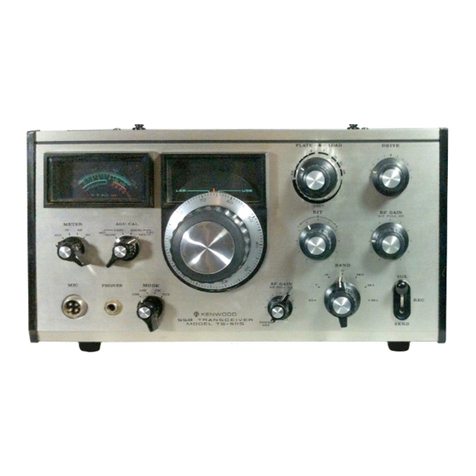
  9. Kenwood TS-60S User manual

Kenwood TS-60S User manual

I
5OMHz
ALL MODETRANSCEIVER
0
1994-1 PRINTEDINJAPAN
851-8252-00
(0)
1095
t-
Knob(Power) Microphone
(K29-4811-04) (T91-0528-051
SERVICE
MANUAL
Phone
jack
Panel
(Ell-0454-05) (A62-0296-03)
1
Knob(MHz) Knob
(UP)
(K29-4813-04) lK29-4815-041
Knob
(F.
LOCK) Knob(DOWN1
1
Knob
(K29-4812-04) lK29-4814-04) (K29-4817-04)
x
3
KnobIAFIRIT) Knob
(K29-4809-04)
x
2
(K29-4816-04)
x
6
1
Knob Knob(SOUIF SHIFT) Knob(MAIN) Knob
lK29-4817-04)
x
3
(K29-4810-04)
x
2
(K21-0793-041 (K29-4818-04)
x
2
CONTENTS
CIRCUITDESCRIPTION
...........................................
2
SEMICONDUCTORDATA
.....................................
21
DESCRIPTIONOFCOMPONENTS
.......................
25
PARTSLIST
............................................................
3.0
EXPLODEDVIEW
................................................
61
PACKING 64
ADJUSTMENT ....................................................... 65
TERMINAL FUNCTION
..........................................
83
CIRCUIT DIAGRAMS
I
PC BOARDVIEWS
LCD ASSY (838-0719-15)
..................................
86
FINALUNIT (X45-3490-00)
...............................
89
DIGITALUNIT (X46-318X-XX)
..........................
93
PLL UNlT 1x50-3200-00)
...................................
97
r
DDS (X58-4020-00)
............................................
99
VCO 1x58-4120-00)
..........................................
100
IFUNlT1x48-3110-00)
.....................................
104
ALC (X59-3990-00)
..........................................
104
TX-RX UNlT(X57-4570-00)
.............................
105
DSST (X59-4000-00)
........................................
109
SCHEMATIC DIAGRAM
.......................................
115
BLOCK DIAGRAM
............................................
117
MB-13(MOUNTINGBRACKET)
..........................
119
PG-2Y (DCCABLE)
............................................
119
MC-47 (MULTIFUNCTIONMICROPHONE)....... 120
SPECIFICATIONS
.................................................
121
CIRCUIT DESCRIPTION
FrequencyConfiguration
T
The TS-60s uses double conversion in all transmis-
sion modes, double conversion in all reception modes
except FM, and triple conversion in FM reception
mode. (Fg.1)
Table
1
Displayfrequency in each mode
Display
freq~
Transmit carrler frequency
...
MIX-2 73.04SMHz MIX-1 BM
0
MIC
AM
DET
MIX-1 73.045MHz MIX-2
RX
OUTPUT
Fig.
1
Frequencyconfiguration
1
The receiver frequency in SSB mode is given bythe
following equation when the receiver tone produced
by the input frequency (fl~)from the antenna is zero
beat (whenan SSB signal with a carrier point of
IN
is
zeroed in):
IN
=
ILOI
-
f~oz
-
CAR
Since all these frequencies are generated by the
PLL circuit, as shown in Figure 2 (PLL frequency con-
figuration), the receiver frequency is determined only
by the reference frequency,
~STD,
and the PLL divide
ratio. This means, the accuracy of the reference fre-
quency determines the accuracy of the operating fre-
quency of thetransceiver.
The accuracy ofthe referencecrystal oscillator used
in the TS-GOS is 10 ppm (-1 0 to +50°C). The accuracy
of theoptional temperature-compensatedcrystaloscil-
lator (TCXO, SO-2)is 0.5 ppm (-1 0 to +50°C).
In SSB transmission mode or in other modes, the
frequency is determined by the reference frequency
(~STD)
and the PLL divide ratio. Table 1 liststhedisplay
frequencies inthe various modes.
The pitchof the incomingsignal in CW modecan be
varied in 50-Hz steps inthe range 400 to 1000Hzwith-
out changing the center frequency of the
IF
filter (vari-
able CW pitch system).
FMtransmission iscarried out by applyingthe audio
signalfromthe microphonetothe 62.35-MHzVCOand
modulating f~oz.
2
PLL
CircuitConfiguration
The TS-60s PLL circuit uses a reference frequency
of 20MHz. and covers 40 to 6OMHz
(K),
50 to 54MHz
(E)
in 5- to 200-Hz steps, depending on how fast the
encoder is turned. Figure 2 shows the frequency con-
figuration of the PLLcircuit. Figure3 isa PLLblock dia-
gram.
1
1.
Referenceoscillatorcircuit
The referencefrequency
(~STD)
for frequency control
is generated by the 20-MHz crystal oscillator, XI and
Q12 (2SC2714(Y)). The reference frequencies for
other circuits are produced bydividing
~STD
bytwoand
byfive by IC2 (pPD74HC390G).
~STD
is divided bytwo
to produce a 10-MHz
PLL
reference signal, whichgoes
to lCll (CXD1225M)and lClOl (CXD1225M).
It
is in-
put tothe CAR oscillator section toproduce a 10.695-
MHz signal. The 4-MHz signal produced by dividing
fSTD by five goes to IC4 (SN16913P).
The crystal oscillator circuit can be replaced by an
optional TCXO (SO-2). The TS-60s can beswitchedto
the TCXO by removing a shorting jumper (WlN2).
1
r~
CIRCUIT DESCRIPTION
2.
LO2 (PLLloop)
The VCO of IC10 (KCH14) generates a signal of
62.35MHz. The 10-MHz reference frequency is ap-
plied to pin 5 of IC101 (CXD1225M), and is divided by
200 (800inFMmode)toproduce a50-kHz(12.5-kHz in
FM mode) comparison frequency. The output from
the VCO isappliedtopin 11 of IC101, and isdivided by
1247(4988in FMmode). Itisthen comparedwith the
50-kHz (12.5-kHz in FMmode) reference signal by the
phase comparator to lock the VCO frequency. Divide
ratio data is supplied bythe digital unit.
The output is amplified byamplifier Q18 (2SC2954)
and passes through a low-pass filter. The VCO is
modulated in FMmode.
c
3.
LO1 (PLL lwpl
Q1, 03(2SK508NV) in the X58-4120-00 are VCOs.
01generates a signal of 113.045to 123.044MHz; and
Q3, asignal of 123.045 to 133.045MHz.
K
type
Q3 (2SK508NV) in the X58-4120-00 are VCO. Q3
generates
a
signal of 123.045to 127.045MHz.
E
type
The 10-MHz reference signal is input to pin 5 of
lCl1 (CXD1225M) and is divided by 20 to produce
a
500-kHz comparison frequency. The output signal
from the VCO is mixed with a 75.045-to 75.545-MHz
signal from the PLL (described later)to producea38.0-
to 57.5-MHz signal. It is input to pin 11 of IC11, di-
vided, and compared with the 500-kHz signal by the
phase comparator, and the VCO frequency is locked.
Divide ratiodata is supplied bythe digital unit.
The 20-MHz reference signal is input to DDSl (X58-
4020-OO), and the output signal is mixed with a 4-MHz
signal byIC4togenerateasignal of 4.455
to4.955MHz
(in5-or 200-Hz steps). The signal ismixedwith the80-
MHz signal (4x 20-MHz reference frequency) by IC5
(SN16913P)to produce a 75.045 to 75.545MHz signal
(in 5-or 200-Hz steps).
4.
CAR
The 20-MHz reference signal is input to DDS2 (X58-
4020-OO), and the output signal is mixed by IC7 (SN
16913P)with the 10MHzsignal divided by IC2 to pro
duce a 10.695-MHzsignal. This signal passes through
the band-passfilter and amplifier and is outputfor local
oscillation and detection.
5.
DDS
The DDS is the same as that used inthe TS-50.
Fig.
2
PLL circuitfrequency configuration
CIRCUIT DESCRIPTION
Receiver CircuitConfiguration
The second IFsignal of 10.695MHz is split intotwo.
The configuration of the receiver circuit is double- One signal goes to the NB amplifier, and the other
conversion with a first IF of 73.045MHz and a second passes through the NB gate FET (3SK131). The signal
IF of 10.695
MHz.
and tripleconversion in FM mode then passes through the CF (XF2)and is detected by
IC2 (KCD04) in FM mode. In other modes, the signal
with
a
first
IF
Of
73.045MHz'
a
second
IF
Of
goes tothe IF filter of the X48-3110-00 unit. There are
10.695MHz, and athird IF of 455kHz. (Fig. 5)
The incoming signal from the antenna passes threetypes of IFfilter: 6-kHz. 2.7-kHz,and 500-Hz(500-
throughtheantenna switch relayonthefilter unit, then Hz is optional). The signal passing through the IF filter
goes to IC3 (KCD08), and is productdetected in SSB
through the ~O-MHzlow-pass filter. and goes to the
and
CW
modes,
and
envelope-detected
in
AM
mode,
TX-RX unit. The sianal oasses throuah a 20dB attenu-
-,
-
ator and 54-MHz low-pass filter in the TX-RX unit, and
goes through the band-pass filters. If AIP is off, the
signal passing through band-pass filter is amplified by
the RF amplifier, Q9. Q10and Q69 (2SK520x
3),
and is
input tothe first mixer, Q5to Q8(2SK520x 4). If AIP is
-
on, the signal bypasses Q9.010 and Q69and goes di-
rectlytothefirst mixer. Itis mixed with the LO1 signal
by the first mixer to produce a first IF signal of
73.045MHz.
The first IF signal of 73.045MHz passes through the
MCF (XFl),is amplified by Q17 (3SK131), and mixed
with the 62.35-MHz LO2 signal by the second mixer.
Q18 and Q19 (2SK520 x 2). to oroduce a second IF
1.
Receiverfront-end
The signal input to the TX-RX unit passes through
the switching circuit of the attenuator and the 60-MHz
low-pass filter, and goes to band-pass filters. If AIP is
off, D49and Dl1 turn on and D8and D9turn off, and
the signal passing through filter is amplified by about
10dB byQ9, Q10 and Q69 (2SK520x 3)and output to
the first mixer. If AIP is on, D49 and Dl
1
turn off and
D8and D9turn on, and the signal is output directly to
the first mixer without passing through 09, Q10 and
Q69. The first mixer, isa quad balanced mixer, Q5 to
08(2SK520 x
4).
(Fig.4)
signal of 10.695MHz.
TX-RX
UNIT
1x57-4570-00)
Fig.
4
Receiver front-end
TX-RX
UNIT
CIRCUIT DESCRIPTION
2.
Noise blanker circuits
The
10.695-MHz
IF signal generated from the first
IF of
73.045MHz
bythe second mixer is inputto IF am-
plifier
Q21 (3SK1311,
sent through
Q20,
amplified by
noise amplifier
0200. 0201,
and
0202 (2SC2714).
sent through buffer
Q203,
and noise-detected by
D200.
This signal switches
Q205. Q206,
and
Q209,
and controls
Q22
in the TX-RX unit.
Q22
controls
IF
amplifier
Q21
and blanks the noise.
7h
??7
TX-RX
UNlT
........................
PLL
UNlT
Fig.
6
Noise blanker circuits
7
CIRCUIT DESCRIPTION
3. SSB, AM, CW filter circuit
The second IF signal amplified
by
021is inputtothe
X48-3110-00 unit in all modes except FM.
If an optional CW filter (XF1) is installed and CW
NARROW is elected in CW mode, the signal passes
through XF1 according to the control signal from the
microcomauter. If XF1 is not installed or CW NAR-
XF2.
InAMmode,the signal passesthroughXF3 and XF2
,-
-
-.-
- ~~-
ROW is nbt selected, the signal passes through XF3
insertion loss
as in SSB mode if
AM
NARROW is selected. If AM
NARROW is not selected, the signal passes through
XF2 only.
In FM mode, the signal does not pass through the
filter circuit in this unit.
Item
Nominal center frequency
Centerfrequency deviation
Pass bandwdth and
Attenuation bandwidth
Rinnle
and XF2.
In SSB mode, the signal passes through XF3 and
-
~
CW
(OPTION)
m
Rating
'
10.695MHz
-
Withini20OHz at 6dB
22kHz or more at 6dB
i-l5kHz or less at 20dB
+2.4kHz or less at 60d~
?ri~w
Guaranteedattenuation
/
60dB or more with~nfo
i
4OkHz
Terminatingimpedance 12kRi5%16pFi5%
lNO--FOOuT
Bandwidth
XF1
:
500Hz
XF2
:
6kHz
XF3
:
24kHz
Table 4 MCF (L71-0249-05)
:
IF unit XF3
Fig. 7 Filter circuit
4. SSB, AM, CW detection circuit
After unwanted signal components have been re-
-
moved in the X4E3110-00 unit, the signal is input to
IC3IKCD08). The signalamplified by IC3 is mixedwith
the CAR signal input from CNll in SSB and CW
modes, and detected to output an audio signal. InAM
mode, the signal is envelope-detected
by
the diode
and capacitor to output an audio signal.
Item
5. FMdetection circuit
The impedance of the second IF signal amplified
by
021 is converted by 023 (RU201) in FM mode, and
unwanted signal components are removed by the CF
(XF2). The resulting signal is input to the detection IC
(IC2:KCD04). The signal is then mixedwiththe 10.24-
MHz oscillator signal to generate the 455-kHz signal.
The signal is passed through ceramic filter CFI, and
detected by the quadrature detector with the signal
phase-shifted by CD1
Rating
Nominalcenter frequency
1
10,695kHz
deviation
1
Within+80Hz at 6dB
.-.,..,..-....s
.,..v
,
.-"".-"?.
I
pears at the base of 031. When the
SQ~VR
is turned
Table 2 MCF (L71-0283-05)
:
IF unit XF1 (Option)
clockwise. the emitter voltaae of 031 increases and
6.
Squelch circuit
7
~ ~
~
~
~
~~
~~-
Insertion loss
1
Within 5dB
i
2dB
~~~~i~~ti~~
irnn~iianrr
1
19nnoifin~
p
Inall modes except FM, the 10.695-MHz IF signal is
detected
by
a diode in IC3, passed through 029 and
030, and a voltage proportional to the signal level ap-
-
Q32 is switchedon.
In FM mode, as the IF signal increases, the noise
level decreases, and the voltage at the SQ pin de-
creases, making the SC pin low. When the SO VR is
turned clockwise, the voltage at the SQ pin rises, and
the SC pin goes high. Current flows through R77, and
032turns on.
035 turns on to mutethe AF signal line. (Fig. 8)
Item
Rating
Table 3 MCF lL71-0433-05)
:
IF unit XF2
-
Nominalcenter frequency
Pass bandwidth
Atten~~atlonbandwidth
Ripple
Insenionloss
Guaranteedattenuation
Terminatingimpedance
'
10695MHz
GkHz or more
at
GdB
4OkHz
or
less at 60dB
2dB or less
3dB or less
60dB
or
more within fo
f
1MHz
12kn
+
10%
I~~F
+
10%
CIRCUIT DESCRIPTION
Fig.
8
Squelch circuit
7.
Signalstrength meter circuit
8.
AGC
circuit
In all modes except FM, the signalstrength meter The time constant for the signal envelope-detected
circuitcomprises operationalamplifier IC5. The signal, by IC3 is changed in each mode by the analog switch.
level-detected byIC3, is input to IC5
11/21
andamplified The effective value, not the peak value, is used in
AM
by about
8
dB by IC5 (212). mode. When
SLOW
is selected in
SSB
and CW
In FM mode, the level detection signal from IC2 is modes, the analog switch isturned on. (Fig.
9)
adjusted by VR2, selected by IC4 (BU4066BF)accord-
ing to the mode, andoutput directly tothe digital unit.
(Fig.
9)
CIRCUIT
DESCRIPTION
IC3 KCDOB
1
1
11
-
..
Y
+
LTI
SSB.
AM.
CW
IC2 KCDO4
-
FM
SM
FM
Fig.
9
S-meter
and
AGC
circuits
Transmitter CircuitConfiguration
The audio signal from the microphone enters CN15
of the TX-RX unit. The signal then goes to 038
(2SC3722K) of the microphone amplifier, and is split
and directed tothe SSB and FMsystems. In the SSB
system, the signal, itsgain properlyadjusted byVR7, is
amplified by
Q40
(2SC2712(Y)),balance-modulated
with the CAR signal (10695MHz)input from CN1l by
IC8 (KPC~O~~HA),passed through 042 (2SC2712(Y)).
and sent to the ciystal filter in the X48-3110-00 unit.
The SSB signal passing through the filter is amplified
by Q43 (3SK131M).
The62.35-MHz LO2signal fromthe PLL unit is input
from CN3 of the TX-RX unit, and mixed with the
10.695-MHz signal amplified by Q43. 046, and 047
(3SK131(M))toproduce
a
73.045-MHz signal. The LO1
signalfromthe PLL unit isinputfrom CN2 of theTX-RX
unit, and mixed with the 73.045-MHz signal by 048
and 049 (3SK184(R))to generate the desired signal.
The signal passes through the band-pass filter and is
amplified by 050(2SC2954) to produce the drive out-
put, which goes tothe final unit from CN19.
The signal is amplified to the appropriate power
level for the type by the final unit. Harmonic compo-
nents are attenuated by the filter unit, and the signal is
output from the antenna connector.
In FM mode, the audio signal amplified by micro-
phone amplifier Q38 and Q39 is input to CN1 of the
PLL unit, and passes through the pre-emphasis and
IDC circuit ofIC201 to modulate LO2 (6235MHr).
InAMmode, the signal is generated by unbalancing
the carrier of SSB balance modulator IC8.
In CW mode, Q59 of the TX-RX unit isswitched by
the key, and the signal is input to IC1 of the digital unit.
The sidetone monitorsignal is generated by X59-4000-
00 inthe TX-RX unit, and output fromthe speaker. The
CWcontrol signal is output from IC1 of the digital unit,
and input from CN17 of the TX-RX unit to switch 046
and 047and generate the CW signal. (Fig. 10)
I
CIRCUIT DESCRIPTION
Fig.
10
Transmitter section block diagram
CIRCUIT DESCRIPTION
1.
ALC
circuit
The forward wave voltage detected inthe filter unit
passes through CN18 inthe TX-RX unit, its level is ad-
justed by VR14, and
it
is applied to the differential
amplifier comprising Q1 and Q2 (2SC2712(Y)
x
2) in
IC11. When VSF is applied to the base of Q1, the
emittervoltage of 01and Q2 increases andthe current
flowing through the base of 02decreases; thus the
collector voltage rises. Whenthis voltageexceeds the
emitter voltage of Q3 (2SC2712iY))(about 1.8V) plus
VBE
(about0.6V),the current flows through the base
of 03and the collector voltage drops. ALC time con-
stants
C
and
R
are connected tothis collector.
The collector voltage change is shifted by Q4
(2SK208)and D2(3.6V),and matchedwith the voltage
for keying by
05
and D3 (RLS73)to generate the ALC
voltage. This ALC voltage activates ALC by lowering
the secondgate voltage of Q43(3SK131(M))of theTX-
RX unit. (Fig. 11)
2.
Power control circuit
Power is controlled by lowering the base voltage of
02in IC11. As the base voltage of Q2 decreases, the
emitter voltage of 01 and Q2 decreases. This acti-
vates ALC and reduces the power even if the base
voltage (VSF)of 01is low. The power is changed by
IC12. In
AM
mode. 063 turns on, and the power is
reduced to about 114 of the power in other modes.
(Fig. 11)
VS
R
VSF
Fig.
11
ALC
and
power control circuits
CIRCUIT DESCRIPTION
3.
Protectioncircuit
Whenthe reflectedwave voltage (VSR)detected by
thefilter unit rises, Q6(2SC2714(Y))in IC11turns on to
reducethe voltage of the ALC time constant line. The
drive is decreased and the power is reducedtoprotect
the final transistor.
4.
Temperature protection
If the final heat sink temperature rises, 08in the
final unit turns on and the fan starts running at low
speed in both transmit and receive modes. If the final
heat sink temperature rises further, Q9turns on, and
the fan rotates at mediumspeed in both transmit and
receive modes. If the temperature rises further still,
the fan rotates at high speed in transmit mode, and at
7
medium speed in receive mode to reduce the fan
noise.
If the temperature continues to rise, the tempera-
ture detection port of the microcomputer (IC1 in the
digital unit) is made high to reduce the RF output forci-
bly. If the fan fails or does not rotate because some-
thing is stopping it, the RF output is forcibly reduced in
the same way.
2.
Reset circuit
IC4 (M62003FP)monitors Vcc applied to the micro-
computer. If the voltage falls below2.15V, the IC out-
putsa reset signal (low)tothe microcomputer, andthe
CPU initializes all internal data (includingmemorychan-
nel data). The reset signal is not output when the
power isturnedon or off or 14V isturned on or off. Itis
output when the battery voltage level goes low and
14V is turned on or off.
C35 generates the signal width (td)requiredtoreset
the microcomputer. (Fig.12)
DigitalControl Circuit
4.35~
The TS-GOS digital control circuit comprises a 16-bit
2,15V
microcomputer (M37702M4A-FP), a reset IC
(M62003FP), an EEPROM (NM93C66LEM8 or
AT93C66-10S12.7), a latch (TC74HC573AFL and a de-
coder (TC74HC238AF). The latch and decoder are
1
'
1
usedtoexpandtheoutput ports. The decoderoutputs
an enable signal pulse.
-
1.
Power button
With this transceive, the power is turned on and off
RESET
RESET
by the microcomputer. When the power bunon is
pressed, the microcomputer detects it and energizes,
Fig.
12
Reset circuit
the power relay to supply 14V to the transceiver.
When the power button is pressed to turn the trans-
ceiver off, the microcomputer checks it a little longer
than when turning the power on, and deenergizes the
power relay.
Fig.
13
Digital control block diagram
-
CIRCUIT DESCRIPTION
Y~
3.
Backupcircuit
This transceiver has two kinds of data stored in the
microcomputer and EEPROM. User data, such as
memory channeldata, isstored in the microcomputer,
andadjustment data, such as metercurves, isstored in
the EEPROM. The EEPROMdata is retainedwhen the
power supply voltage is off, but power is required to
retain the microcomputer data. If 14V is not cut off.
powerissuppliedfromthe 5VAVR inthe digital unit. If
14Viscutoff, powerissuppliedfrom alithiumbattery.
To retain data with the lithium battery, the microcom-
puter must be in backup mode. So, the backup circuit
shown in Figure.14detects a voltage drop in the 14V
line and outputs a backup request signal to the micro-
computer.
,--
4.
PLL
and
DDS
control circuit
The TS-60s has three PLLs and two DDSs The
main microcomputer outputs frequency data to the
PLLs and DDSs serially according to the display fre-
quency.
5.
TX-RX unit control signal circuit
The microcomputer sends the mode signal, IF filter
select signal, and power signal to the TX-RX unit.
It
receives meter signals and standby switch signals
from the TX-RX unit, displays data on the meters, and
performs the transmit operation. The output signal
from the microcomputer goes to the serial-to-parallel
converter (TC9174F).(Fig. 15)
Fig.
14
Backup circuit
Fllfer
s~gnal
6XHz
Filtersmgnal
Z.4kHz
Filterltynal
0
5kHz
ABKalgnsl
Powerolgnal 'LOW.
Powerr8ynal'MID'
Powsreignal 'HI'
Pawaragnal'MID'
powsr alynal
'LOW'
CWmods
signal
SSB
madaslgnal
AM
modenlgnal
FM
mode
agnal
AF
An
.,gna1
M37702M4A
MONITOR s~gnal
RX
BLANKING
s8gn.l
DIGITAL
UNiT
TX-RX
UNIT
Fig.
15
TX-RX unit controlsignal circuit
CIRCUIT DESCRIPTION
6.
Switch
AID
input
7.
EEPROM
The voltage divided by nineswitches
S16, 52
to
S9,
Adjustment data is stored in the EEPROM, which
S10
to
S15,
and
S17
to
S19
is applied tothe PJD input consistsof
256
16-bit registers. Datacan bewritten to
pin of the microcomputer when a button is pressed. and read from the EEPROM. Each time the power is
(Fig.
16)
When twoor more buttonsinthe same group switchedon, data is read fromthe EEPROM. If corrupt
are pressed at the same time, only the buttonwith the data is detected, the default adjustment data is used.
highest priority is detected (listedbelow). Adiustment data can be written into the EEPROM in
KADl
I
KADZ
1
Priority
s16
1
SPLIT
1
SIT
IF.LOCK
I
1
S3
/
AIPIAT
I
S12
I
DOWN
1
2
S5
S6
S7
Table
5
S8
I
M>V
I
S17
I
A=B
service adjustment mode. (Fig.
17)
-
RIT
M
IN
SCAN
7
-
Fig.
17
EEPROMcircuit
S9
I
CLR
I
S18
I
SSBICW
1
8
S2
I
MENU
1
S19
I
FMIAM
1
9
N
ul
-
'2
'0
DIGITAL
UNIT
I
I
LCD
ASSY
..
S14
S15
S10
Flg.
16
Switch
AID
input circuit
MHz
AiB
MN
4
5
6
r
CIRCUIT DESCRIPTION
/
8.
Encoder circuit
The encoder is a mechanical one. The waveforms frequency step is made coarse toensure smooth tun-
of the encoder pulses are rectified by IC3 and IC4 ing and frequency change. The minimum frequency
(TC4S584F)in the LCD assembly, and the number of step is
5
Hz
(50
Hz
in
FM
mode);the maximum. 200
Hz
pulses is counted by the hardware counter in the mi-
(2kHz
in FM mode). The frequency step is changed
crocomputer. The rotational speed of the encoder is continuously according to the speed of rotation. (Fig.
detected. When the encoder isturned slowly, the fre- 18)
quency stepis madefine; whenitisturned quickly, the
5V 5v
M37702M4A
ENCODER
DIGITALUNIT
!
!
LCDASSY
I
Fig.
18
Encoder circuit
9. Busy signal 11. Beep
The level of the port is monitored in receive mode, The beep signal is generated using the timer in the
and busy indication and busy stop are performed dur- microcomputer. The menu enable data (beeponloff.
ing scanning. mode beep, warning Morse) is recognized, and the
necessary code is output.
A
dot lasts about 40ms; a
10.
Dimmer control
dash, about 120ms. The oscillation frequency is about
The dimmer is controlled in five steps (including 1.4kHz.
r
OFF). The lamp isturned on oroff bypin
7
of IC2of the
switch unit. The brightness of the dimmer lamp is
determined by pins 5 and
6
of IC2. (Fig. 19)
Fig. 19 Dimmer control circuit
CIRCUIT DESCRIPTION
12.
Subtone
The subtone frequency is converted from digital to
analog
by
a
ladder resistor, and a pseudo-sine wave,
including the
1750-Hz
tone, is output. (Fig.
20)
Fig.
20
Subtone
circuit
CIRCUIT DESCRIPTION
13.
Settings
Contents of menu
If you holddown the
F.
LOCK
key for more than
1.5
seconds,
a
menu is displayed. You can change the
menu number with the encoder, change between
menus
A
and
B
with the
A/B
key, and change settings
with the UPIDOWN key.
pttchchange
3
tone onlof.
le Morse on,
ning Morse
8
change
w~tch~ng
:
150-Hz
stec
now
orotect
2
(overwrite?/eraseinhib
when
1-MH:
..,,,,-a
z
step is on
, , , ~,
72
I
USB
transmiVrece~vecarrier point setting
/
-100-200
r-off onloif
funct~on
I
manual.
CIRCUIT DESCRIPTION
PF
key
functions
Three kinds of function (panel function, menu
NB
function, and non-panel function) are assigned to the
four PF keys on the microphone. To assign
a
function
to a key, specify the number in the following table us-
ing the UPIDOWN key in the order of
67
to
70
(PFI to
PF4) in menu
B
mode. The PF keys are named PF1,
PF2, PF3, and PF4 from the left, as viewed from the
front of the microphone.
Menu
16
Menu
17
-
An
-
NB
-
F.
LOCK
-
vlenu 52
vlenu 53
vlenu 54
.
..
DOWN
MHz
TF-SET
A=B
vlenu
66
IFF
14.
VCO
switching data
Frequency
VCO
data
40MHz
<
f
<
5OMHz
5OMHz
<
f
<
6OMHz

Other manuals for TS-60S

3

Other Kenwood Transceiver manuals

Kenwood TM-V708A User manual

Kenwood

Kenwood TM-V708A User manual

Kenwood NEXEDGE NX-800 series User manual

Kenwood

Kenwood NEXEDGE NX-800 series User manual

Kenwood NEXEDGE NX-800H User manual

Kenwood

Kenwood NEXEDGE NX-800H User manual

Kenwood TM-D700A User manual

Kenwood

Kenwood TM-D700A User manual

Kenwood TK-3212 User manual

Kenwood

Kenwood TK-3212 User manual

Kenwood TS-590SG Manual

Kenwood

Kenwood TS-590SG Manual

Kenwood TS-930S User manual

Kenwood

Kenwood TS-930S User manual

Kenwood TS-590S User manual

Kenwood

Kenwood TS-590S User manual

Kenwood TS-590SG Manual

Kenwood

Kenwood TS-590SG Manual

Kenwood TK-280 User manual

Kenwood

Kenwood TK-280 User manual

Kenwood TK-8102 User manual

Kenwood

Kenwood TK-8102 User manual

Kenwood TR-7400A User manual

Kenwood

Kenwood TR-7400A User manual

Kenwood TK-280 User manual

Kenwood

Kenwood TK-280 User manual

Kenwood TK-380 User manual

Kenwood

Kenwood TK-380 User manual

Kenwood TS-850S User manual

Kenwood

Kenwood TS-850S User manual

Kenwood TH-K40A User manual

Kenwood

Kenwood TH-K40A User manual

Kenwood TR-9130 User manual

Kenwood

Kenwood TR-9130 User manual

Kenwood TM-261A User manual

Kenwood

Kenwood TM-261A User manual

Kenwood TK-2407 User manual

Kenwood

Kenwood TK-2407 User manual

Kenwood TM-D700A User manual

Kenwood

Kenwood TM-D700A User manual

Kenwood NX-3000 series User manual

Kenwood

Kenwood NX-3000 series User manual

Kenwood TK-868HG User manual

Kenwood

Kenwood TK-868HG User manual

Kenwood TM-D710GA User manual

Kenwood

Kenwood TM-D710GA User manual

Kenwood PKT-23 User manual

Kenwood

Kenwood PKT-23 User manual

Popular Transceiver manuals by other brands

Aurora VLX-TC1-C Product guide

Aurora

Aurora VLX-TC1-C Product guide

Yaesu FT-950 manual

Yaesu

Yaesu FT-950 manual

Alinco DJ-CRX7 instruction manual

Alinco

Alinco DJ-CRX7 instruction manual

Midland 13-513 Service manual

Midland

Midland 13-513 Service manual

Alinco DJ-G29T instructions

Alinco

Alinco DJ-G29T instructions

Nokia NSB-1 Series Troubleshooting instructions

Nokia

Nokia NSB-1 Series Troubleshooting instructions

Intek DRS-5070 owner's manual

Intek

Intek DRS-5070 owner's manual

Nokia NME-2A Series Troubleshooting instructions

Nokia

Nokia NME-2A Series Troubleshooting instructions

Yaesu FT-100D operating manual

Yaesu

Yaesu FT-100D operating manual

Midland G18 Instruction guide

Midland

Midland G18 Instruction guide

Midland M24-S quick guide

Midland

Midland M24-S quick guide

Icom IC-A110 Service manual

Icom

Icom IC-A110 Service manual

Standard Horizon PHANTOM PS1000 owner's manual

Standard Horizon

Standard Horizon PHANTOM PS1000 owner's manual

Icom IC-G88-T instructions

Icom

Icom IC-G88-T instructions

Icom IC-2A Maintenance manual

Icom

Icom IC-2A Maintenance manual

Alinco DR-M06T Adjustment points

Alinco

Alinco DR-M06T Adjustment points

Radio Shack HTX-245 Service manual

Radio Shack

Radio Shack HTX-245 Service manual

Robyn T-240D user manual

Robyn

Robyn T-240D user manual

manuals.online logo
manuals.online logoBrands
  • About & Mission
  • Contact us
  • Privacy Policy
  • Terms and Conditions

Copyright 2025 Manuals.Online. All Rights Reserved.