logo
Brands
  1. Home
  2. •
  3. Brands
  4. •
  5. Laird
  6. •
  7. Motherboard
  8. •
  9. Laird Lyra P User manual

Laird Lyra P User manual

This manual suits for next models

1

Other Laird Motherboard manuals

Laird 453-00062-K1 Installation and operating instructions

Laird

Laird 453-00062-K1 Installation and operating instructions

Laird Lyra S User manual

Laird

Laird Lyra S User manual

Laird RM126 Series User manual

Laird

Laird RM126 Series User manual

Popular Motherboard manuals by other brands

DFI SD170 user manual

DFI

DFI SD170 user manual

ASROCK ROMED8-2T user manual

ASROCK

ASROCK ROMED8-2T user manual

Asus P2L97A user manual

Asus

Asus P2L97A user manual

Winmate IC70 user manual

Winmate

Winmate IC70 user manual

Asus MES-B user manual

Asus

Asus MES-B user manual

Grantech SYS8F377VGGA-3OMN user manual

Grantech

Grantech SYS8F377VGGA-3OMN user manual

Telit Wireless Solutions SL869-3DR user guide

Telit Wireless Solutions

Telit Wireless Solutions SL869-3DR user guide

Texas Instruments ADS8372EVM user guide

Texas Instruments

Texas Instruments ADS8372EVM user guide

Commell MS-C73 user manual

Commell

Commell MS-C73 user manual

Gigabyte GA-9IVDT user manual

Gigabyte

Gigabyte GA-9IVDT user manual

IBT Technologies MB860 user manual

IBT Technologies

IBT Technologies MB860 user manual

Nvidia TEGRA DG-04927-001_V01 user guide

Nvidia

Nvidia TEGRA DG-04927-001_V01 user guide

Intel D33217CK specification

Intel

Intel D33217CK specification

Asus F1A55-M LX PLUS R2.0 user manual

Asus

Asus F1A55-M LX PLUS R2.0 user manual

EPC EPC9147C quick start guide

EPC

EPC EPC9147C quick start guide

Asus EX-B760M-V5 D4 quick start guide

Asus

Asus EX-B760M-V5 D4 quick start guide

EPOX MU-8KHA0010 user manual

EPOX

EPOX MU-8KHA0010 user manual

Ski-Doo Bombardier MPEM 219 700 090 user guide

Ski-Doo

Ski-Doo Bombardier MPEM 219 700 090 user guide

https://manuals.online logo
https://manuals.online logoBrands
  • About & Mission
  • Contact us
  • Privacy Policy
  • Terms and Conditions

Copyright 2026 Manuals.Online. All Rights Reserved.

A
Version 1.3
https://www.lairdconnect.com/
2
© Copyright 2022 Laird Connectivity
All Rights Reserved
Americas: +1-800-492-2320
Europe: +44-1628-858-940
Hong Kong: +852-2762-4823
Version
Date
Notes
Contributors
Approver
1.0
27 April 2022
First Release
Raj Khatri
Dave Drogowski
Jonathan Kaye
1.1
10 June 2022
Corrected Figure 4 in 8.4 Push Button
and LED
Florian Baumgartl
Raj Khatri
Dave Drogowski
Jonathan Kaye
1.2
19 Aug 2022
Added note about silkscreen labelling
on board revisions 2.2 and previous
for SW1 in 6 Software Development
Selection Switch SW1
Dave Drogowski
Jonathan Kaye
1.3
31 Aug 2022
Added section 8.4.1 BOOT pin (PC07)
and BUTTON 0 (silkscreen BTN0)
Raj Khatri
Dave Drogowski
Jonathan Kaye
https://www.lairdconnect.com/
3
© Copyright 2022 Laird Connectivity
All Rights Reserved
Americas: +1-800-492-2320
Europe: +44-1628-858-940
Hong Kong: +852-2762-4823
1Overview......................................................................................................................................................................4
2Laird Connectivity Lyra P Part Numbers........................................................................................................................4
3Kit Contents.................................................................................................................................................................5
4Main Board –Features.................................................................................................................................................5
4.1 Key Features.......................................................................................................................................................5
5Understanding the Development Board.........................................................................................................................6
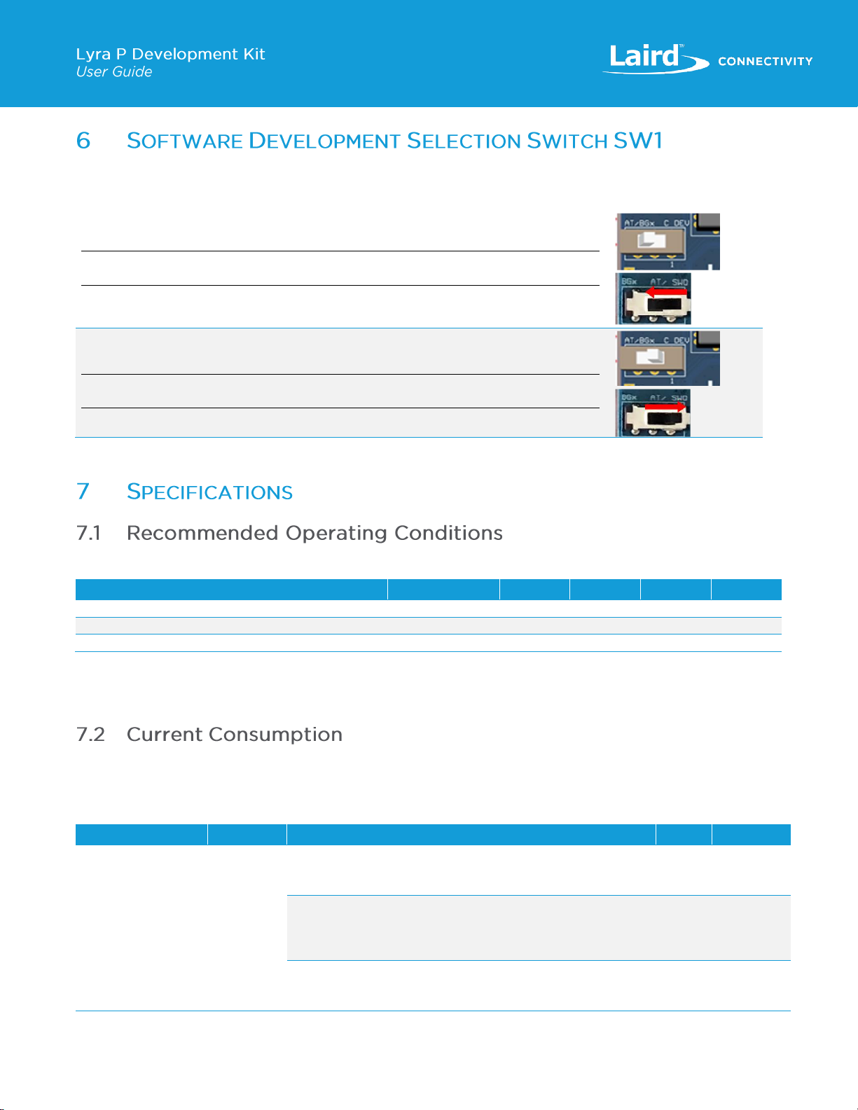
6Software Development Selection Switch SW1...............................................................................................................7
7Specifications...............................................................................................................................................................7
7.1 Recommended Operating Conditions...................................................................................................................7
7.2 Current Consumption...........................................................................................................................................7
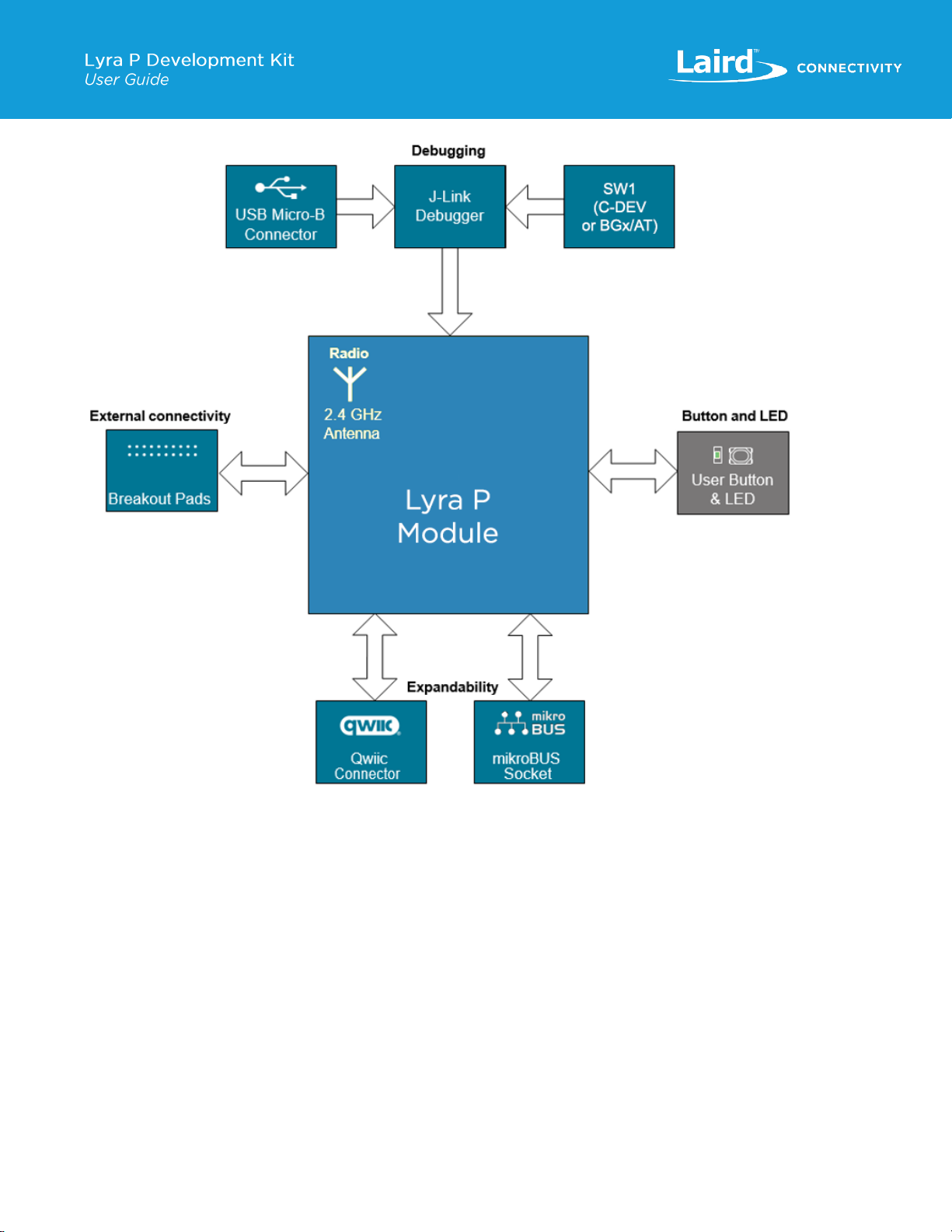
8Functional Blocks.........................................................................................................................................................8
8.1 Hardware Block Diagram.....................................................................................................................................8
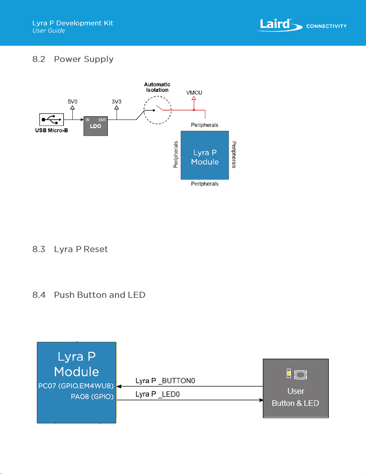
8.2 Power Supply....................................................................................................................................................10
8.3 Lyra P Reset .....................................................................................................................................................10
8.4 Push Button and LED........................................................................................................................................10
8.4.1 BOOT pin (PC07) and BUTTON 0 (silkscreen BTN0)....................................................................................11
8.5 On-board Debugger...........................................................................................................................................11
8.6 Hardware Connectors........................................................................................................................................12
8.6.1 Breakout Pads Pinout...................................................................................................................................13
8.6.2 MikroBUS Socket.........................................................................................................................................14
8.6.3 Qwiic Connector...........................................................................................................................................15
8.6.4 Debug USB Micro-B Connector ....................................................................................................................15
9Debugging.................................................................................................................................................................16
9.1 On-board Debugger...........................................................................................................................................16
9.2 Virtual COM Port...............................................................................................................................................16
10 Schematic, Assembly Drawing, 3DModel....................................................................................................................16
https://www.lairdconnect.com/
4
© Copyright 2022 Laird Connectivity
All Rights Reserved
Americas: +1-800-492-2320
Europe: +44-1628-858-940
Hong Kong: +852-2762-4823
The Lyra P Development Kit is an ultra-low cost, small form factor development and evaluation platform for the Lyra P
Wireless Bluetooth® Module.
The Lyra P Development Kit is focused on rapid prototyping and concept creation of IoT applications. It is designed around the
Lyra P Module, based on the EFR32BG22 System-on-Chip, which is an ideal device family for developing energy-friendly
connected IoT applications.
The kit features a USB interface, an on-board SEGGER J-Link debugger, one user-LED and button, and support for hardware
add-on boards via a mikroBus socket and a Qwiic connector. The hardware add-on support allows developers to create and
prototype applications using a virtually endless combination of off-the-shelf boards from mikroE, sparkfun, AdaFruit, and
Seeed Studios.
Module
▪Lyra P Wireless Bluetooth® Module
▪High performance 2.4 GHz radio
▪32-bit ARM® Cortex®-M33 with 76.8 MHz maximum operating frequency
▪512 kB flash and 32 kB RAM
Features
▪User LED and push button
▪20-pin 2.54 mm breakout pads
▪mikroBUS™ socket
▪Qwiic® connector
▪SEGGER J-Link on-board debugger
▪Virtual COM port
▪Packet Trace Interface (PTI)
▪USB-powered.
▪Software Development Selection Switch SW1 to select between 2 options (AT/BGx or C-DEV) –
SEE NOTE BELOW.
Note: Versions of the development board silkscreen prior to v2.3 may list SW1 as BGx or
AT/SWO. On these boards, BGx should be understood to be AT/BGx and AT/SWO
should be understood to be C-DEV. See 6 Software Development Selection Switch
SW1
Software
▪AT Command Set - Fully featured and extensible, proven over 5+ years. Simplest
implementation with all key Wireless Xpress features, proven over 5 years
▪Wireless Xpress - Frozen at current release, path for existing Silicon Labs customers. Secure
FOTA-capable firmware, Xpress command API for iOS/Android
▪C Code - Full software development with Silicon Labs SDK and toolchain. Use Simplicity Studio
IDE for full functionality of Silicon Labs HW/SW
Part Number
Description
453-00090-K1
Lyra Series - Development Kit - Bluetooth v5.3 PCB Module with integrated antenna
Applicable to following Lyra P part numbers:
Part Number
Product Description
453-00090R
Lyra Series - Bluetooth v5.3 PCB Module with integrated antenna - Tape / Reel
453-00090C
Lyra Series - Bluetooth v5.3 PCB Module with integrated antenna –Cut / Tape
https://www.lairdconnect.com/
5
© Copyright 2022 Laird Connectivity
All Rights Reserved
Americas: +1-800-492-2320
Europe: +44-1628-858-940
Hong Kong: +852-2762-4823
All kits contain the following items:
Development Board
Contains soldered Lyra P module and exposes all available hardware interfaces.
Power Options
USB cable (x1) –Type A to micro type B. Also provides serial via onboard USB –UART chip
The Lyra P Development Kit has been designed to simplify IoT development with the Lyra P wireless module. The kit includes
a mikroBUS™ socket and Qwiic® connector, allowing users to add features to the kit with a large selection of off-the-shelf
boards.
Programming the Lyra P Development Kit is easily done using a USB Micro-B cable and the on-board J-Link debugger. A USB
virtual COM port provides a serial connection to the target application, and the Packet Trace Interface (PTI) offers invaluable
debug information about transmitted and received packets in wireless links. The Lyra P Development Kit is supported in
Silicon Labs’ Simplicity Studio™ and a Board Support Package (BSP) is provided to give application developers a flying start.
Connecting external hardware to the Lyra P Development Kit can be done using the 20 breakout pads which present
peripherals from the Lyra P such as I2C, SPI, UART and GPIOs. The mikroBUS socket allows inserting mikroBUS add-on
boards which interface with the Lyra P through SPI, UART or I2C. The Qwiic connector can be used to connect hardware from
the Qwiic Connect System through I2C.
The following key hardware elements are included on the Lyra P Development Kit:
▪Lyra P Wireless Module with 76.8 MHz operating frequency, 2.4 GHz ceramic antenna for wireless transmission, 512 kB
kB flash, and 32 kB RAM
▪One LED and one push button
▪On-board SEGGER J-Link debugger for easy programming and debugging, which includes a USB virtual COM port
and Packet Trace Interface (PTI)
▪MikroBUS™ socket for connecting click boards™ and other mikroBUS add-on boards
▪Qwiic® connector for connecting Qwiic Connect System hardware
▪Breakout pads for GPIO access and connection to external hardware
▪Reset button
▪Software Development Selection Switch SW1 to select between 2 options (AT/BGx or C-DEV) –SEE NOTE BELOW.
Note: Versions of the development board silkscreen prior to v2.3 may list SW1 as BGx or AT/SWO. On these
boards, BGx should be understood to be AT/BGx and AT/SWO should be understood to be C-DEV. See 6
Software Development Selection Switch SW1
https://www.lairdconnect.com/
6
© Copyright 2022 Laird Connectivity
All Rights Reserved
Americas: +1-800-492-2320
Europe: +44-1628-858-940
Hong Kong: +852-2762-4823
Note: Versions of the
development board silkscreen
prior to v2.3 may list SW1 as BGx
or AT/SWO. On these boards,
BGx should be understood to be
AT/BGx and AT/SWO should be
understood to be C-DEV. See 6
Software Development Selection
Switch SW1
Figure 1: Lyra P development board layout
https://www.lairdconnect.com/
7
© Copyright 2022 Laird Connectivity
All Rights Reserved
Americas: +1-800-492-2320
Europe: +44-1628-858-940
Hong Kong: +852-2762-4823
Development board switch SW1 is used for selecting between two Software Development types, namely Bluetooth Xpress /
AT Commands or C Code Development, as described below. SW1 is used to determine the behaviour of the Development
board. Two possible switch positions are available as follows:
AT/BGx (Left-hand position) - This position should be used when Silabs’ Bluetooth
Xpress or Laird Connectivity’s Lyra AT-Interface application is being evaluated.
Note: On development boards 2.2 and prior, AT/BGx is labelled BGx.
C-DEV (Right-hand Position) –This position should be used when native C code
development, using the samples provided by Silabs Simplicity Studio is being performed.
Note: On development boards 2.2 and prior, C-DEV is labelled AT/SWO.
The default position for SW1 is the right-hand position, ‘C-DEV’(previously labeled AT/SWO).
Table 1: Recommended operating conditions
Parameter
Symbol
Min
Typ
Max
Unit
USB Supply Input Voltage
VUSB
-
+5.0
-
V
Supply Input Voltage (VMCU supplied externally)
VVMCU
+3.31
V
Operating Temperature
TOP
-
+20
-
˚C
1 The typical supply voltage to the Lyra P is 3.0 V, but the maximum voltage is a function of temperature and average lifetime
current load. Over a 10-year lifespan, the average lifetime current load should not exceed 60 mA when the supply voltage is
3.3 V. See the Lyra P datasheet for more information.
The operating current of the board greatly depends on the application and the amount of external hardware connected. See
Table 2 for typical current consumptions for the Lyra P and the on-board debugger. Note that the numbers are taken from the
data sheets for the devices. For a full overview, see the Lyra P datasheet.
Table 2: Current consumption
Parameter
Symbol
Condition
Typ
Unit
Lyra P Current
Consumption1
IBGM
MCU current consumption in EM0 mode with all peripherals
disabled (module supply voltage = 3.0 V, VSCALE2, 38.4
MHz crystal, CPU running Prime from flash at 25 ˚C)
28
µA/MHz
Radio system current consumption in receive mode, active
packet reception (VDD = 3.0 V, MCU in EM1 and all MCU
peripherals disabled, HCLK = 38.4 MHz, 1Mbit/s, 2GFSK, f =
2.4 GHz at 25 ˚C)
3.8
mA
Radio system current consumption in transmit mode (VDD
= 3.0 V, MCU in EM1 and all MCU peripherals disabled,
HCLK = 38.4 MHz, f = 2.4 GHz, CW, 6 dBm output powerat
8.4
mA
https://www.lairdconnect.com/
8
© Copyright 2022 Laird Connectivity
All Rights Reserved
Americas: +1-800-492-2320
Europe: +44-1628-858-940
Hong Kong: +852-2762-4823
Parameter
Symbol
Condition
Typ
Unit
25 ˚C)
On-board Debugger
Sleep Current
Consumption2
IDBG
On-board debugger current consumption when USB cableis
not inserted (EFM32GG12 EM4S mode current consumption)
80
nA
1 From Lyra P data sheet
2 From EFM32GG12 data sheet
The core of the Lyra P Development Kit is the Lyra P Bluetooth® Module. Refer to Understanding the Development Board for
placement and layout of the hardware components.
An overview of the Lyra P Development Kit is illustrated in the figure below.
https://www.lairdconnect.com/
9
© Copyright 2022 Laird Connectivity
All Rights Reserved
Americas: +1-800-492-2320
Europe: +44-1628-858-940
Hong Kong: +852-2762-4823
Figure 2: Lyra P DVK block diagram
https://www.lairdconnect.com/
10
© Copyright 2022 Laird Connectivity
All Rights Reserved
Americas: +1-800-492-2320
Europe: +44-1628-858-940
Hong Kong: +852-2762-4823
The kit is powered by the debug USB cable as illustrated in the figure below.
Figure 3: Lyra P DVK power diagram
The 5 volt power net on the USB bus is regulated down to 3.3 V using an LDO (low-dropout regulator). An automatic isolation
circuit isolates the LDO when the USB cable is not plugged in.
Power can be injected externally on the VMCU net if the USB cable is removed, and no other power sources are present on
the kit. Failure to follow this guideline can cause power conflicts and damage the LDO.
The Lyra P can be reset by a few different sources:
▪A user pressing the RESET button.
▪The on-board debugger pulling the #RESET pin low.
The kit has one user push button marked BTN0 and one LED marked LED0 that are each connected to a GPIO on the Lyra
P. The button is connected to pin PC07 and it is debounced by an RC filter with a time constant of 1 ms. The logic state of the
button is high while the button is not being pressed, and low when the button is pressed. The LED is configurable in firmware
for user’s application. See BOOT pin (PC07) and BUTTON 0 (silkscreen BTN0) usage information.
Figure 4: Lyra P DVK Button and LED