QUICK START GUIDE
EPC – EFFICIENT POWER CONVERSION CORPORATION | WWW.EPC-CO.COM | COPYRIGHT 2017 | | 3
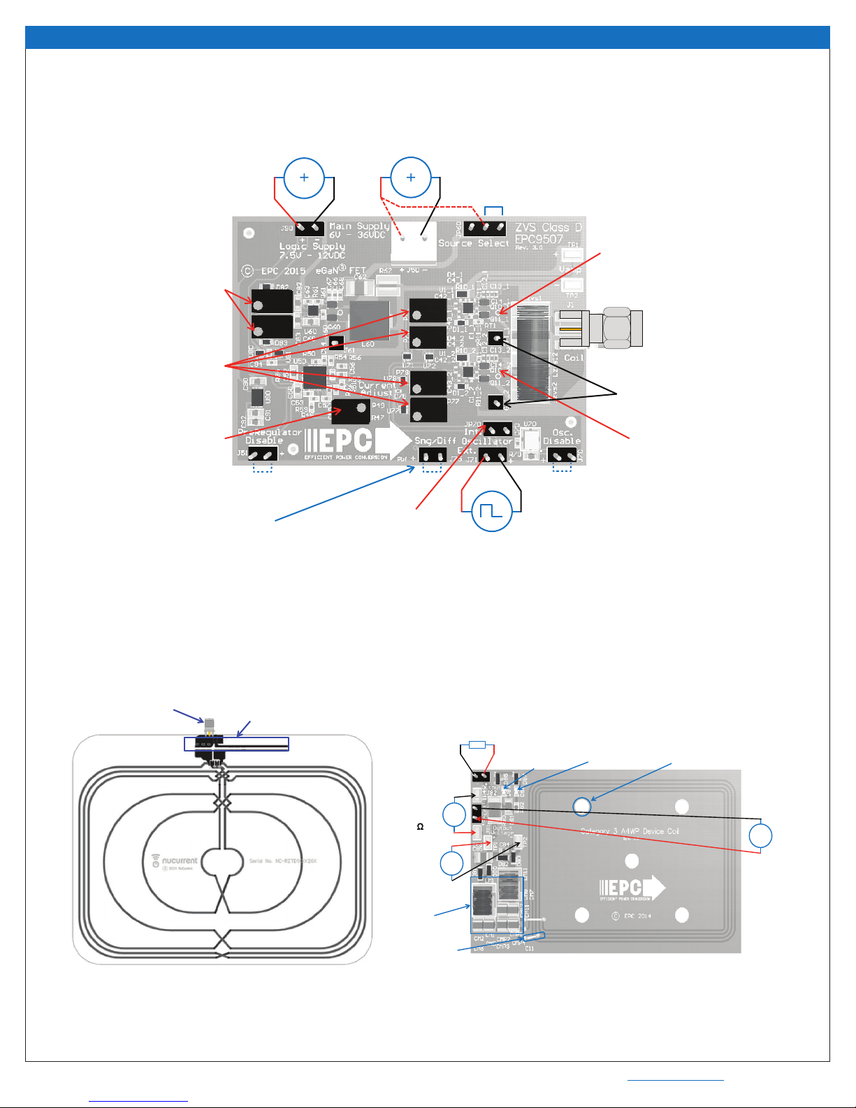
Demonstration System EPC9112
MECHANICAL ASSEMBLY
The assembly of the EPC9112 Wireless Demonstration kit is simple and
shown in Figure 1.The source coil and amplier have been equipped with
reverse polarity SMA connectors. The source coil is simply connected to
the amplier.
The device board does not need to be mechanically attached to the
source coil.
DESCRIPTION
The Amplier Board (EPC9507)
Figure 1 shows a diagram of the EPC9507 ZVS class-D amplier with pre-
regulator. The pre-regulator is set to a specied DC current limit (up to 1.5
A) by adjusting P49 and operates from 8 V through 36 V input. The output
voltage of the pre-regulator is limited to approximately 2 V below the
input voltage. The pre-regulator can be bypassed by moving the jumper
(JP60) over from the right 2 pins to the left 2 pins. To measure the current
the amplier is drawing, an ammeter can be inserted in place of the jumper
(JP60) in the location based on the operating mode (pre-regulator or bypass).
The amplier comes with its own oscillator that is pre-programmed to 6.78
MHz ± 678 Hz. It can be disabled by placing a jumper into J70 or can be
externally shutdown using an externally controlled open collector / drain
transistor on the terminals of J70 (note which is the ground connection). The
switch needs to be capable of sinking at least 25 mA. An external oscillator
can be used instead of the internal oscillator when connected to J71 (note
which is the ground connection) and the jumper (JP70) is moved from the
right 2 pins to the left 2 pins.
The pre-regulator can also be disabled in the same manner as the oscillator
using J51. The pre-regulator can be bypassed, to increase the operating
voltage (with no current or thermal protection) to the amplier or to use
an external regulator, by moving the jumper JP60 from the right 2 pins to
the left 2 pins. Jumper JP60 can also be used to connect an ammeter to
measure the current drawn by the amplier (make sure the ammeter
connects to the pins that correspond to the mode of operation either
bypass or pre-regulator).
Single Ended Operation Hardware implementation
The amplier can be congured for single ended operation where only
devices Q1 and Q2 are used. In this mode only LZVS1 and CZVS are used to
establish ZVS operation. If a permanent single ended conguration is
required and Q11 and Q12 are populated, then the following changes
need to be made to the board:
1) Remove R77 and R78 OR P77 and P78
2) Short out C42_2 and C43_2
3) Short the connection of JMP1 (back side of the board)
4) Remove LZVS12 (if populated)
5) Add LZVS2 (390 nH)
6) Check that CZVS2 is populated, if not then install.
7) R71 and R72 may need to be adjusted for the new operating
condition to achieve maximum eciency (see section on ZVS timing
adjustment).
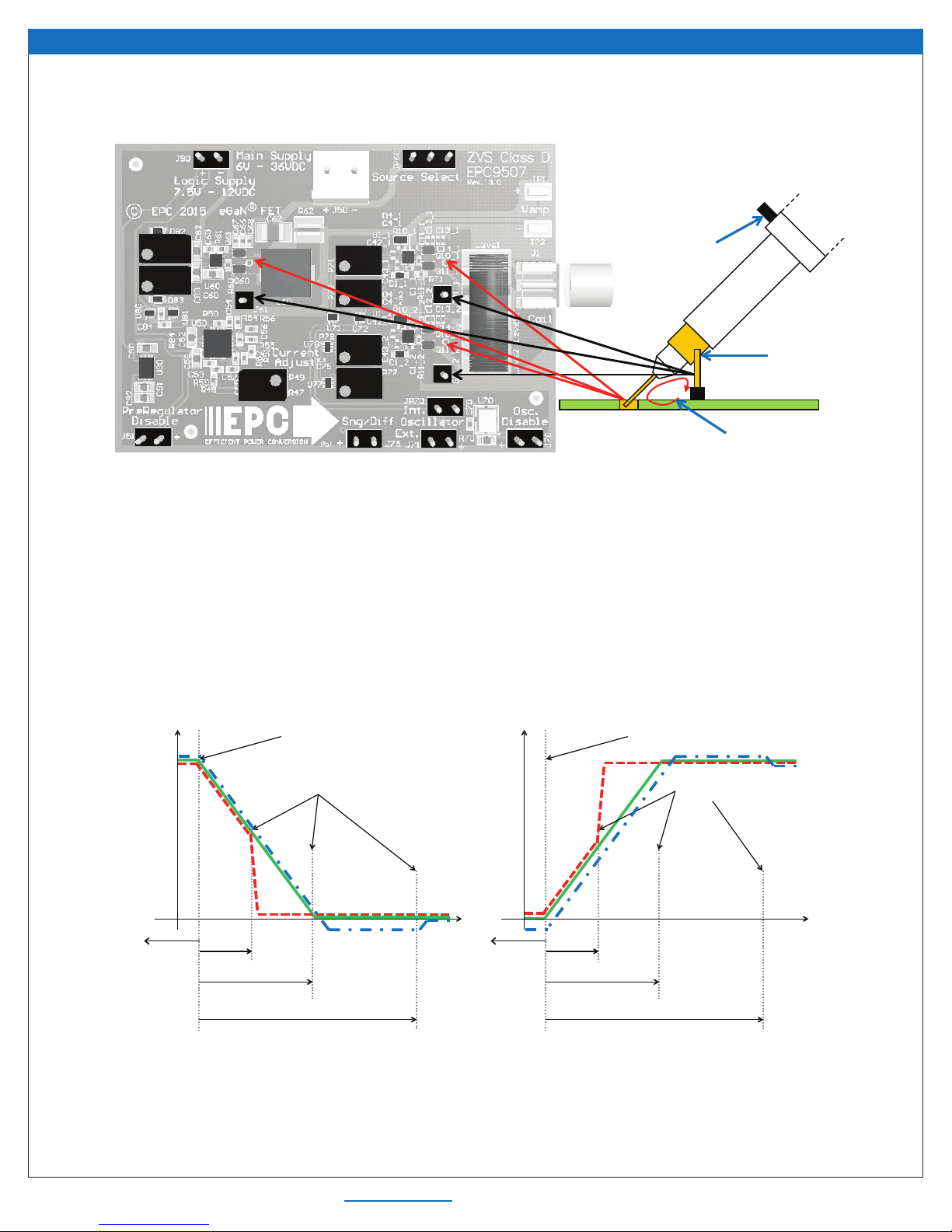
ZVS Timing Adjustment
Setting the correct time to establish ZVS transitions is critical to achieving
high eciency with the EPC9507 amplier. This can be done by selecting
the values for R71, R72, R77, and R78 respectively. This procedure is best
performed using potentiometers P71, P72, P77, and P78 installed that is
used to determine the xed resistor values. The procedure is the same for
both single ended and dierential mode of operation (as applicable per
operating mode). The timing MUST initially be set WITHOUT the source coil
connected to the amplier. The timing diagrams are given in Figure 4 and
should be referenced when following this procedure. Only perform these
steps if changes have been made to the board as it is shipped preset.
The steps are:
1. Remove the jumper in JP60 and insert it into J51 to place the EPC9507
amplier in bypass mode. With power o connect the main input
power supply (+) bus to the center pin of JP60 (pin 2) and the ground of
the main power to the ground (-) connection of J50 -VIN.
2. With power o, connect the control input power supply bus to +VDD
(J90). Note the polarity of the supply connector.
3. Connect a LOW capacitance oscilloscope probe to the probe-hole J2
between the two eGaN FETs Q10_x and Q11_x and lean against the
ground post as shown in Figure 3.
4. Turn on the control supply – make sure the supply is between 7V and 12
V range (7.5 V is recommended).
5. Turn on the main supply voltage to the required predominant
operating value (such as 24 V but NEVER exceed the absolute
maximum voltage of 36 V).
6. While observing the oscilloscope adjust P71 or P77 for the rising
edge of the waveform so achieve the green waveform of gure 4.
Repeat for the falling edge of the waveform by adjusting P72 or P78.
Repeat for the other eGaN FET pair if using dierential mode operation.
7. Check that the setting remains optimal with a source coil attached.
In this case it is important that the source coil is TUNED to resonance
WITH an applicable load. Theoretically the settings should remain
unchanged. Adjust if necessary.
8. Replace the potentiometers with xed value resistors. Congure the
EPC9507 amplier back to normal operation by removing the power
connections to J50 and JP60, removing the jumper in J51 and inserting
it back into JP60 (right 2 pins 2 & 3).
Determining Component Values for LZVS
The ZVS tank circuit is not operated at resonance, and only provides the
necessary negative device current for self-commutation of the output
voltage at turn o. The capacitance CZVS is chosen to have a very small
ripple voltage component and is typically around 1 µF. The amplier supply
voltage, switch-node transition time will determine the value of inductance
for LZVSx which needs to be sucient to maintain ZVS operation over the DC
device load resistance range and coupling between the device and source
coil range and can be calculated using the following equation:
(1)
LZVS = ∆tvt
8 ∙ fsw∙ COSSQ