LG 50PK550 User manual

PLASMA TV
SERVICE MANUAL
CAUTION
BEFORE SERVICING THE CHASSIS,
READ THE SAFETY PRECAUTIONS IN THIS MANUAL.
CHASSIS : PB01A
MODEL : 50PK550 50PK550-SA
North/Latin A erica http://aic.lgservice.co
Europe/Africa http://eic.lgservice.co
Asia/Oceania http://biz.lgservice.co
Internal Use Only
Printed in Korea
P/NO : MFL63141001(1005-REV00)

- 2 - LGE Internal Use OnlyCopyright ©2010 LG Electronics Inc. All rights reserved.
Only or training and service purposes
CONTENTS
CONTENTS ............................................................................................................................... 2
SAFETY PRECAUTIONS...........................................................................................................3
SPECIFICATION.........................................................................................................................4
ADJUSTMENT INSTRUCTION..................................................................................................6
BLOCK DIAGRAM ...................................................................................................................14
EXPLODED VIEW ...................................................................................................................15
SVC. S EET ................................................................................................................................

- 3 - LGE Internal Use OnlyCopyright ©2010 LG Electronics Inc. All rights reserved.
Only or training and service purposes
SAFETY PRECAUTIONS
Many electrical and mechanical parts in this chassis have special sa ety-related characteristics. These parts are identi ied by in
the Schematic Diagram and Exploded View.
It is essential that these special sa ety parts should be replaced with the same components as recommended in this manual to
prevent X-RADIATION, Shock, Fire, or other Hazards.
Do not modi y the original design without permission o manu acturer.
General Guidance
An isolation Transformer should always be used during the
servicing o a receiver whose chassis is not isolated rom the AC
power line. Use a trans ormer o adequate power rating as this
protects the technician rom accidents resulting in personal injury
rom electrical shocks.
It will also protect the receiver and it's components rom being
damaged by accidental shorts o the circuitry that may be
inadvertently introduced during the service operation.
I any use (or Fusible Resistor) in this monitor is blown, replace it
with the speci ied.
When replacing a high wattage resistor (Oxide Metal Film
Resistor, over 1W), keep the resistor 10mm away rom PCB.
Keep wires away rom high voltage or high temperature parts.
Due to high vacuum and large sur ace area o picture tube,
extreme care should be used in handling the Picture Tube.
Do not li t the Picture tube by it's Neck.
Leakage Current Cold Check(Antenna Cold Check)
With the instrument AC plug removed rom AC source, connect
an electrical jumper across the two AC plug prongs. Place the
AC switch in the on position, connect one lead o ohm-meter to
the AC plug prongs tied together and touch other ohm-meter
lead in turn to each exposed metallic parts such as antenna
terminals, phone jacks, etc.
I the exposed metallic part has a return path to the chassis, the
measured resistance should be between 1MΩ and 5.2MΩ.
When the exposed metal has no return path to the chassis the
reading must be in inite.
An other abnormality exists that must be corrected be ore the
receiver is returned to the customer.
Leakage Current ot Check (See below Figure)
Plug the AC cord directly into the AC outlet.
Do not use a line Isolation Transformer during this check.
Connect 1.5K/10watt resistor in parallel with a 0.15uF capacitor
between a known good earth ground (Water Pipe, Conduit, etc.)
and the exposed metallic parts.
Measure the AC voltage across the resistor using AC voltmeter
with 1000 ohms/volt or more sensitivity.
Reverse plug the AC cord into the AC outlet and repeat AC
voltage measurements or each exposed metallic part. Any
voltage measured must not exceed 0.75 volt RMS which is
corresponds to 0.5mA.
In case any measurement is out o the limits speci ied, there is
possibility o shock hazard and the set must be checked and
repaired be ore it is returned to the customer.
Leakage Current ot Check circuit
1.5 Kohm/10W
To Instrument's
exposed
METALLIC PARTS
Good Earth Ground
such as WATER PIPE,
CONDUIT etc.
AC Volt-meter
IMPORTANT SAFETY NOTICE
0.15uF

- 4 - LGE Internal Use OnlyCopyright ©2010 LG Electronics Inc. All rights reserve .
Only for training an service purposes
SPECIFICATIONS
NOTE : Specifications an others are subject to change without notice for improvement
.
1. Application Range
(1) This spec sheet is applie all of PDP TV with PB01A chassis.
2. Specification
Each part is teste as below without special appointment.
(1) Temperature : 25 °C ± 5 °C (77 °F ± 9 °F), CST : 40 °C ± 5 °C
(2) Relative Humi ity : 65 % ± 10 %
(3) Power Voltage : Stan ar input voltage (100 V - 240 V ~ 50 / 60 Hz)
* Stan ar Voltage of each pro uct is marke by mo els
(4) Specification an performance of each parts are followe each rawing an specification by part number in accor ance with
BOM.
(5) The receiver must be operate for about 5 minutes prior to the a justment.
3. Test Method
(1) Performance : LGE TV test metho followe .
(2) Deman e other specification
Safety: UL, CSA, IEC specification, CE
EMC : FCC, ICES, IEC specification, CE
Mo el Name Market Bran
50PK550-SA Brazil LG
Mo el Name Market Appliance
50PK550-SA Brazil Safety : IEC/EN60065

- 5 - LGE Internal Use OnlyCopyright ©2010 LG Electronics Inc. All rights reserved.
Only or training and service purposes
4. General Specification
No Item Speci ication Model Remark
1. Receiving System 1) SBTVD / NTSC / PAL-M / PAL-N PK550, PK950
2) NTSC / PAL-M / PAL-N PK950R Analog model
2. Available Channel 1) VHF : 02~13 PK550, PK950
2) UHF : 14~69
3) DTV : 07-69 (VHF high/UHF)
4) CATV : 02~135
1) VHF : 02~13 PK950R Analog model
2) UHF : 14~69
3) CATV : 02~135
3. Input Voltage 1)AC 100 V ~ 240 V 50 / 60 Hz
4. Market BRAZIL PK550, PK950
Latin America PK950R
5. Screen Size 50 inch Wide(1920 X1080) 50PK550-SA, 50PK950-SA
50PK950R-MA
60 inch Wide(1920 X 1080) 60PK550-SA, 60PK950-SA
6. Aspect Ratio 16:9 60PK950R-MA
7. Tuning System FS
8. Module PDP50R1#### (1920 X 1080) 50PK550-SA, 50PK950-SA
50PK950R-MA
PDP60R1#### (1920 X 1080) 60PK550-SA, 60PK950-SA
60PK950R-MA
9. Operating Environment 1) Temp : 0 deg ~ 40 deg
2) Humidity : ~ 80 %
10. Storage Environment 1) Temp : -20 deg ~ 60 deg
2) Humidity : 0 % ~ 90 %

- 6 - LGE Internal Use OnlyCopyright ©2010 LG Electronics Inc. All rights reserved.
Only or training and service purposes
ADJUSTMENT INSTRUCTION
1. Application Range
This spec. sheet applies to PB01A Chassis applied PDP TV
all models manu actured in TV actory.
2. Specification
(1) Because this is not a hot chassis, it is not necessary to use
an isolation trans ormer. However, the use o isolation
trans ormer will help protect test instrument.
(2) Adjustment must be done in the correct order. But it is
lexible when its actory local problem occurs.
(3) The adjustment must be per ormed in the circumstance o
25 cC ± 5 cC o temperature and 65 % ± 10 % o relative
humidity i there is no speci ic designation.
(4) The input voltage o the receiver must keep 100 V - 240 V,
50 / 60 Hz.
(5) Be ore adjustment, execute Heat-Run or 5 minutes.
VA ter Receive 100% Full white pattern (06CH) then
process Heat-run
(or “8. Test pattern” condition o Ez-Adjust status)
VHow to make set white pattern
1) Press Power ON button o Service Remocon
2) Press ADJ button o Service remocon. Select “10.
Test pattern” and, a ter select “White” using
navigation button, and then you can see 100% Full
White pattern.
* In this status you can maintain Heat-Run useless any
pattern generator
* Notice: i you maintain one picture over 20 minutes
(Especially sharp distinction black with white pattern –
13Ch, or Cross hatch pattern – 09Ch) then it can
appear image stick near black level.
3. Adjustment items
3-1. PCB Assembly adjustment
(1) Adjust 480i Comp1
(2) Adjust 1080p Comp1/RGB
- I it is necessary, it can adjustment at Manu acture Line
- You can see set adjustment status at “9. ADJUST
CHECK” o the “In-start menu”
3-2. Set Assembly Adjustment
(1) EDID (The Extended Display Identi ication Data )
(2) Color Temperature (White Balance) Adjustment
(3) Make sure RS-232C control
(4) Selection Factory output option
4. PCB Assembly Adjustment
4-1. Using RS-232C
- Adjust 3 items at 3-1 PCB assembly adjustments
“ (3) Adjustment sequence” one a ter the order.
(1) Adjustment protocol
(2) Necessary items be ore Adjustment items
OPattern Generator : (MSPG-925FA)
OAdjust 480i Comp1
(MSPG-925FA:model :209, pattern :65) – Comp1 Mode
OAdjust 1080p Comp1
(MSPG-925FA:model :225 , pattern :65) – Comp1 Mode
OAddjust RGB (MSPG-925FA:model :225 , pattern :65)
– RGB-PC Mode
* I you want more in ormation then see the below Adjustment
method (Factory Adjustment)
(3) Adjustment sequence
Oaa 00 00: Enter the ADC Adjustment mode.
Oxb 00 40: Change the mode to Component1 (No actions)
Oad 00 10: Adjust 480i Comp
Oad 00 10: Adjust 1080p comp
Oxb 00 60: Change to RGB-PC mode(No action)
Oad 00 10: Adjust 1080p RGB
Oxb 00 90: Endo o Adjustmennt
< See ADC Adjustment RS232C Protocol_Ver1.0 >

5. Factory Adjustment
PB01A : USE EXTERNAL ADC(BCM) : using instrument.
PB02A : USE NTERNAL ADC(S7) : using internal pattern.
5-1. Auto Adjust Component
480i/1080p RGB 1080p
(1) Summary : Adjustment component 480i/1080i and RGB
1080p is Gain and Black level setting at Analog
to Digital converter, and compensate the RGB
deviation
(2) Using instrument
1) Adjustment remocon, 801GF(802B, 802F, 802R) or
MSPG925FA pattern generator
( t can output 480i/1080i horizontal 100 % color bar
pattern signal, and its output level must setting
0.7 V ± 0.1 V p-p correctly)
* You must make it sure its resolution and pattern cause every
instrument can have different setting
2) Adjustment method 480i Comp1, Adjust 1080p
Comp1/RGB (Factory adjustment)
O ADC 480i Component1 adjustment -
- Check connection of Component1
- MSPG-925FA Ë Model: 209, Pattern 65
OSet Component 480i mode and 100% Horizontal
Color Bar Pattern(HozTV31Bar), then set TV set to
Component1 mode and its screen to “NORMAL”
OADC 1080p Component1 / RGB adjustment
- Check connection both of Component1 and RGB
- MSPG-925FA Ë Model: 225, Pattern 65
OSet Component 1080p mode and 100% Horizontal
Color Bar Pattern(HozTV31Bar), then set TV set to
Component1 mode and its screen to “NORMAL”
OAfter get each the signal, wait more a second and
enter the “ N-START” with press N-START key of
Service remocon. After then select “7. External ADC”
with navigator button and press “Enter”.
OAfter Then Press key of Service remocon “Right
Arrow(VOL+)”
OYou can see “ADC Component1 Success”
OComponent1 1080p, RGB 1080p Adjust is same
method.
OComponent 1080p Adjustment in Component1 input
mode
ORGB 1080p adjustment in RGB input mode
Of you success RGB 1080p Adjust. You can see “ADC
RGB-DTV Success”
Caution : Set Volume 0 after adjustment
5-2. se Internal ADC(S7)
- ADJ(EZ ADJUST) -> 6.ADC Calibration -> ADC
Calibration(START)
5-3. EDID(The Extended Display
Identification Data) / DDC(Display Data
Channel) download
(1) Summary
1) t is established in VESA, for communication between
PC and Monitor without order from user for building user
condition. t helps to make easily use realize “Plug and
Play” function.
2) For ED D data write, we use DDC2B protocol.
5-4. Auto Download
(1) After enter Service Mode by pushing “ADJ” key,
(2) Enter ED D D/L mode.
(3) Enter “START” by pushing “OK” key.
Caution
- Never connect HDM & D-sub Cable when the user
downloading .
- Use the proper cables below for ED D Writing.
- 7 - LGE nternal Use OnlyCopyright ©2010 LG Electronics nc. All rights reserved.
Only for training and service purposes
< Adjustment pattern : 480i / 1080p 60Hz Pattern >

* Edid data and Model option download(RS232)
5-5. Manual Download
(1) Write HDM ED D data
1) Using instruments
- Jig. (PC Serial to D-Sub connection) for PC, DDC
adjustment.
- S/W for DDC recording (ED D data write and read)
- D-sub jack
- Additional HDM cable connection Jig.
2) Preparing and setting.
- Set instruments and Jig. Like pic.5), then turn on PC
and Jig.
- Operate DDC write S/W (ED D write & read)
- t will operate in the DOS mode.
- ED D data (Model name = LG TV)
- 2010 ED D DATA CHECK SUM.
- 8 - LGE nternal Use OnlyCopyright ©2010 LG Electronics nc. All rights reserved.
Only for training and service purposes
BLOCK(0) BLOCK(1)
HD HDM 1 3B 2C
HDM 2 3B 1C
HDM 3 3B 0C
RGB A3
FHD HDM 1 3B 2C
HDM 2 3B 1C
HDM 3 3B 0C
HDM 4 3B FC
RGB A3
< For write ED D data, setting Jig and another instruments >

- 9 - LGE nternal Use OnlyCopyright ©2010 LG Electronics nc. All rights reserved.
Only for training and service purposes
* See Working Guide if you want more information about ED D
communication.
5-6. Adjustment Color Temperature
(White balance)
(1) Using nstruments
1) Color Analyzer: CA-210 (CH 9)
- Using LCD color temperature, Color Analyzer (CA-210)
must use CH 9, which Matrix compensated (White,
Red, Green, Blue compensation) with CS-2100. See
the Coordination bellowed one.
2) Auto-adjustment Equipment ( t needs when Auto-
adjustment – t is availed communicate with RS-232C :
Baud rate: 115200)
3) Video Signal Generator MSPG-925F 720p, 216Gray
(Model: 217, Pattern 78)
(2) Connection Diagram (Auto Adjustment)
1) Using nner Pattern
2) Using HDM input
(3) White Balance Adjustment
- f you can’t adjust with inner pattern, then you can adjust it
using HDM pattern. You can select option at “Ez-Adjust
Menu – 7. White Balance” there items “NONE, NNER,
HDM ”. t is normally setting at inner basically. f you can’t
adjust using inner pattern you can select HDM item, and
you can adjust.
- n manual Adjust case, if you press ADJ button of service
remocon, and enter “Ez-Adjust Menu – 7. White Balance”,
then automatically inner pattern operates. ( n case of
“ nner” originally “Test-Pattern. On” will be selected in The
“Test-Pattern. On/Off”.
OConnect all cables and equipments like Pic.5)
OSet Baud Rate of RS-232C to 115200. t may set
115200 orignally.
OConnect RS-232C cable to set
OConnect HDM cable to set
V RS-232C COMMAND(Commonly apply)
< Connection Diagram for Adjustment White balance >
RS-232C COMMAND
[CMD D DATA] Meaning
wb 00 00 White Balance adjustment start.
wb 00 10 Start of adjust gain
( nner white pattern)
wb 00 1f End of gain adjust
wb 00 20 Start of offset adjust
( nner white pattern)
wb 00 2f End of offset adjust
wb 00 ff End of White Balance adjust
( nner pattern disappeared)

- 10 - LGE nternal Use OnlyCopyright ©2010 LG Electronics nc. All rights reserved.
Only for training and service purposes
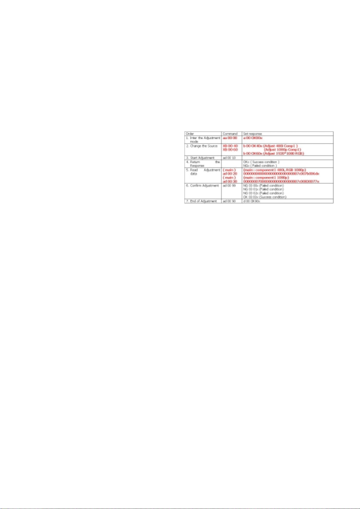
O wb 00 00”: Start Auto-adjustment of white balance.
O“wb 00 10”: Start Gain Adjustment ( nner pattern)
O“jb 00 c0” :
O…
O“wb 00 1f”: End of Adjustment
* f it needs, offset adjustment (wb 00 20-start, wb 00 2f-
end)
O“wb 00 ff”: End of white balance adjustment (inner pattern
disappear)
V Adjustment Mapping information
OWhen Color temperature (White balance) Adjustment
(Automatically)
- Press “Power only key” of service remocon and
operate automatically adjustment.
- Set BaudRate to 115200.
OYou must start “wb 00 00” and finish it “wb 00 ff”.
Of it needs, then adjustment “Offset”.
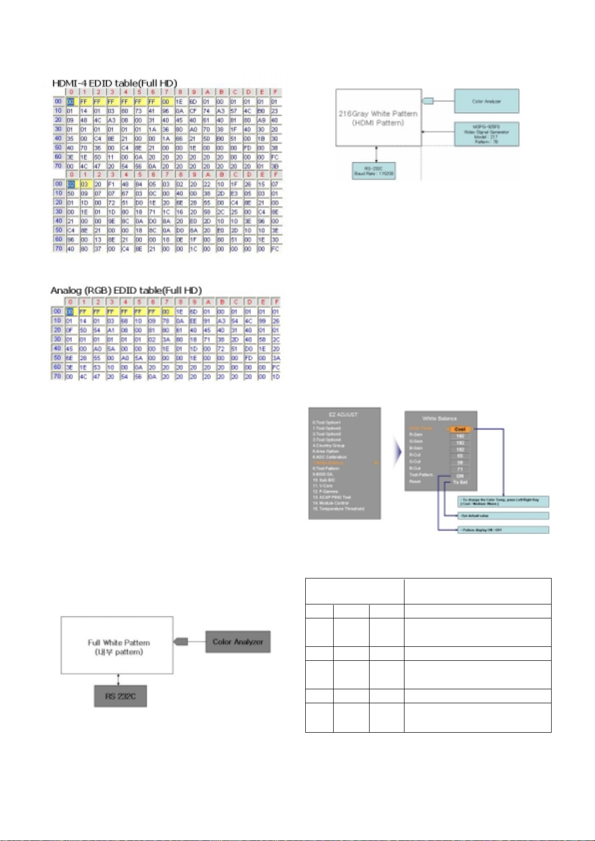
(4) White Balance Adjustment (Manual adjustment)
1) Test Equipment: CA-210
- Using PDP color temperature, Color Analyzer (CA-210)
must use CH 10, which Matrix compensated (White,
Red, Green, Blue compensation) with CS-2100. See
the Coordination bellowed one.
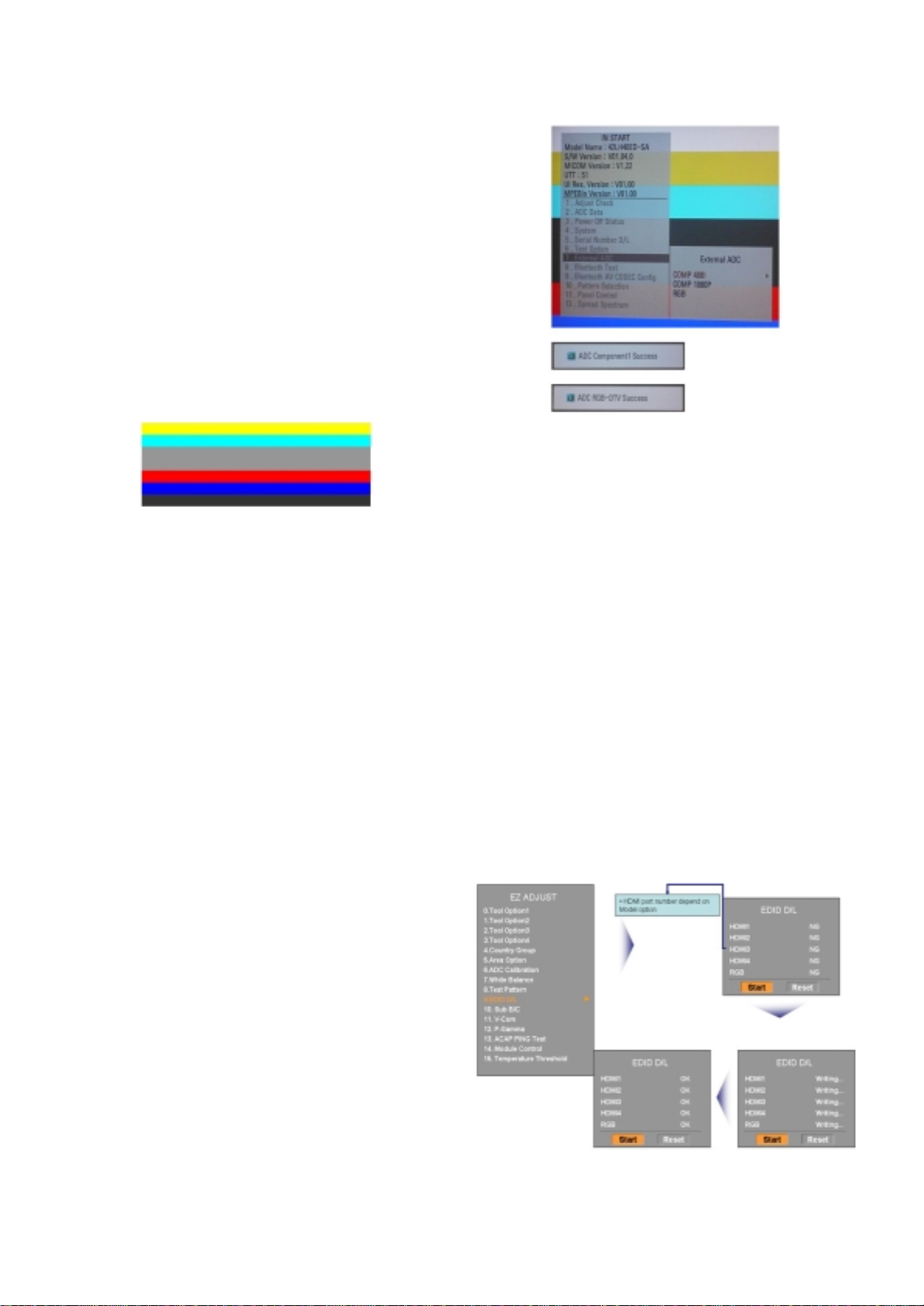
2) Manual adjustment sequence is like bellowed one.
- Turn to “Ez-Adjust” mode with press ADJ button of
service remocon.
- Select “10.Test Pattern” with CH+/- button and press
enter. Then set will go on Heat-run mode. Over 30
minutes set let on Heat-run mode.
- Let CA-210 to zero calibration and must has gap more
10cm from center of PDP module when adjustment.
- Press “ADJ” button of service remocon and select
“7.White-Balance” in “Ez-Adjust” then press “G” button
of navigation key. (When press “G” button then set will
go to full white mode)
- Adjust at three mode (Cool, Medium, Warm)
- f “cool” mode
Let B-Gain to 192 and R, G, B-Cut to 64 and then
control R, G gain adjustment High Light adjustment.
- f “Medium” and “Warm” mode Let R-Gain to 192 and
R, G, B-Cut to 64 and then control G, B gain
adjustment High Light adjustment.
- All of the three mode
Let R-Gain to 192 and R, G, B-Cut to 64 and then
control G, B gain adjustment High Light adjustment.
- With volume button (+/-) you can adjust.
- After all adjustment finished, with Enter (_ key) turn to
Ez-Adjust mode. Then with ADJ button, exit from
adjustment mode
* Attachment: White Balance adjustment coordination and color
temperature.
OUsing CS-1000 Equipment.
- COOL : T=11000K, _uv=0.000, x=0.276 y=0.283
- MED UM : T=9300K, _uv=0.000, x=0.285 y=0.293
- WARM : T=6500K, _uv=0.000, x=0.313 y=0.329
OUsing CA-210 Equipment. (10 CH)
- Contras value : 216 Gray
- Brighness spec.
6. Test of RS-232C control.
- Press n-Start button of Service Remocon then set the “4.Baud
Rate” to 115200. Then check RS-232C control and
7. Selection of Country option.
- Selection of country option is allowed only North American
model (Not allowed Korean model). t is selection of Country
about Rating and Time Zone.
(1) Models: All models which PB82C Chassis (See the first
page.)
(2) Press “ n-Start” button of Service Remocon, then enter the
“Option” Menu with “P P CH-“ Button
(3) Select one of these three (USA, CANADA, MEX CO)
defends on its market using “Vol. +/-“button.
Caution : Don’t push The NSTOP KEY after completing the
function inspection
Caution : nspection only PAL M
RS-232C COMMAND
CENTER
[CMD D DATA] M N (DEFAULT) MAX
Cool Mid Warm Cool Mid Warm
R Gain jg Ja jd 00 184 192 192 192
G Gain jh Jb je 00 187 183 159 192
B Gain ji Jc jf 00 192 161 95 192
R Cut 64 64 64 127
G Cut 64 64 64 127
B Cut 64 64 64 127
Color Test Color Coordination
temperature Equipment x y
COOL CA-210 0.276±0.002 0.283±0.002
MED UM CA-210 0.285±0.002 0.293±0.002
WARM CA-210 0.313±0.002 0.329±0.002
tem Min Typ Max Unit Remark
White 49 60 - cd/m - 100%Window White
average Pattern
brightness - 100 RE(255Gray)
- Picture: Vivid(Medium )
Brightness -20 +20 % - 85 RE(216Gray) 100%
uniformity Window White Pattern
- Picture: Vivid(Medium)

8. MAC Address and ESN Key Write
8-1. Equipment & Condition
- Play ile: Serial.exe
- MAC Address edit
- Input Start / End MAC address
8-2. Download method
(1) Communication Prot connection
Connect: PCBA Jig-> RS-232C Port== PC-> RS-232C Port
(2) MAC Address Download
- Com 1,2,3,4 and 115200(Baudrate)
- Port connection button click(1)
- Load button click(2) or MAC Address write.
- Start MAC Address write button(3)
- Check the OK Or NG
8-3. Equipment & Condition
- Each other connection to LAN Port o IP Hub and Jig
8-4. MAC Address
- Push “IN-START” Key in service remote controller.
- Check ESN KEY only north America model
8-5. LAN PORT INSPECTION(PING TEST)
- LAN Port connection with PCB
- Network setting at MENU Mode o TV
- setting automatic IP
- Setting state con irmation
-> I automatic setting is inished, you con irm IP and MAC
Address.
- remove LAN CABLE
9. GND and ESD Testing
9-1. Prepare GND and ESD Testing.
- Check the connection between set and power cord
9-2. Operate GND and ESD auto-test.
(1) Fully connected (Between set and power cord) set enter
the Auto-test sequence.
(2) Connect D-Jack AV jack test equipment.
(3) Turn on Auto-controller(GWS103-4)
(4) Start Auto GND test.
(5) I its result is NG, then notice with buzzer.
(6) I its result is OK, then automatically it turns to ESD Test.
(7) Operate ESD test
(8) I its result is NG, then notice with buzzer.
(9) I its result is OK, then process next steps. Notice it with
Good lamp and STOPER Down.
9-3. Check Items.
(1) Test Voltage
GND: 1.5KV/min at 100mA
Signal: 3KV/min at 100mA
(2) Test time: just 1 second.
(3) Test point
GND test: Test between Power cord GND and Signal cable
metal GND.
ESD test: Test between Power cord GND and Live and
neutral.
(4) Leakage current: Set to 0.5mA(rms)
- 11 - LGE Internal Use OnlyCopyright ©2010 LG Electronics Inc. All rights reserved.
Only or training and service purposes

10. POWER PCB Ass’y Voltage
Adjustment
(Va/Vs Voltage Adjustment)
(1)Test equipment : D.M.M 1EA
(2) Connection Diagram for Measuring : refer to fig.1
10-1. Adjustment met od
(1) Vs adjustment (refer fig.1)
1) Connect terminal of D.M.M. to Vs pin of
P812(42”:P811), connect -terminal to GND pin of
P812(42”:P811)
2) After turning VR901, voltage of D.M.M adjustment as
same as Vs voltage which on label of panel left/top (
deviation ; ±0.5V)
(2) Va adjustment (refer fig.1)
1) After receiving 100% Full White Pattern, HEAT RUN.
2) Connect terminal of D.M.M. to Va pin of
P812(42”:P811), connect -terminal to GND pin of
P811(42”:P812).
3) After turning VR502,voltage of D.M.M adjustment as
same as Va voltage which on label of panel left/top
(deviation; ±0.5V)
11. Default Service option.
11-1. ADC-Set.
VR-Gain adjustment Value (default 128)
VG-Gain adjustment Value (default 128)
VB-Gain adjustment Value (default 128)
VR-Offset adjustment Value (default 128)
VG-Offset adjustment Value (default 128)
VB-Offset adjustment Value (default 128)
11-2. W ite balance. Value.
11-3. Temperature T res old
VThreshold Down Low 20
VThreshold Up Low 23
VThreshold Down High 70
VThreshold Up High 75
11. USB DOWNLOAD
(*.epk file download)
VPut the USB Stick to the USB socket
VPress Menu key, and move OPTION
VPress “FAV” Press 7 times.
- 12 - LGE Internal Use OnlyCopyright ©2010 LG Electronics Inc. All rights reserved.
Only for training and service purposes
< fig.1 : 50 FHD Power PCB Assy Voltage adjustment >
CENTER (DEFAULT)
Cool Mid Warm
R Gain 192 192 192
G Gain 192 192 192
B Gain 192 192 192
R Cut 64 64 64
G Cut 64 64 64
B Cut 64 64 64

VSelect download ile (epk ile)
VA ter download is inished, remove the USB stick.
V Press “IN-START” key o ADJ remote control, check the
S/W version.
CAUTION
- DO NOT REMOVE USB MEMORY CARD FROM USB PORT
WHEN YOU FIND BELOW DESCRIPTION
- " Do not remove the memory card rom the port! "
- 13 - LGE Internal Use OnlyCopyright ©2010 LG Electronics Inc. All rights reserved.
Only or training and service purposes

- 14 - LGE Internal Use OnlyCopyright ©2010 LG Electronics Inc. All rights reserved.
Only or training and service purposes
BLOCK DIAGRAM

- 15 - LGE Internal Use Only
EXPLODED VIEW
Copyright ©2010 LG Electronics Inc. All rights reserved.
Only for training and service purposes
400
602 601
520
900
305
300 301
302
303
501 590
200
580
205
202
203
208
209
204
206
207
201
240
604
120
302
910
Many electrical and mec anical parts in t is c assis ave special safety-related c aracteristics. T ese
parts are identified by in t e Sc ematic Diagram and EXPLODED VIEW.
It is essential t at t ese special safety parts s ould be replaced wit t e same components as
recommended in t is manual to prevent X-RADIATION, S ock, Fire, or ot er Hazards.
Do not modify t e original design wit out permission of manufacturer.
IMPORTANT SAFETY NOTICE
A10 A9
LV1
A12
A21
A2

THE SYMBOL MARK OF THIS SCHEMETIC DIAGRAM INCORPORATES
SPECIAL FEATURES IMPORTANT FOR PROTECTION FROM X-RADIATION.
FILRE AND ELECTRICAL SHOCK HAZARDS, WHEN SERVICING IF IS
ESSENTIAL THAT ONLY MANUFATURES SPECFIED PARTS BE USED FOR
THE CRITICAL COMPONENTS IN THE SYMBOL MARK OF THE SCHEMETIC.
USB1_DM_to_HUB 100K
R1109
READY
USB1_DP_to_HUB
USB2_DM_to_HUB
0.1uF
16V
C1118
PK950
USB_DM
USB2_DP_to_HUB
0.1uF
16V
C1112
READY
USB_DP
USB2_DP_to_HUB
USB2_DM_to_HUB
10K
R1119
PK950
10K
READY
R1129
USB1_DM_to_HUB
10K
R1120
0
PK950
R1126 USB1_DP_to_HUB
10K
READY
R1130
0.1uF
16V
C1119
USB1_OCD
0
PK950
R1125
0
PK550
R1123
USB1_CTL
0
PK550
R1124
BT_DP_T
BT_DM_T
RTR030P02
Q1101
PK950
S
D
G
BT_ON/OFF
4.7K
R1113
PK950
0
READY
R1110
2SC3052
Q1100
PK950
E
B
C
4.7K
R1112
PK950
47K
R1111
PK950
0R1132
PK550
USB1_CTL_HUBUSB1_OCD_HUB
0R1127
PK950
USB2_CTL_HUB
USB2_OCD_HUB
USB1_OCD_HUB
USB1_CTL_HUB
USB2_OCD_HUB
USB2_CTL_HUB
/RST_HUB 001:H1
MAERTSNWODBSU
KJA-UB-4-0004
EAG41945401
JK1100
1
2
3
4
5
MAERTSNWODBSU
KJA-UB-4-0004
EAG41945401
JK1101
PK950
1
2
3
4
5
BT_RESET
VREG_CTR
AP2191SG-13
IC1101
PK950
3IN_2
2IN_1
4EN
1GND
5
FLG
6
OUT_1
7
OUT_2
8
NC
AP2191SG-13
IC1102
3IN_2
2IN_1
4EN
1GND
5
FLG
6
OUT_1
7
OUT_2
8
NC
BT_USB_DM
BT_USB_DP
100uF
16V
C1116
100uF
16V
C1117
100uF
16V
C1115
PK950
100uF
16V
C1114
PK950
100K R1107
0. 1 u F C1109
100K R1106
0. 1 u F C1101
0. 1 u F C1100
1uF C1104
0. 1 u F C1103
1M
R1102
4.7uF
C1110
0. 1 u F C1111
12K R1101
1uF C1106
0. 1 u F C1107
100K R1104
D3.3V
0. 1 u F C1102
100K R1108
0 R1100
15pF
50V
C1108
15pF
50V
C1105
4.7K
R1105
D3.3V
D3.3V
D3.3V D3.3V
D3.3V D3.3V
12507WR-10L
P1102
PK950
1
2
3
4
5
6
7
8
9
10
11
100K
R1133
THERMAL
USB2512A_AEZG
IC1100
PK950
1
USBDN1_DM
3
USBDN2_DM
7
NC_2
9
NC_4
10
VDDA33_2
11
TEST
12
PRTPWR1
13
OCS1_N
14
VDD18
15
VDD33CR
16
PRTPWR2
17
OCS2_N
18
NC_5
19 NC_6
20 NC_7
21 NC_8
22 SDA/SMBDATA/NON_REM1
23 VDD33
24 SCL/SMBCLK/CFG_SEL0
25 HS_IND/CFG_SEL1
26 RESET_N
27 VBUS_DET
28 0MER_NON/RWP_LACOL/DNI_PSUS
29 VDDA33_3
30 USBUP_DM
31 USBUP_DP
32 XTAL2
5
VDDA33_1
8
NC_3
6
NC_1
4
USBDN2_DP
2
USBDN1_DP
33 XTAL1/CLKIN
34 VDD18PLL
35 RBIAS
36 VDD33PLL
37
VSS
24MHz
X1100
0R1115
PK950
0R1131
PK950
P_+5V
P_+5V
1uF
C1113
PK950
BT_DP
BT_DM
0
PK950
R1142
0
PK950
R1143
0
PK550
R1144
0
PK550
R1145
BT_DP_T
BT_DM_T
BT_USB_DM
BT_USB_DP
0R1118
PK550
0
R1141
PK950
0R1140
PK950
0 R1103
USB2 SIDE UNDER
SWITCHADDED
Capacitors on VBUSA should be
placed as closd to connector as possible.
USB2 Dato to USB2512
Capacitors on VBUSA should be
placed as closd to connector as possible.
SWITCHADDED
USB1 Dato to MAIN(BCM)
USB1 Dato to USB2512
USB1 SIDE UPPER
USB HUB
1 3 1 3
BLUETOOTH
BLUETOOTH
USB HUB
EAX61354901
CLOSE TO BCM3556
Copyright © 2010 LG Electronics Inc. All rights reserved.
Only for training and service purposes
LGE Internal Use Only

THE SYMBOL MARK OF THIS SCHEMETIC DIAGRAM INCORPORATES
SPECIAL FEATURES IMPORTANT FOR PROTECTION FROM X-RADIATION.
FILRE AND ELECTRICAL SHOCK HAZARDS, WHEN SERVICING IF IS
ESSENTIAL THAT ONLY MANUFATURES SPECFIED PARTS BE USED FOR
THE CRITICAL COMPONENTS IN THE SYMBOL MARK OF THE SCHEMETIC.
SPDIF_OUT
SIDE_RIN
SIDE_LIN
COMPOSITE2_IN
SIDEAV_DET
D3.3V
100pF
C1011
READY
1uF
25V
C1026
27pF
50V
C1030
5.1V
ZD1023
100pF
C1010
READY
100pF
C1032
READY
5.1V
ZD1029
470K
R1021
COMP1_Pr
003:B3
2.7K
R1012
5.1V
ZD1008
270nH
L1005
COMP2_Pb
003:B4
1uF
25V
C1015
5.1V
ZD1013
470K
R1006
COMP_L_IN_1
002:A5
5.1V
ZD1030
100pF
50V
C1028
27pF
50V
C1025
5.1V
ZD1020
COMP2_Pr
003:B3
5.1V
ZD1028
470K
R1015
COMP1_SW
001:H3
COMPOSITE1_IN
003:B4
PPJ237-0 1
JK1001
5 J [GN3]O-SPRING
6 J [GN3]E-LUG
4 J [GN3]CONTACT
7K [BL3]E-LUG-S
5K [BL3]O-SPRING
7L [RD3]E-LUG-S
5L [RD3]O-SPRING_1
5M [WH3]O-SPRING
4N [RD3]CONTACT
5N [RD3]O-SPRING_2
6N [RD3]E-LUG
6D [GN2]E-LUG
5D [GN2]O-SPRING
4D [GN2]CONTACT
7E [BL2]E-LUG-S
5E [BL2]O-SPRING
7F [RD2]E-LUG-S
5F [RD2]O-SPRING_1
5G [WH2]O-SPRING
4H [RD2]CONTACT
5H [RD2]O-SPRING_2
6H [RD2]E-LUG
6A [YL1]E-LUG
5A [YL1]O-SPRING
4A [YL1]CONTACT
5B [WH1]O-SPRING
4C [RD1]CONTACT
5C [RD1]O-SPRING
6C [RD1]E-LUG
270nH
L1000
5.1V
ZD1007
5.1V
ZD1011
5.1V
ZD1031
27pF
50V
C1014
5.1V
ZD1015
5.1V
ZD1009
1uF
25V
C1003
27pF
50V
C1019
COMP_R_IN_1
002:A5
COMPOSITE1_SW
001:H2
27pF
50V
C1018
5.1V
ZD1019
COMP2_Y
003:B3
COMP_L_IN_2
002:A5
5.1V
ZD1026
10
R1027
470K
R1022
5.1V
ZD1022
COMP_R_IN_2
002:A5
100pF
C1033
READY
COMP1_Pb
003:B3
2.7K
R1024
5.1V
ZD1017
100pF
50V
C1017
270nH
L1002
27pF
50V
C1031
270nH
L1004
1uF
25V
C1004
5.1V
ZD1012
27pF
50V
C1013
470K
R1014
1K
R1019
100pF
C1021
READY
10
R1020
27pF
50V
C1029
COMP1_Y
003:B3
1uF
25V
C1027
5.1V
ZD1014
27pF
50V
C1023
100pF
50V
C1007
270nH
L1003
27pF
50V
C1020
27pF
50V
C1012
2.7K
R1018
5.1V
ZD1021
AV_L_IN_1
002:A5
5.1V
ZD1024
5.1V
ZD1016
5.1V
ZD1006
100pF
C1022
READY
47pF
50V
C1006
27pF
50V
C1024
5.1V
ZD1018
270nH
L1001
1K
R1013
AV_R_IN_1
002:A5
1uF
25V
C1016
1K
R1026
470K
R1007
5.1V
ZD1010
5.1V
ZD1027
COMP2_SW
001:H3
5.1V
ZD1025
5.1V
ZD1004
5.1V
ZD1000
5.1V
ZD1002
2.7K
R1002
PPJ235-01
JK1000
4A [YL]O-SPRING
5A [YL]E-LUG
3A [YL]CONTACT
4B [WH]O-SPRING
3C [RD]CONTACT
4C [RD]O-SPRING
5C [RD]E-LUG
1K
R1003
100pF
C1009
READY
1uF
25V
C1001
470K
R1000
47pF
50V
C1005
1uF
25V
C1002
5.1V
ZD1003
100pF
50V
C1000
470K
R1001
5.1V
ZD1001
5.1V
ZD1005
100pF
C1008
READY
D3.3V
D3.3V
D3.3V
D3.3V
5.1V
ZD1032
5.1V
ZD1033
5.1V
ZD1034
5.1V
ZD1035
5.1V
ZD1036
5.1V
ZD1037
5.1V
ZD1038
5.1V
ZD1039 0.1uF
50V
C1034
10uF
16V
C1035
READY
22pF
C1036
NL17SZ00DFT2G
IC1000
READY
3
GND
2
B
4Y
1
A5VCC
citpOrebiF
JST1223-001
JK1002
1
GND
2
VCC
3
VINPUT
4
FIX_POLE
100
R1029
100
R1030
READY
1K
R1028
READY
D3.3V
COMP1_SW
9 1 3
EAX61354901
JACK
SPDIF
AV 1
COMPONENT1/2,AV1
COMPONENT2
COMPONENT1
SIDE_AV
NAND
GATE
Copyright © 2010 LG Electronics Inc. All rights reserved.
Only for training and service purposes
LGE Internal Use Only

THE SYMBOL MARK OF THIS SCHEMETIC DIAGRAM INCORPORATES
SPECIAL FEATURES IMPORTANT FOR PROTECTION FROM X-RADIATION.
FILRE AND ELECTRICAL SHOCK HAZARDS, WHEN SERVICING IF IS
ESSENTIAL THAT ONLY MANUFATURES SPECFIED PARTS BE USED FOR
THE CRITICAL COMPONENTS IN THE SYMBOL MARK OF THE SCHEMETIC.
DSUB_DET
DDC_SDA
DDC_SCL
100
R930
0.1uF
50V
C915
+3.3V_ST
0.1uF
50V
C918
0.1uF
50V
C919
MAX3232CDR
IC902
3-1C
2+V
4+2C
1+1C
6-V
5-2C
72TUOD
82NIR
9
2TUOR
01
2NID
11
1NID
21
1TUOR
31
1NIR
41
1TUOD
51
DNG
61
CCV
0.1uF
50V
C920
100
R931
RS232C_TXD
+3.3V_ST
RS232C_RXD
0.1uF
50V
C914
PC_L_IN
PC_R_IN
KEY2
+3.3V_ST
KEY1
LED_WHITE
ADUC30S03010L_AMODIODE
30V
READY
D910
ADUC30S03010L_AMODIODE
30V
READY
D911
LED_BREATHING
MLB-201209-0120P-N2
L901
PK950
D3.3V
10pF
C925
10pF
C927
10pF
C923
10pF
C926
10pF
C929
PK950
SUB_SDA
10pF
C924 D914
10pF
C917
READY
10pF
C916
READY
D3.3V
LED_RED
22
R936
SUB_SCL
0.1uF
16V
C921
0.1uF
16V
C922
SPG09-DB-009
JK902
1
2
3
4
5
6
7
8
9
10
4.7K
R926
MLB-201209-0120P-N2
L904
22
R935
22
R934
10K
R928
10K
R927
4.7K
R925
4.7K
R922
4.7K
R923
0R941
READY
0R940
READY
RGB_HSYNC
003:C5
RGB_VSYNC
003:C5
47K
R938
10K
R933
+3.3V_ST
+3.3V_ST
2SC3052
Q902 E
B
C
22
R924
47K
R932
47K
R937
0
READY
R929
2SC3052
Q901
E
B
C
+3.3V_ST
2.2K
R939
+3.3V_ST
IR
PK550
L900
CDS3C05HDMI1
5.6V
D912
CDS3C05HDMI1
5.6V
D913
10
R920
SPG09-DB-010
JK901
1RED
2GREEN
3BLUE
4GND_1
5DDC_GND
6RED_GND
7GREEN_GND
8BLUE_GND
9NC
10 SYNC_GND
11
GND_2
12 DDC_DATA
13 H_SYNC
14 V_SYNC
15 DDC_CLOCK
16 SHILED
CDS3C30GTH
D905
0.1uF
50V
C906
5.6V
D908
1/10W
1K
5%
R919
30V
D904
270pF
50V
READY
C910
EDID_WP
001:H5
1/10W
22
5%
R913
BLM18PG600SN1D
RGB_BEAD
R911-*1
47pF
50V
READY
C901
CDS3C30GTH
30V
D907
0.1uF
C903
18pF
50V
C908
0
RGB_R
R912
1K
R921
2.7K
R916
10K
R909
270pF
50V
READY
C913
30V
D903
PC_SER_CLK
002:G3
AT24C02BN-10SU-1.8
IC901
3
A2
2
A1
4
GND
1
A0
5SDA
6SCL
7WP
8VCC
22
R902
82pF
READY
50V
C912
22
R900
0
RGB_R
R911
22
R901
KRC102S
Q900
E
B
C
BLM18PG600SN1D
RGB_BEAD
R910-*1
5.5V
D902
1/10W
22
5%
R914
5.5V
D900
5.6V
READY
D909
0
RGB_R
R910
BLM18PG600SN1D
RGB_BEAD
R912-*1
82pF
READY
50V
C909
10K
R906
K7.2
519R
PC_SER_DATA
002:G3
100pF
50V
C911
74F08D
IC900
3
Q0
2
D0B
4
D1A
1
D0A
6
Q1
5
D1B
7
GND 8Q2
9D2A
10 D2B
11 Q3
12 D3A
13 D3B
14 VCC
22
R903 5.6V
READY
D906
10
R917
47pF
50V
READY
C900
5.5V
D901
47pF
50V
READY
C902
18pF
50V
C907
2.7K
R918
RGB_B
RGB_R
RGB_G
PEJ027-01
JK900
6B T_TERMINAL2
7B B_TERMINAL2
5T_SPRING
4R_SPRING
7A B_TERMINAL1
6A T_TERMINAL1
3E_SPRING
470K
R904
5.1V
ZD902
1uF
25V
C904
5.1V
ZD901
470K
R905
1uF
25V
C905
5.1V
ZD900
5.1V
ZD903
+5V_ST
MLB-201209-0120P-N2
L902
MLB-201209-0120P-N2
L903
MLB-201209-0120P-N2
L905
PK950
NEC_RXD
NEC_TXD
47K
R944
RS232C_TXD
+3.3V_ST
4.7K
R945
BCM_RX
D3.3V
BCM_TX
0.1uF
16V
C930
RS232C_RXD
MC14053BDR2G
0ISTL00024A
IC903
3
Z1
2
Y0
4
Z
1
Y1
6
INH
5
Z0
7
VEE
8
VSS 9C
10 B
11 A
12 X0
13 X1
14 X
15 Y
16 VDD
D3.3V
12507WR-03L
P903
PK950
1
2
3
4
12507WR-12L
P902
1
IR
2
GND
3
KEY1
4
KEY2
5
LED-RED
6
GND
7
SCL
8
SDA
9
GND
10
3.3V_ST
11
3.3V_MULTI
12
LED-WHITE
13
GND
IR_NEC
4.7K
READY R946
4.7K
READY
R947
D3.3V
SUB_SCL
SUB_SDA
0
READY
949R
0849R
1/16W
1K
5%
R951 1/16W
1K
5%
R950
D3.3V
P_+5V
P_+5V
P_+5V
P_+5V
IR_NEC
ROMDOWNLOAD FOR PDP
RS232C
$0.179
SUB Board I/F
1 0 1 3
LVDS/RS232//RGB
FOR PK/J90 - BREATING
EAX61354901
R,G,B PC INPUT
BCM Reference
PC AUDIO
TO HDMI JACK FOR WIRELESS
X1 Y1 S7M
OUTPUT
TO HDMI JACK FOR WIRELESS
RS232 DEBUG SWITCH
- NEC/S7
HIGH
LOW X0 Y0 NEC
A/B
Copyright © 2010 LG Electronics Inc. All rights reserved.
Only for training and service purposes
LGE Internal Use Only

THE SYMBOL MARK OF THIS SCHEMETIC DIAGRAM INCORPORATES
SPECIAL FEATURES IMPORTANT FOR PROTECTION FROM X-RADIATION.
FILRE AND ELECTRICAL SHOCK HAZARDS, WHEN SERVICING IF IS
ESSENTIAL THAT ONLY MANUFATURES SPECFIED PARTS BE USED FOR
THE CRITICAL COMPONENTS IN THE SYMBOL MARK OF THE SCHEMETIC.
HDMI0_RX0-_BCM 003:D3
HDMI0_RXC-_BCM 003:D3
HDMI0_RX2+_BCM 003:D4
HDMI0_RX0+_BCM 003:D3
HDMI0_RX1+_BCM 003:D4
HDMI0_RX1-_BCM 003:D4
HDMI0_RX2-_BCM 003:D4
HDMI0_RXC+_BCM 003:D3
D2+_HDMI3
JP800
DDC_SDA_2
008:AD5
JP802
CEC_REMOTE
008:H26;008:H17;008:H8;008:R26
BSS83
Q808
S
B
D
G
BLM18PG121SN1D
L801
D0-_HDMI4
47K
R822
0
R813
DDC_SDA_2
CK+_HDMI1
008:Y12
D1+_HDMI1
008:Y11
BLM18PG121SN1D
L800
+1.8V_HDMI
0.1uF
C810
D0-_HDMI1
008:Y12
KRC104S
Q800
E
B
C
GND
47K
R831
CK+_HDMI3
008:AL12
0.1uF
C805
0.1uF
C811
D0+_HDMI1
008:Y11
GND
5V_HDMI_4
JP801
D2-_HDMI4
008:AF19
DDC_SCL_1
008:X12
HDMI_SDA 003:E3
5V_HDMI_2
008:I20;008:AB7
5.5V
READY
D805
5V_HDMI_3
D1-_HDMI3
CK-_HDMI2
1K
R801
D0+_HDMI1
D1-_HDMI4
008:AF19
KRC104S
Q807
E
B
C
KRC104S
Q803
E
B
C
0
R807
D0-_HDMI3
008:AL13
D2-_HDMI2
008:AF6
0.1uF
C817
+3.3V_HDMI
JP803
1K
R800
D2-_HDMI3
2.2uF
C815
0
R806
DDC_SDA_4
47K
R830
D0-_HDMI3
0.1uF
16V
C803
0
R808
D1+_HDMI2
CEC_REMOTE
008:H26;008:H8;008:R26;008:X25
0.1uF
C821
CK+_HDMI1
5.5V
READY
D803
DDC_SCL_2
008:AD5
5.5V
READY
D801
GND
YKF45-7054V
10332095GAE
JK800
14
NC
13
CE_REMOTE
5D1_GND
20
SHIELD
12
CK-
11
CK_GND
2D2_GND
19
HP_DET
18
5V
10 CK+
4D1+
1D2+
17
GND
9D0-
8D0_GND
3D2-
16
DDC_DATA
7D0+
6D1-
15
DDC_CLK
0.1uF
C807
0.1uF
C801
47K
R816
JP807
0
R824
47K
R835
CK-_HDMI2
008:AE6
GND
GND
4.7K
R811
READY
R827
0.1uF
C809
DDC_SCL_3
D0-_HDMI1
SDA2_3.3V
DDC_SDA_3
D2+_HDMI1
CK-_HDMI4
008:AG19
0.1uF
16V
C804
CK-_HDMI4
4.7K
R815
D2-_HDMI1
D2+_HDMI1
008:Y10
4.7K
R810
KRC104S
Q802
E
B
C
0.1uF
16V
C816
D1+_HDMI3
008:AL13
D1-_HDMI2
5.5V
READY
D809
HDMI_HPD_2
D0+_HDMI2
008:AE6
D1+_HDMI2
008:AF6
D0+_HDMI3
008:AL13
HDMI_CEC
001:G6
D2+_HDMI4
GND
0READY
R832
0
R804
D1-_HDMI1
0.1uF
C808
D1+_HDMI3
KRC104S
Q806
E
B
C
+3.3V_ST
5.5V
READY
D802
3.3K
R819
D0+_HDMI3
DDC_SDA_3
008:AN12
CK-_HDMI3
008:AL12
DDC_SDA_4
008:AH21
22
R825
5.5V
READY
D810
D2-_HDMI3
008:AL14
HDMI_SCL 003:E3
0.1uF
16V
C802
5V_HDMI_3
008:I11;008:AK15
4.7K
R809
HDMI_HPD_1
001:H2
CK-_HDMI1
008:Y12
GND
D807
A1
C
A2
D1+_HDMI4
008:AF19
47K
R823
D1-_HDMI2
008:AF6
0
READY
R834
5V_HDMI_1
+1.8V_HDMI
0.1uF
C825
CEC_REMOTE
008:H26;008:H17;008:H8;008:X25
DDC_SCL_4
KRC104S
Q801
E
B
C
D0-_HDMI2
008:AE6
5V_HDMI_1
008:I29;008:Z14
SCL2_3.3V
5.5V
READY
D800
D811
A1
C
A2
0
R818
GND
DDC_SCL_4
008:AH21
D808
A1
C
A2
D0-_HDMI2
22K
R821
D2-_HDMI1
008:Y10
0
R803
5V_HDMI_2
HDMI_HPD_4
CK+_HDMI3
D1.8V
CK+_HDMI4
DDC_SDA_1
22
R829
D0-_HDMI4
008:AG19
GND
CK-_HDMI3
D2+_HDMI4
008:AE19
JP806
0.1uF
16V
C820
12K
1%
R833
D0+_HDMI4
008:AG19
GND
DDC_SCL_3
008:AN12
0R826
D2+_HDMI3
008:AL14
CEC_REMOTE
008:H17;008:H8;008:R26;008:X25
KJA-ET-0-0032
EAG42463001
JK803
14
NC
13
CE_REMOTE
5D1_GND
20
JACK_GND
GND
12
CK-
11
CK_GND
2D2_GND
19
HP_DET
18
5V
10 CK+
4D1+
1D2+
17
GND
9D0-
8D0_GND
3D2-
16
DDC_DATA
7D0+
6D1-
15
DDC_CLK
D1+_HDMI1
0.1uF
16V
C812
GND
47K
R836
D2+_HDMI2
008:AG6
DDC_SCL_1
D0+_HDMI2
0.1uF
16V
C819
GND
D2+_HDMI2
CK+_HDMI2
008:AE6
1K
R802
CEC_REMOTE
008:H26;008:H17;008:R26;008:X25
CK+_HDMI2
0.1uF
16V
C800
DDC_SCL_2
1K
R812
0.1uF
16V
C806
D1-_HDMI3
008:AL13
DDC_SDA_1
008:X13
READY
R828
5V_HDMI_1
5V_HDMI_4
008:S29;008:AI19
D1-_HDMI1
008:Y11
+3.3V_HDMI
0.1uF
C823
KRC104S
Q805
E
B
C
JP805
CK-_HDMI1
D2-_HDMI4
6800pF
50V
C814
YKF45-7058V
20332095GAE
JK802
PK950
14
NC
13
CE_REMOTE
5D1_GND
20
SHIELD
12
CK-
11
CK_GND
2D2_GND
19
HP_DET
18
5V
10 CK+
4D1+
1D2+
17
GND
9D0-
8D0_GND
3D2-
16
DDC_DATA
7D0+
6D1-
15
DDC_CLK
MMBD301LT1G
D812
0.1uF
16V
C818
0.1uF
16V
C813
D2-_HDMI2
D0+_HDMI4
GND
JP804
GND
D1-_HDMI4
5.5V
READY
D804
D1+_HDMI4
CK+_HDMI4
008:AG19
3.3K
R820
0.1uF
C822
47K
R817
0
R814
GND
0
R805
D806
A1
C
A2
0.1uF
C824
+3.3V_HDMI
KRC104S
Q804
E
B
C
+1.8V_HDMI
HDMI_HPD_3
YKF45-7058V
20332095GAE
JK801
14
NC
13
CE_REMOTE
5D1_GND
20
SHIELD
12
CK-
11
CK_GND
2D2_GND
19
HP_DET
18
5V
10 CK+
4D1+
1D2+
17
GND
9D0-
8D0_GND
3D2-
16
DDC_DATA
7D0+
6D1-
15
DDC_CLK
GND
D3.3V
5V_HDMI_2
008:I19;008:AB7
5V_HDMI_3
008:I9;008:AK15
5V_HDMI_4
008:S28;008:AI19
3.3K
R838
1.8K
R837
HDMI_POWER_3
HDMI_POWER_4
HDMI_POWER_1
HDMI_POWER_2
3.3K
R840
1.8K
R839
3.3K
R842
1.8K
R841
3.3K
R844
1.8K
R843
P_+5V
P_+5V
P_+5V
P_+5V
P_+5V
P_+5V
TDA19997
IC800
1
VSS_1
2
OUT_C+
3
OUT_C-
4
VDDO[3V3]
5
OUT_DDC_CLK
6
OUT_DDC_DAT
7
VSS_2
8
VDDDC[1V8]_1
9
RXA_HPD
10
RXA_5V
11
RXA_DDC_DAT
12
RXA_DDC_CLK
13
RXA_C-
14
RXA_C+
15
VDDH[3V3]_1
16
RXA_D0-
17
RXA_D0+
18
VSS_3
19
RXA_D1-
20
RXA_D1+
21
VDDH[3V3]_2
22
RXA_D2-
23
RXA_D2+
24
VDDH[1V8]_1
25
AUX_5V
26
VSS_4
27
TEST1
28
RXB_HPD
29
RXB_5V
30
RXB_DDC_DAT
31
RXB_DDC_CLK
32
RXB_C-
33
RXB_C+
34
VDDH[3V3]_3
35
RXB_D0-
36
RXB_D0+
37
VSS_5
38
RXB_D1-
39
RXB_D1+
40
VDDH[3V3]_4
41
RXB_D2-
42
RXB_D2+
43
VSS_6
44
CDEC_DDC
45
VDDDC[1V8]_2
46
VDDDC[1V8]_4
47
TEST2
48
PD
49
I2C_SDA
50
I2C_SCL
51 RXE_DDC_CLK
52 RXE_DDC_DAT
53 INT_N/MUTE
54 CDEC_STBY
55 VDDS[3V3]
56 VSS_7
57 CEC
58 RXC_HPD
59 RXC_5V
60 RXC_DDC_DAT
61 RXC_DDC_CLK
62 RXC_C-
63 RXC_C+
64 VDDH[3V3]_5
65 RXC_D0-
66 RXC_D0+
67 VSS_8
68 RXC_D1-
69 RXC_D1+
70 VDDH[3V3]_6
71 RXC_D2-
72 RXC_D2+
73 VSS_9
74 R12K
75 VDDH[1V8]_2
76 RXD_HPD
77 RXD_5V
78 RXD_DDC_DAT
79 RXD_DDC_CLK
80 RXD_C-
81 RXD_C+
82 VDDH[3V3]_7
83 RXD_D0-
84 RXD_D0+
85 VSS_10
86 RXD_D1-
87 RXD_D1+
88 VDDH[3V3]_8
89 RXD_D2-
90 RXD_D2+
91 VDDDC[1V8]_3
92 VSS_11
93 OUT_D2+
94 OUT_D2-
95 VDDO[1V8]
96 OUT_D1+
97 OUT_D1-
98 VSS_12
99 OUT_D0+
100 OUT_D0-
1/16W
91K
1%
R845
6 1 3
HDMI
EAX61354901
HDMI2
UI_HW_PORT2
HDMI1
SIDE_HDMI_PORT4
* HDMI CEC
UI_HW_PORT3
UI_HW_PORT1
P l a c e c l o s e
to TDA9996
HDMI3
HDMI4
Copyright © 2010 LG Electronics Inc. All rights reserved.
Only for training and service purposes
LGE Internal Use Only

3.3
R720
+3.3V_DVDD
3.3
R723
AC_DET
001:H6;005:C2
+3.3V_AU_AVDD
200
1%
R714
0.033uF
50V
C723
470
R717
18K
1%
R715 0.033uF
50V
C733
AVSS
+3.3V_DVDD
470
R719
0.033uF
50V
C722
0.033uF
50V
C732
AMP_RESET_N
001:E5
3.3
R721
+3.3V_DVDD
AUD_MASTER_CLK
001:H2
+3.3V_DVDD
+17V_AMP
10uF 16V
C712
+3.3V_AU_AVDD
10uF 16V
C703
AVSS
3.3
R722
AVSS
120-ohm
L703
120-ohm
L702
TAS5709PHPR
IC700
1OUT_A
2PVDD_A_1
3PVDD_A_2
4BST_A
5GVDD_OUT_1
6SSTIMER
7OC_ADJ
8NC
9AVSS
10 PLL_FLTM
11 PLL_FLTP
12 VR_ANA
13
AVDD
14
TESTOUT
15
MCLK
16
OSC_RES
17
DVSS_1
18
VR_DIG
19
PDN
20
LRCLK
21
SCLK
22
SDIN
23
SDA
24
SCL
25
RESET
26STEST
27DVDD
28DVSS_2
29GND
30AGND
31VREG
32GVDD_OUT_2
33BST_D
34PVDD_D_1
35PVDD_D_2
36OUT_D
37 PGND_CD_1
38 PGND_CD_2
39 OUT_C
40 PVDD_C_1
41 PVDD_C_2
42 BST_C
43 BST_B
44 PVDD_B_1
45 PVDD_B_2
46 OUT_B
47 PGND_AB_1
48 PGND_AB_2
THE SYMBOL MARK OF THIS SCHEMETIC DIAGRAM INCORPORATES
SPECIAL FEATURES IMPORTANT FOR PROTECTION FROM X-RADIATION.
FILRE AND ELECTRICAL SHOCK HAZARDS, WHEN SERVICING IF IS
ESSENTIAL THAT ONLY MANUFATURES SPECFIED PARTS BE USED FOR
THE CRITICAL COMPONENTS IN THE SYMBOL MARK OF THE SCHEMETIC.
2K
READY
R711
0
R710
0
READY
R716
1K
R709
READY
22K
R718
22K
R708
READY
33R713
33
R706
33
R712
0.01uF
C708
22pF
READY
C700
0.1uF
C707
1000pF
50V
READY
C702
22pF
READY
C705
22pF
READY
C701
22pF
READY
C706
1000pF
READY
C704
33pF
READY
C711
33pF
READY
C709
0.01uF
C715
0.1uF
C718
0.047uF
C717
4700pF
C716
4700pF
C714
0.047uF
C713
2200pFC720
0.01uF
C740
0.01uF
C742
0.01uF
C741
0.01uF
C743
+3.3V_DVDD
D3.3V
+17V_AMP
P_17V
+17V_AMP
MLB-201209-0120P-N2
0LCML00003B
L704
0.1uF
C737
0.1uF
C739
0.1uF
C738
0.1uF
C736
AUD_LRCH
AUD_LRCK
AUD_SCK
4.7K
R707
READY
4.7K
R701
READY
AD-9060
EAP61008401
L701
2S
1S 1F
2F
AD-9060
EAP61008401
L700
2S
1S 1F
2F
WAFER-ANGLE
P700
1
2
3
4
SCL1_3.3V
SDA1_3.3V
0.01uF
C724
0.01uF
C725
0.01uF
C729
0.01uF
C728
Fu1
917C
Fu1127C
68uF
35V
C730
68uF
35V
C731
68uF
35V
C726
68uF
35V
C727
1K
R705
4.7uF
10V
C710
0R704
0R703
0R702
0.47uF
50V
C735
0.47uF
50V
C734
AMP
PULLDOWN
T h i s p a r t s a r e L o c a t e d
on AVSS area.
SPK_R-
Separate DGND AND AVSS
SPK_L-
SPK_R+
SPK_L+
7 1 3
AUDIO AMP
EAX61354901
Copyright © 2010 LG Electronics Inc. All rights reserved.
Only for training and service purposes
LGE Internal Use Only
Other manuals for 50PK550
3
This manual suits for next models
1
Table of contents
Other LG Plasma TV manuals