Linear Technology LTC2928 User manual

1
dc1029bf
DEMO MANUAL DC1029B
DESCRIPTION
LTC2928
Multichannel Power Supply
Sequencer and Supervisor
Demonstration circuit 1029B is for evaluating the per-
formance of the LT C
®
2928 Multichannel Power Supply
Sequencer and Supervisor.
The LTC2928 sequences and monitors up to four power
channels in power-up and power-down, and it monitors
those outputs in the steady state. Sequencing is accom-
plished by controlling the power supply enable inputs or
N-channel MOSFET gates with the LTC2928 outputs. Su-
pervisory functions include undervoltage and overvoltage
monitoring, and capturing the output state information in
the event of a system fault.
Inherent fault detection circuitry can detect:
n Stalled supplies (during sequencing)
n Supplies with the output voltage not satisfying the
undervoltage or overvoltage conditions
L, LT, LTC, LTM, Linear Technology and the Linear logo are registered trademarks of Linear
Technology Corporation. All other trademarks are the property of their respective owners.
PERFORMANCE SUMMARY
n System controller command errors
n Externally commanded faults
n Sequencing faults
The board is populated with nineteen jumpers for selection
of the LTC2928 operation options and with twelve LEDs
for displaying:
n The undervoltage status in the steady state
CMP1(D5) – CMP4 (D8)
n The LTC2928 controlling outputs states
EN1(D1)– EN4 (D4)
n The state signals of the ON pin (#16), the RST
pin(#21), the OV pin (#20), and the F LT pin (#19).
Design files for this circuit board are available at
http://www.linear.com/demo/DC1029B
Specifications are at TA= 25°C
SYMBOL PARAMETER CONDITIONS MIN TYP MAX UNITS
VCC VCC Input Supply Range 2.9 6.0 V
VHVCC HVCC Input Supply Range 7.2 12.0 16.5 V
VON ON Threshold Voltage VON Rising 0.985 1.0 1.15 V
VMON(TH) Voltage Monitor Reset Threshold Voltage VSEL = VCC 0.492 0.500 0.508 V
VEN Enable Pin Voltage Output in ON State VCC + 4.5 VCC + 5.5 VCC + 6 V
IEN(UP) Enable Pin Pull-Up Current Enable Pin ON, VEN ≤ VCC + 4V –7.5 –10 –12.5 µA
tSTMR Sequence Timer Period, STMR CSTMR = 0.022µF 161 190 220 ms
tPTMR Power Good Timer Period CPTMR = 2.2µF 7.33 8.80 10.27 s
tRTMR Reset Timer CRTMR = 0.047μF 156.7 188.0 219.3 ms
V1
V2
V3
V4
V1 Internal and External Input
V2 Internal and External Input
V3 Internal and External Input
V4 Internal and External Input
2.5
1.5
1.8
3.3
V
V
V
V
TPV1
TPV2
TPV3
TPV4
V1 Time Position
V2 Time Position
V3 Time Position
V4 Time Position
1
3
5
7

2
dc1029bf
DEMO MANUAL DC1029B
OPERATING PRINCIPLES
A single LTC2928 can control four positive supplies or
three positive and one negative.
Each supply timing position in the sequencecan be any one
of eight available time positions. Refer to the data sheet
for the external resistor values for setting the sequence
time position.
Power is applied to the LTC2928 through either the VCC
pin (2.9V to 6V) or the HVCC pin (7.2V to 16.5V).
Each one of the four enable outputs (EN1, EN2, EN3, EN4)
provides a (VCC + 4.5V) signal to control a MOSFET gate
or a power supply enable input.
The LTC2928 monitors four supply thresholds per supply
(sequence-up, sequence-down, undervoltage, overvolt-
age) during a full LTC2928 operation cycle. A full operation
cycle includes two transient phases (sequence-up and
sequence-down) and one monitor (steady state) phase.
The time intervals between adjacent supplies’enable or
disable signal is set by the value of the sequence timer
capacitor with a timing scale factor of 8670ms/µF. The
sequencing-up interval is equal to the sequencing-down
interval.
The power good timer period defines the maximum time
allowed by any input supply to reach its undervoltage
threshold (in power-up) or drop to its sequencing-down
threshold (in power-down). This period is set by a power
good timercapacitorwith atimingscalefactor of 4000ms/µF.
During the sequence-up phase, supply monitor inputs are
expected to cross their sequence-up threshold (which may
be different from their undervoltage threshold). Any supply
monitor input failing to cross its sequence-up threshold
will stall the process and a sequence-up fault is generated.
During the sequence-down phase, supply monitor inputs
are expected to cross their sequence-down threshold
(which can be different from their undervoltage threshold)
within the selected power good time. Any supply monitor
input failing to cross its sequence-down threshold will stall
the process and generate a sequence-down fault.
Refer to the LTC2928 data sheet for sequencing threshold
selection by biasing the SQT1 and SQT2 pins.

3
dc1029bf
DEMO MANUAL DC1029B
QUICK START PROCEDURE
For fast evaluationof LTC2928performance,theboard con-
tains four low drop out regulators (LDO): LT1761ES-2.5,
LT1761ES-1.5,LT1761ES-1.8, LT1761ES-3.3, and a push
button with control circuitry for ON control signal genera-
tion. LDO outputs are +2.5V, +1.5V, 1.8V, and +3.3V. Each
LDO has an enable input, and works as a power supply.
Demonstration circuit 1029B is easy to set up to evaluate
the performance of the LTC2928 with the on-board sup-
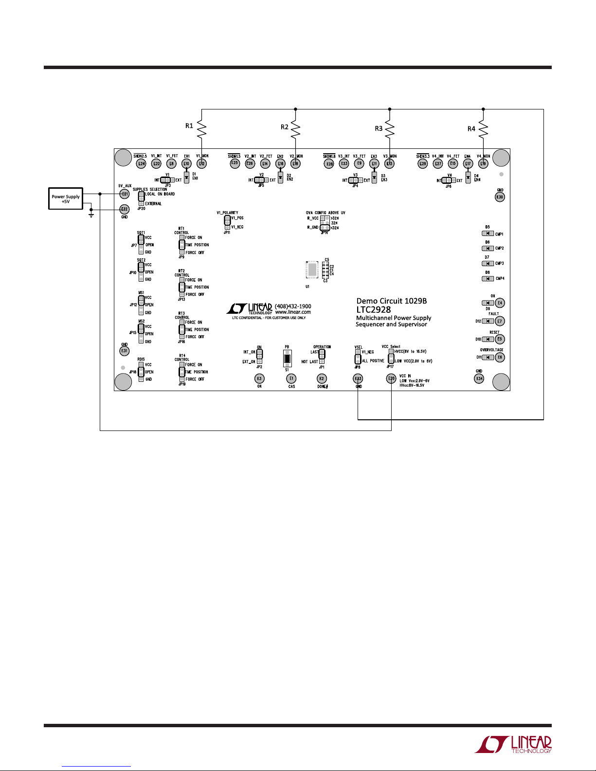
plies. Refer to Figure 1 for the proper circuit connection.
For the load resistors R1, R2, R3, and R4 use 51Ω 1W
resistors. Connect four scope probes to the load resistors
R1, R2, R3, and R4.
Place jumpers in the following positions:
JP1 (OPERATION) LAST
JP2 (ON) INT_ON
JP3 (V1) INT
JP4 (V3) INT
JP5 (V2) INT
JP6 (V4) INT
JP7 (SQT1) GND
JP8 (VSEL) ALL POSITIVE
JP9 (RT1 Control) TIME POSITION
JP10 (SQT2) GND
JP11 (V1 POLARITY) V1_POS
JP12 (MS1) GND
JP13 (RT2 Control) TIME POSITION
JP14 (OVA CONFIG) 32%
JP15 (MS2) GND
JP16 (RT3 Control) TIME POSITION
JP17 (VCC Select) LOW VCC
JP18 (RDIS) OPEN
JP19 (RT4 Control) TIME POSITION
1. With the +5V power supply off, connect the supply to
the 5V_AUX and GND turrets.
2. Turn the +5V supply on and after that switch the ONcon-
trol signal from low to high by pressing the buttonS1.
3. The power-up output voltages should correlate with the
transient shown in Figure 3 (power-up phase). Accept-
able tolerance in the sequence timing is ±20%.
4. Press the button PB (S1) to change the ON signal
from high to low and observe the output voltages. The
power-down output voltages should correlate with the
transient shown in Figure 3. (power-down phase). Ac-
ceptable tolerance in the sequence timing is ±20%.
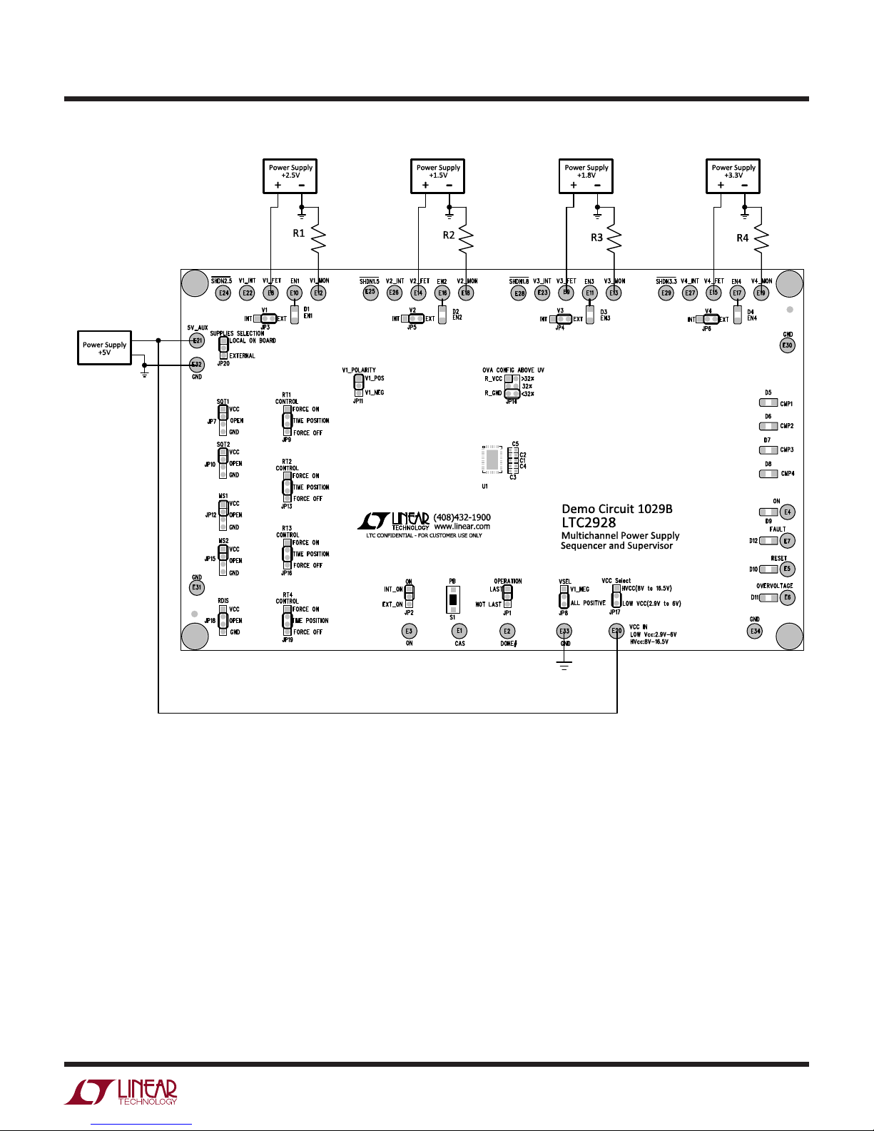
5. Turn the +5V power supply off and connect four ex-
ternal power supply terminals with DC1029 as shown
in Figure 2. Use external power supplies with output
voltages +2.5V, +1.5V, +1.8V, and +3.3V. Leave output
loads as in previous experiments or replace them with
3W resistors 2.5Ω, 1.5Ω, 2Ω, and 3Ω accordingly to
have current in each rail around 1A.
6. Change jumpers V1 (JP1), V2 (JP2), V3 (JP3), and V4
(JP4) positions from INT to EXT.
7. Turn-on all five power supplies. Pushing the button
PB (S1) changes the ON signal from low to high and
after the power-up transient completes, press PB (S1)
a second time to initiate the power-down. The output
voltage sequence timing should be similar to the timing
with the internal power supplies.
8. The DC1029B could be used for the original customer
design. Based on the sequence timing and threshold
parameters define all the optional components’values,
replace them on the board and verify design perfor-
mance. Contact LTC Field Applications Engineers to
get help in the designing or verifying your circuit with
a special tool.
4
dc1029bf
DEMO MANUAL DC1029B
Figure1. Demo Circuit 1029 Connections for Operation with Internal Supplies
QUICK START PROCEDURE
5
dc1029bf
DEMO MANUAL DC1029B
Figure2. Demo Circuit 1029 Connections for Operation with External Supplies
QUICK START PROCEDURE

6
dc1029bf
DEMO MANUAL DC1029B
Figure 3. Power-Up and Power-Down Transients
QUICK START PROCEDURE

7
dc1029bf
DEMO MANUAL DC1029B
5
5
4
4
3
3
2
2
1
1
D D
C C
B B
A A
MS2
RDIS
OVA
EN1
RT2
RT3
RT4
MS1
CMP4
CMP3
V3
EN3
EN4
PTMR
RTMR
STMR
OV#
RT1
SQT1
REF
SQT2
ON
V2
V4
CMP2
EN2
CMP1
FLT#
V1
CAS
RST#
VSEL
EN2
CMP1
EN3
CMP3
CMP4
EN4
CMP2
FLT#
OV#
RST#
REF
EN1
OVA
MS1
RT4
RT1
RT2
SQT2
SQT1
RT3
RDIS
MS2
ON
V2
V1
VSEL
V4
V3
VCC
VCC
HVCC
SIZE
MODIFY DATE:
IC NO. REV.
SHEET OF
TITLE:
APPROVALS
PCB DES.
APP ENG.
TECHNOLOGY
CUSTOMER NOTICE
LINEAR TECHNOLOGY HAS MADE A BEST EFFORT TO DESIGN A
CIRCUIT THAT MEETS CUSTOMER-SUPPLIED SPECIFICATIONS;
HOWEVER, IT REMAINS THE CUSTOMER'S RESPONSIBILITY TO
VERIFY PROPER AND RELIABLE OPERATION IN THE ACTUAL
APPLICATION. COMPONENT SUBSTITUTION AND PRINTED
CIRCUIT BOARD LAYOUT MAY SIGNIFICANTLY AFFECT CIRCUIT
PERFORMANCE OR RELIABILITY. CONTACT LINEAR
TECHNOLOGY APPLICATIONS ENGINEERING FOR ASSISTANCE.
THIS CIRCUIT IS PROPRIETARY TO LINEAR TECHNOLOGY AND
SCHEMATIC
SUPPLIED FOR USE WITH LINEAR TECHNOLOGY PARTS.
SCALE = NONE
www.linear.com
1
15
Vlad Ostrerov
REVISION HISTORY
DESCRIPTION DATE
APPROVED
ECO REV
Vlad Ostrerov
Replaced obsolete LED's
B
Oct 20, 2015
REVISION HISTORY
DESCRIPTION DATE
APPROVED
ECO REV
Vlad Ostrerov
Replaced obsolete LED's
B
Oct 20, 2015
REVISION HISTORY
DESCRIPTION DATE
APPROVED
ECO REV
Vlad Ostrerov
Replaced obsolete LED's
B
Oct 20, 2015
E1
CAS
C3
1uF
25V
C4
1uF
25V
C1 0.022uF
E2
DONE#
C2 2.2uF
U1
LTC2928CUHF
OVA
1
EN1
2
V1
3
NC
4
REF
5
RT1
6
RT2
7
RT3
8
RT4
9
SQT1
10
SQT2
11
MS1
12
MS2
13
RDIS
14
CAS
15
ON
16
NC
17
DONE#
18
FLT#
19
OV# 20
RST# 21
VCC 22
HVCC 23
GND 24
VSEL 25
STMR 26
PTMR 27
RTMR 28
EN4 29
V4 30
EN3 31
V3 32
CMP3 33
CMP4 34
CMP1 35
CMP2 36
EN2 37
V2 38
R1
3.3K
C5
0.047uF
JP1
LAST
NOT LAST
OPERATION
1
3
2
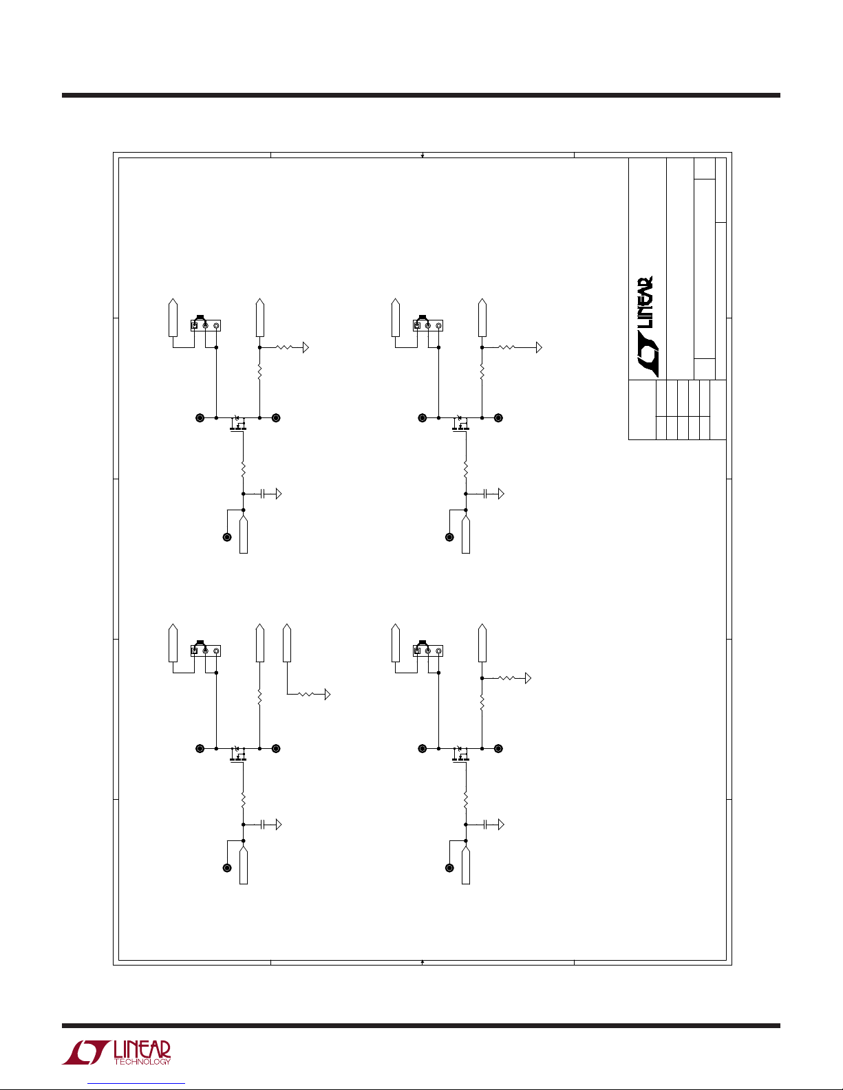
SCHEMATIC DIAGRAM

8
dc1029bf
DEMO MANUAL DC1029B
5
5
4
4
3
3
2
2
1
1
D D
C C
B B
A A
CMP3
ON
FLT#
CMP1
EN4
CMP2
EN3
OV#
RST#
RST# FLT#
EN1
EN4
CMP3
EN1
CMP4
EN2 CMP4
CMP1
ON
OV#
EN2
CMP2
EN3
ON
CMP4
EN1
RST#
CMP3
ON
CMP2
EN4
CMP1
EN2
FLT#
EN3
OV#
5V_AUX
5V_AUX
VCC
5V_AUX
VCC
SIZE
MODIFY DATE:
IC NO. REV.
SHEET OF
TITLE:
APPROVALS
PCB DES.
APP ENG.
TECHNOLOGY
SCHEMATIC
SCALE = NONE
www.linear.com
1
25
Vlad Ostrerov
SIZE
MODIFY DATE:
IC NO. REV.
SHEET OF
TITLE:
APPROVALS
PCB DES.
APP ENG.
TECHNOLOGY
SCHEMATIC
SCALE = NONE
www.linear.com
1
25
Vlad Ostrerov
SIZE
MODIFY DATE:
IC NO. REV.
SHEET OF
TITLE:
APPROVALS
PCB DES.
APP ENG.
TECHNOLOGY
SCHEMATIC
SCALE = NONE
www.linear.com
1
25
Vlad Ostrerov
R39
10K
Q6
2N7002
R2
300
D11
RED
OVERVOLTAGE
R13
1.5K
Q9
2N7002
U2
LTC2950CTS8-1
GND
4
INT 5
PB
2
KILL 8
ONT
3
EN/EN 6
VIN
1
OFFT
7
Q1
2N7002
R9
300
Q7
2N7002
R3
300
D4
YEL
EN4 D6
ORN
CMP2
C6
0.1uF
JP2
INT_ON
EXT_ON
ON
1
3
2
Q4
2N7002
D5
ORN
CMP1
Q2
2N7002 Q5
2N7002
D3
YEL
EN3
E5
RESET
E7
FAULT
E4
ON
R14
1.5K
R8
300
R6
300
R10
10K
Q8
2N7002
D8
ORN
CMP4
R12
1.5K
E3
ON
R7
300
R11
300
D12
RED
FAULT
D2
YEL
EN2
R4
300
R5
300
Q3
2N7002
C7
4700pF
E6
OVERVOLTAGE
S1
PB
C8
4700pF
D10
RED
RESET
D7
ORN
CMP3
D9
GRN
ON
D1
YEL
EN1
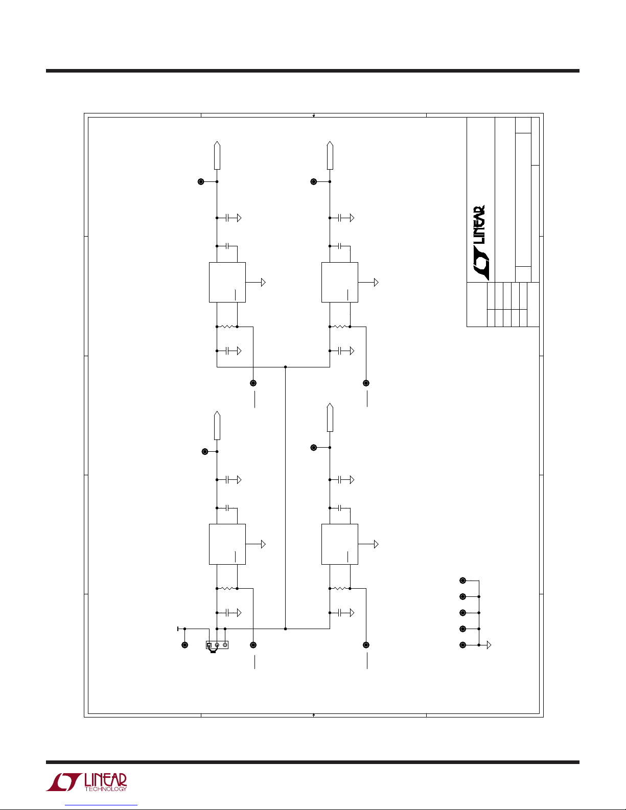
SCHEMATIC DIAGRAM
9
dc1029bf
DEMO MANUAL DC1029B
5
5
4
4
3
3
2
2
1
1
D D
C C
B B
A A
EN2
V2
V1
V4_MON
EN4
V4_FET
V3_FET
V4
EN3
V3_MON
V2_MON
EN1
V1_MON V3
V1_POL
V2_FET
V1_FET
V1
V3
V2_INT
V1_INT
V1_POL
V3_INT
V4
V4_INT
V2
EN2
EN3
EN4
EN1
SIZE
MODIFY DATE:
IC NO. REV.
SHEET OF
TITLE:
APPROVALS
PCB DES.
APP ENG.
TECHNOLOGY
SCHEMATIC
SCALE = NONE
www.linear.com
1
35
Vlad Ostrerov
SIZE
MODIFY DATE:
IC NO. REV.
SHEET OF
TITLE:
APPROVALS
PCB DES.
APP ENG.
TECHNOLOGY
SCHEMATIC
SCALE = NONE
www.linear.com
1
35
Vlad Ostrerov
SIZE
MODIFY DATE:
IC NO. REV.
SHEET OF
TITLE:
APPROVALS
PCB DES.
APP ENG.
TECHNOLOGY
SCHEMATIC
SCALE = NONE
www.linear.com
1
35
Vlad Ostrerov
Q11
IRL3704ZSPBF
R26
49.9K
1%
E19
V4_MON
E15
V4_FET
R18
118K
1%
JP4
INT
EXT
V3
1
3
2
C12
TBD
R19
49.9K
1%
E14
V2_FET
E13
V3_MON
C10
TBD
R21
100
Q10
IRL3704ZSPBF
R22
100
E11
EN3
R17
182K
1%
R15
100
E8
V1_FET
Q12
IRL3704ZSPBF
C11
TBD
R24
261K
1%
JP6
INT
EXT
V4
1
3
2
E17
EN4
E18
V2_MON
Q13
IRL3704ZSPBF
JP5
INT
EXT
V2
1
3
2
R25
49.9K
1%
R23
88.7K
1%
R16
100
JP3
INT
EXT
V1
1
3
2
E10
EN1
E9
V3_FET
E12
V1_MON
R20
49.9K
1%
E16
EN2
C9
TBD
SCHEMATIC DIAGRAM

10
dc1029bf
DEMO MANUAL DC1029B
5
5
4
4
3
3
2
2
1
1
D D
C C
B B
A A
RDIS
VSEL
MS1
SQT1
V1_POL
OVA
REF
SQT2
V1
HVCC
LOW VCC
RT1
RT2
RT3
RT4
MS2
MS2
RT1
SQT1
OVA
V1_POL
RDIS
MS1
SQT2
VSEL
RT2
RT3
RT4
REF
V1
VCC
VCC
VCC
VCC
VCC
VCC
VCC
VCC
VCC
VIN
VCC
VCC
VCC
HVCC
SIZE
MODIFY DATE:
IC NO. REV.
SHEET OF
TITLE:
APPROVALS
PCB DES.
APP ENG.
TECHNOLOGY
SCHEMATIC
SCALE = NONE
www.linear.com
1
45
Vlad Ostrerov
SIZE
MODIFY DATE:
IC NO. REV.
SHEET OF
TITLE:
APPROVALS
PCB DES.
APP ENG.
TECHNOLOGY
SCHEMATIC
SCALE = NONE
www.linear.com
1
45
Vlad Ostrerov
SIZE
MODIFY DATE:
IC NO. REV.
SHEET OF
TITLE:
APPROVALS
PCB DES.
APP ENG.
TECHNOLOGY
SCHEMATIC
SCALE = NONE
www.linear.com
1
45
Vlad Ostrerov
JP7
VCC
GND
SQT1
OPEN
1
3
2
4
JP15
VCC
OPEN
GND
MS2
1
3
2
4
JP19
FORCE ON
TIME POSITION
FORCE OFF
RT4 CONTROL
1
3
2
4
R34
3.40K
1%
R27
95.3K
1%
JP10
VCC
GND
SQT2
OPEN
1
3
2
4
JP13
FORCE ON
TIME POSITION
FORCE OFF
RT2 CONTROL
1
3
2
4
JP11
V1_POS
V1_NEG
V1_POLARITY
1
3
2
JP14
>32%
32%
<32%
OVA CONFIG ABOVE UV
R_VCC
R_GND
1
3
2
4
65
R30
24.3K
1%
R28
TBD
JP18
VCC
OPEN
GND
RDIS
1
3
2
4
R32
9.53K
1%
JP9
FORCE ON
TIME POSITION
FORCE OFF
RT1 CONTROL
1
3
2
4
R29
(Opt)
R33
5.1K
JP8
V1_NEG
ALL POSITIVE
VSEL
1
3
2
E20
VCC IN
LOW Vcc:2.9V-6V
HVcc:8V-16.5V
JP12
VCC
OPEN
GND
MS1
1
3
2
4
JP16
FORCE ON
TIME POSITION
FORCE OFF
RT3 CONTROL
1
3
2
4
R31
(Opt)
JP17
HVCC(8V to 16.5V)
LOW VCC(2.9V to 6V)
VCC Select
1
3
2
SCHEMATIC DIAGRAM
11
dc1029bf
DEMO MANUAL DC1029B
Information furnished by Linear Technology Corporation is believed to be accurate and reliable.
However, no responsibility is assumed for its use. Linear Technology Corporation makes no representa-
tion that the interconnection of its circuits as described herein will not infringe on existing patent rights.
5
5
4
4
3
3
2
2
1
1
D D
C C
B B
A A
V2_INT V4_INT
V1_INT V3_INT V3_INT
V2_INT
V1_INT
V4_INT
5V_AUX
SIZE
MODIFY DATE:
IC NO. REV.
SHEET OF
TITLE:
APPROVALS
PCB DES.
APP ENG.
TECHNOLOGY
SCHEMATIC
SCALE = NONE
www.linear.com
1
55
Vlad Ostrerov
SIZE
MODIFY DATE:
IC NO. REV.
SHEET OF
TITLE:
APPROVALS
PCB DES.
APP ENG.
TECHNOLOGY
SCHEMATIC
SCALE = NONE
www.linear.com
1
55
Vlad Ostrerov
SIZE
MODIFY DATE:
IC NO. REV.
SHEET OF
TITLE:
APPROVALS
PCB DES.
APP ENG.
TECHNOLOGY
SCHEMATIC
SCALE = NONE
www.linear.com
1
55
Vlad Ostrerov
E31
GND
E22
V1_INT
C14
0.01uF
R38
10K
R36
10K
C22
10uF
6.3V
C21
10uF
6.3V
E26
V2_INT
E28
SHDN1.8
C13
10uF
6.3V
U4
LT1761ES5-1.5
IN
1
GND
2
BYP 4
SHDN
3
OUT 5
C23
0.01uF
E27
V4_INT
E30
GND
U5
LT1761ES5-1.8
IN
1
GND
2
BYP 4
SHDN
3
OUT 5
R35
10K
C24
10uF
6.3V
E21
5V_AUX
JP20
SUPPLIES SELECTION
EXTERNAL
LOCAL ON BOARD
1
3
2
C19
10uF
6.3V
C15
10uF
6.3V
E32
GND E34
GND
E29
SHDN3.3
C20
0.01uF
E24
SHDN2.5
C18
10uF
6.3V
C17
0.01uF
E25
SHDN1.5
U6
LT1761ES5-3.3
IN
1
GND
2
BYP 4
SHDN
3
OUT 5
C16
10uF
6.3V
U3
LT1761ES5-2.5
IN
1
GND
2
BYP 4
SHDN
3
OUT 5
E33
GND
E23
V3_INT
R37
10K
SCHEMATIC DIAGRAM

12
dc1029bf
DEMO MANUAL DC1029B
Linear Technology Corporation
1630 McCarthy Blvd., Milpitas, CA 95035-7417
(408) 432-1900 ●FAX: (408) 434-0507 ●www.linear.com
© LINEAR TECHNOLOGY CORPORATION 2015
LT 1215 • PRINTED IN USA
DEMONSTRATION BOARD IMPORTANT NOTICE
Linear Technology Corporation (LTC) provides the enclosed product(s) under the following AS IS conditions:
This demonstration board (DEMO BOARD) kit being sold or provided by Linear Technology is intended for use for ENGINEERING DEVELOPMENT
OR EVALUATION PURPOSES ONLY and is not provided by LTC for commercial use. As such, the DEMO BOARD herein may not be complete
in terms of required design-, marketing-, and/or manufacturing-related protective considerations, including but not limited to product safety
measures typically found in finished commercial goods. As a prototype, this product does not fall within the scope of the European Union
directive on electromagnetic compatibility and therefore may or may not meet the technical requirements of the directive, or other regulations.
If this evaluation kit does not meet the specifications recited in the DEMO BOARD manual the kit may be returned within 30 days from the date
of delivery for a full refund. THE FOREGOING WARRANTY IS THE EXCLUSIVE WARRANTY MADE BY THE SELLER TO BUYER AND IS IN LIEU
OF ALL OTHER WARRANTIES, EXPRESSED, IMPLIED, OR STATUTORY, INCLUDING ANY WARRANTY OF MERCHANTABILITY OR FITNESS
FOR ANY PARTICULAR PURPOSE. EXCEPT TO THE EXTENT OF THIS INDEMNITY, NEITHER PARTY SHALL BE LIABLE TO THE OTHER FOR
ANY INDIRECT, SPECIAL, INCIDENTAL, OR CONSEQUENTIAL DAMAGES.
The user assumes all responsibility and liability for proper and safe handling of the goods. Further, the user releases LTC from all claims
arising from the handling or use of the goods. Due to the open construction of the product, it is the user’s responsibility to take any and all
appropriate precautions with regard to electrostatic discharge. Also be aware that the products herein may not be regulatory compliant or
agency certified (FCC, UL, CE, etc.).
No License is granted under any patent right or other intellectual property whatsoever. LTC assumes no liability for applications assistance,
customer product design, software performance, or infringement of patents or any other intellectual property rights of any kind.
LTC currently services a variety of customers for products around the world, and therefore this transaction is not exclusive.
Please read the DEMO BOARD manual prior to handling the product. Persons handling this product must have electronics training and
observe good laboratory practice standards. Common sense is encouraged.
This notice contains important safety information about temperatures and voltages. For further safety concerns, please contact a LTC application
engineer.
Mailing Address:
Linear Technology
1630 McCarthy Blvd.
Milpitas, CA 95035
Copyright © 2004, Linear Technology Corporation
Table of contents


