LITEMAX ALF/ALH1548 User manual

Page 1
LITEMAX ALF/ALH1548
Sunlight Readable 15” LCD Display
(1st Edition 8/23/07)
All information is subject to change without notice.
LITEMAX Electronics Inc.
8F, No.137, Lane 235, Bau-chiau Rd.,
Shin-dian City, Taipei County, Taiwan R.O.C.
Tel : 886-2-8919-1858
Fax: 886-2-8919-1300
Homepage: http://www.litemax.com.tw

Contents
1.0 HandlingPrecautions.............................................................3
2.0 General Description...............................................................4
2.1DisplayCharacteristics ..............................................................................................................4
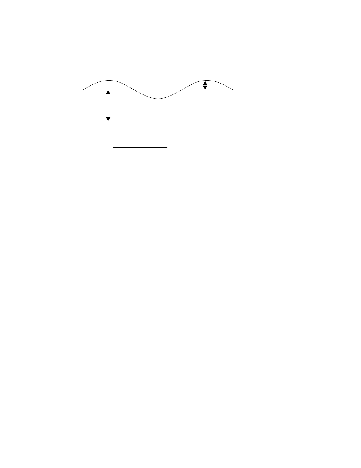
2.2Optical Characteristics
...............................................................................................................5
3.0 Functional Block Diagram....................................................9
4.0 AbsoluteMaximum Ratings.................................................10
4.1TFTLCD Module ......................................................................................................................10
4.2BacklightUnit
............................................................................................................................10
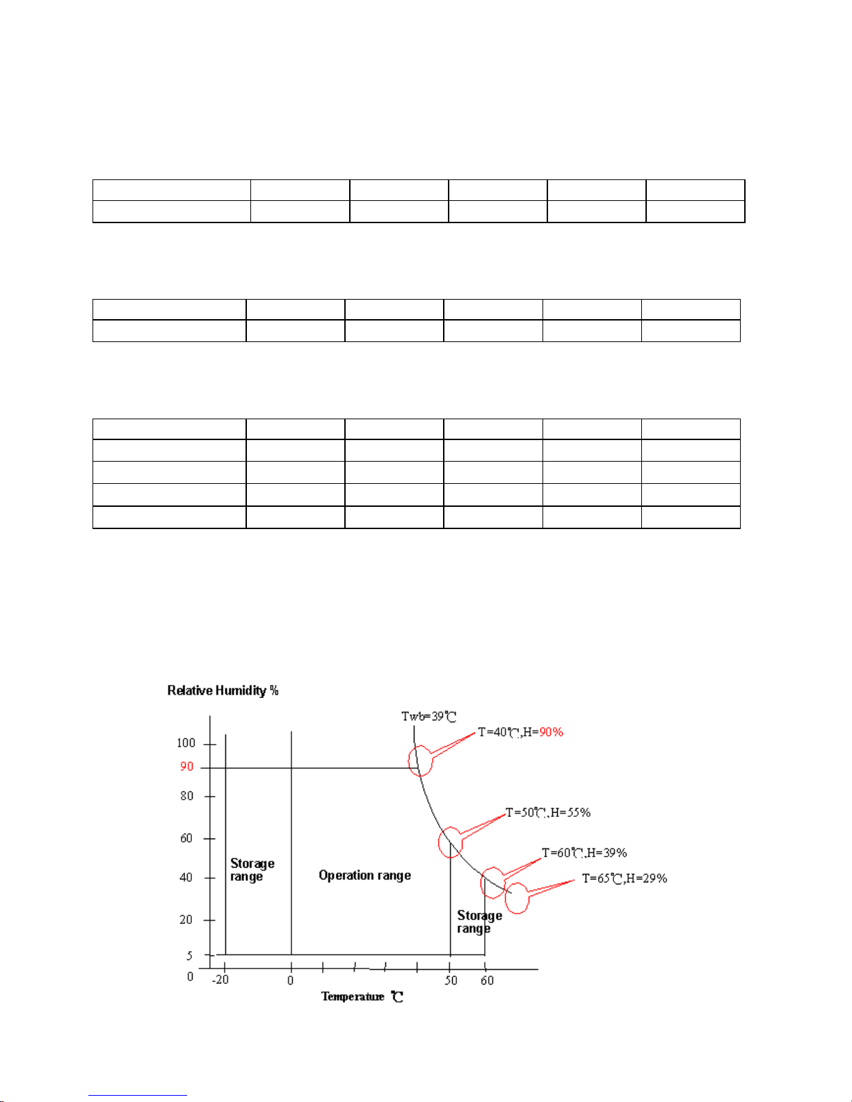
4.3Absolute Ratingsof Environment............................................................................................10
5.0 Electricalcharacteristics......................................................11
5.1TFTLCD Module ......................................................................................................................11
5.1.1 Power Specification.............................................................................................................................11
5.1.2 Signal Electrical Characteristics...........................................................................................................12
5.2BacklightUnit
............................................................................................................................13
6.0 SignalCharacteristic............................................................14
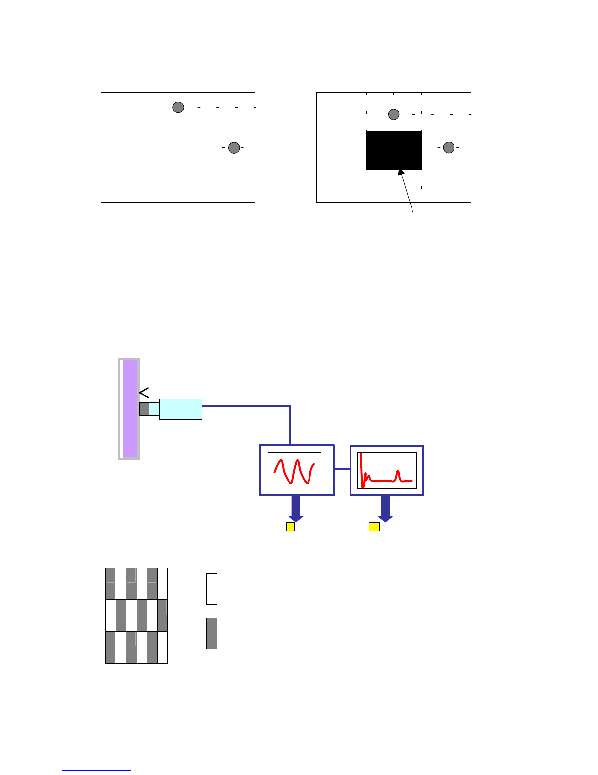
6.1PixelFormat Image...................................................................................................................14
6.2Theinput dataformat ...............................................................................................................15
6.3Signal Description
....................................................................................................................16
6.4InterfaceTiming ........................................................................................................................17
6.4.1 TimingCharacteristics.........................................................................................................................17
6.4.2 Timingdiagram....................................................................................................................................18
6.5Power ON/OFF Sequence
.......................................................................................................19
7.0 Connector & Pin Assignment...............................................20
7.1TFTLCD Module
......................................................................................................................20
7.2BacklightUnit............................................................................................................................21
7.3Signal for Lampconnector.......................................................................................................21
8.0 Reliability............................................................................22
9.0 Safety..................................................................................23
9.1Sharp Edge Requirements ......................................................................................................23
9.2Materials
....................................................................................................................................23
9.2.1 Toxicity................................................................................................................................................23
9.2.2 Flammability........................................................................................................................................23
9.3Capacitors .................................................................................................................................23
10.0Otherrequirement.............................................................23
10.1 National Test Lab Requirement.............................................................................................23
Page 2

1.0 Handling Precautions
1) Since front polarizer iseasilydamaged, payattentionnot toscratchit.
2) Besure to turn off power supplywheninsertingor disconnectingfrom input connector.
3) Wipe offwater dropimmediately.Long contactwith watermaycause discoloration or spots.
4) When the panelsurface issoiled, wipeit withabsorbentcotton or othersoft cloth.
5) Since the panel ismade ofglass,it maybreakor crackifdroppedorbumped onhardsurface.
6) SinceCMOSLSI isusedin thismodule, takecareofstaticelectricityand insure human earth when
handling.
7) Donot open normodifythe Module Assembly.
8) Donot pressorpat the panel surfacebyfingers,handortooling.
9) Donot pressthe reflector sheetatthebackofthemoduleto anydirections.
10)Incase if amodule has tobeputbackintothepacking containerslotafter onceit was takenout fromthe
container, donotpress thecenteroftheCCFL reflector edge.Instead, press at the far endsoftheCCFL
reflector edge softly.Otherwise theTFT module maybe damaged.
11)Atthe insertionor removaloftheSignal InterfaceConnector,besurenot to rotatenortilttheInterface
Connector ofthe TFT module.
12)After installationofthe TFTmodule into anenclosure (DesktopmonitorBezel, forexample),donottwist
nor bend theTFTModuleevenmomentary.Atdesigning theenclosure, it shouldbetakeninto
consideration that nobending/twistingforcesare appliedtotheTFT modulefromoutside.Otherwisethe
TFTmodule maybe damaged.
Page 3

2.0 General Description
Thisspecificationappliestothe 15.0 inchColorTFT/LCD ModuleM150XN07 V2.
Thismodule isdesignedforadisplayunit ofpersonal computer.
ThedisplaysupportstheXGA (1024 (H) x768(V)) screen formatand16.2Mcolors(RGB 6-bits+FRC data).
All inputsignalsare 1 Channel LVDSinterfacecompatible.
Thismodule doesnotcontainan inverter cardfor backlight.
2.1DisplayCharacteristics
Thefollowingitemsare characteristicssummaryon thetable under 25 condition:
ITEMSUnitSPECIFICATIONS
Screen Diagonal [mm]381(15 )
Active Area [mm]304.128(H) x228.096
PixelsH xV1024(x3)x768
Pixel Pitch[mm]0.297 (per one triad)x0.297
Pixel ArrangementR.G.B.Vertical Stripe
DisplayModeTN mode, NormallyWhite
White Luminance[cd/m
2]1600(Typ)@ 5.6mA
Contrast Ratio500:1 (Typ)
OpticalRise Time/FallTime[msec]12 (Typ) (Note 1)
ColorSaturation65%NTSC
Nominal Input Voltage VDD[Volt]+3.3V
PowerConsumption
(VDD line+CCFL +A/D+INV.)
[Watt]
55 W(Typ.) @5.6mA(All BlackPattern)
Weight[Grams]1750 (Typ)
Min. Typ. Max.
Horizatal(H)326.0 326.5 327.0
Vertical(V) 253.0 253.5 254.0
Physical Size[mm]
Depth(D) --19.46
Electrical Interface1 Channel LVDS
SupportColor 16.2Mcolors(RGB 6-bit + FRC data)
TemperatureRange
Operating
Storage(Shipping)
[oC]
[oC]
0to +50
-20 to +60
Surface TreatmentHard-coating (3H),anti-glaretreatment
Note 1 :Systemshould warmupforat least one hour
Page 4

LCD Module
PR-880 /
BM5A /
BM7
Module Driving Equipment
measuring distance
2.2OpticalCharacteristics
The opticalcharacteristicsaremeasured understableconditions at 25 (RoomTemperature):
ItemUnitConditionsMin.Typ. Max. Note
Horizontal(Right)
CR = 10 (Left) TBD 65
65 -
Vertical(Up)
CR = 10 (Down) TBD 65
55
keep total
120(Mayb
e60,60)
Horizontal(Right)
CR =5(Left) TBDTBD
Viewing Angle [degree]
Vertical(Up)
CR =5(Down) TBDTBD
Contrastratio NormalDirectionTBD500 -
Rising Time - TBDTBD
Falling Time -TBDTBD
Response Time
[msec]
Rising +Falling -12
Note1
Redx 0.61 0.64 0.67
Redy 0.30 0.33 0.36
Green x 0.27 0.30 0.33
Green y 0.56 0.59 0.62
Blue x 0.12 0.15 0.18
Color / Chromaticity
Coordinates (CIE)
Blue y 0.07 0.10 0.13
Whitex 0.28 0.31 0.34
Color Coordinates(CIE)
White
Whitey 0.30 0.33 0.36
White Luminance@CCFL
5.6mA(center) [cd/m
2]
1600 -
LuminanceUniformity[%] 7580
Note2
Crosstalk(in 75Hz) [%] 1.21.5 Note3
Flicker dB-20 Note4
Equipment Pattern Generator, PowerSupply,Digital Voltmeter, Luminancemeter (PR 880,BM-5A ,
BM7,CS-1000, CA210, SR_3& EZ Contrast(ELDIM)*)
Aperture 1
∘
with 50cm viewing distance
TestPoint Center(VESA point 9)
Environment <1 lux
*’EZ Contrastisdifferent measurementtool with veryclose viewingdistance.
Page 5

Note 1: Definition of Response time
The outputsignalsofphoto detector aremeasuredwhen theinput signalsare changedfrom “Black to “White
(risingtime),and from “White to “Black (fallingtime),respectively.The response timeisintervalbetweenthe
10% and 90%of amplitudes.
Note 2: Brightness uniformity of these 9pointsisdefinedasbelow
%100
9)-(1Points9inLuminanceMaximum
9)-(1points9inLuminanceMinimum
Uniformity ×=
50 %
90 %
90% 50 %
10 %
10%
100
90
10
0
%
Optical
response
White
Black
White
Tr
F
Tr
R
100
90
10
0
%
Optical
response
White
Black
White
Tr
F
Tr
R
Page 6

Note3: Crosstalkisdefined asbelow:
Unit:percentageofdimensionofdisplayarea
lLA-LA’l /LAx100%=1.5%max., LAandLBare brightness at locationA andB
lLB-LB’l /LBx100%=1.5%max., LA’and LB’arebrightness at location A ’and B’
Note 4: TestPaterm:Subchecker Pattern at 127graylevel
R
G
B
R
G
B
R
G
B
R
G
B
R
G
B
R
G
B
0 graylevel
1/2
1/2
1/6
1/6
A
B
1/2
1/2
1/6
1/6
2/3
1/3
1/3
2/3
A’
B’
184 graylevel 184 graylevel
GrayLevel = L127
GrayLevel = L0
30
A
FFT
0
A
Sub Checker Pattern
CA210
30mm
Page 1

Level
DC
Hz)30Level(atAC
log20(dB)Flicker =
Amplitude
Time
DC
AC
Page 8

3.0 Functional Block Diagram
Thefollowingdiagramshowsthe functional blockofthe 15.0 incheswideColorTFT/LCD Module:
CWY20G –A0G16 / MSB240420JST-BHR-03VS-1
MatingType:HRS DF14-20S-1.25C SM02(8.0)B-BHS-1-TB
12 CCFL
Connector
DC/DC
Converter
LVDS
Receiver
Timing
Controller
Gamma
Correction
TFT-LCD
1024(3)*768
Pixels
X-Driver IC
Y-Driver IC
G1
G768
D1 D3072
Inverter
DCPOWER
AUASIC
RSDS
Transmitter
LVDS
+3.3V
Page 9

4.0 Absolute Maximum Ratings
Absolutemaximum ratings ofthe module isas following:
4.1TFTLCD Module
Item
Symbol
Min
Max
Unit
Conditions
Logic/LCD Drive VDD0.3 +3.6 [Volt] Note 1,2
4.2Backlight Unit
Item
Symbol
Min
Max
Unit
Conditions
CCFL CurrentIRCFL -6 [mA] rmsNote 1,2
4.3Absolute Ratings of Environment
Item
Symbol
Min
Max
Unit
Conditions
OperatingTemperature
TOP 0+50[
o
C] Note 3
Operating HumidityHOP 890[%RH] Note 3
StorageTemperatureTST-20 +60[
o
C] Note 3
StorageHumidityHST890[%RH] Note 3
Note 1: Within Ta (25 )
Note 2: Permanent damageto thedevicemayoccur if exceed maximumvalues
Note 3: Forqualityperfermance, please refer to AUOIIS(Incoming Inspection Standard) .Please referthe
graphbelowforthecorresponding oftemperatureand humidity."
Page10

5.0 Electrical characteristics
5.1TFTLCD Module
5.1.1 Power Specification
Input power specifications are asfollows;
Symbol Parameter Min Typ Max Units
Condition
VDD Logic/LCD Drive
Voltage
3.03.3 3.6[Volt] 10%
IDD VDD current -600700[mA] Vin=3.3V , GrayBar Pattern,
at60Hz
IrushLCDInrush Current
--3[A] Note
PDD VDD Power 2.0
2.3[Watt]
Vin=3.3V , GrayBar Pattern,
at60Hz
VDDrp Allowable
Logic/LCD Drive
RippleVoltage
100[mV]
p-p
Vin=3.3V , All BlackPattern,
at75Hz
Note: Measurementconditions:
+5.0V
+12.0V
SW
VCC
R1
47K
R2
1K
VR1
47K
F1
Q3
AO6402
G
D2S
D1
D5
D6
C1
1uF/16V
Q3
AO6402
G
D2 S
D1
D5
D6
C3
0.01uF/25V
C2
1uF/25V
(High to Low)
Control Signal
(LCD Module Input)
90%
10%
Vinrising time
0
V
3.3
V
470
us
+3.3V
Page 11

5.1.2 Signal Electrical Characteristics
Input signalsshall be lowor Hi-Zstatewhen Vinisoff
It isrecommendedtoreferthespecificationsof SN75LVDS82DGG (Texas Instruments)in detail.
Eachsignal characteristics are asfollows;
Symbol Parameter Min Typ Max Units
Condition
VTH DifferentialInput
High Threshold -- 100 [mV] VICM=1.2V Note
VTL DifferentialInput
LowThreshold -100- -[mV] VICM=1.2V Note
VID Input Differential
Voltage 100400600 [mV] Note
VICM
DifferentialInput
Common Mode
Voltage
1.1 -1.45[V] VTH/VTL = ±100mVNote
Note: LVDS Signal Waveform
VTH
│
VID
│
VTL
VICM
VSS
Page 12

5.2Backlight Unit
Parameter guidelineforCCFLInverter
Symbol Parameter Min. Typ. Max. Unit Condition
IRCFLCCFLoperationrange5.6 6 [mA]
rms
(Ta=25oC)
Note 4
ICFLCCFLInrush current--20[mA]
FCFL CCFLFrequency49 51 53 [KHz] (Ta=25
oC) Note 1
ViCFL
(0oC)
(reference)
CCFLIgnition Voltage
1450 --
[Volt]
rms
(Ta=0oC) Note3
ViCF
(25oC)
(reference)
CCFLIgnition Voltage
1100 --
[Volt]
rms
(Ta=25oC) Note 3
VCFL
CCFLDischarge Voltage
-
570 [Volt]
rms
(Ta=25oC) Note 2
PCFL
CCFLPower consumption
@5.6mA(excluding inverter)
- 3.05[ Watt]
(Ta=25
oC) Note 2
Note1:CCFLfrequency should be carefullydetermined to avoid interference between inverterand TFTLCD.
Note2:Calculatorvalue for reference (IRCFLxVCFLx2=PCFL).
Note3:CCFLinverter should be abletogive output a voltagemore than1450 volt. Lampunitsneed1450 volt
minimumfor ignition.
Note4:CCFLlifetime is40,000hrat6.0mA, it’sdefinedaswhenthe brightness isreduced byhalf. It ’srecommended
notto exceed 6.0mAfor CCFL life time concern and it ’sprohibitedtoexceed6.5mAfor safetyconcern.
Page 13

6.0 Signal Characteristic
6.1Pixel Format Image
Followingfigureshowstherelationship ofthe inputsignalsandLCDpixelformat.
Page 14

6.2Theinput data format
DEVSHS
OG0 OR5OR4OR3OR2OR1OR0
OB0 OG3OG4OG1OG2OB1 OG5
OB5OB3OB4OB2
OR7OB7 OR6OB6 OG7OG6
CLKIN+
RIN0 +/-
CLKIN-
Rsvd
Current Cycle
RIN1 +/-
RIN2 +/-
RIN3 +/-
Note1:Please follow PSWG.
Note2:8-bitin
Note3:R/G/Bdata 7:MSB, R/G/B data 0:LSB
Page 15

6.3Signal Description
The module using a pair ofLVDSreceiver SN75LVDS82(Texas Instruments)orcompatible. LVDSisa differential
signal technologyfor LCD interface and highspeed datatransfer device. Transmitter shallbeSN75LVDS83(negative
edgesampling) or compatible . The firstLVDS port(RxOxxx) transmitsoddpixelswhile the second LVDS
port(RxExxx) transmitseven pixels.
CWY20G-A0D1T(PTWO) orMSB240420 (STM)
Pin No.
SymbolDescription
1VDD Power Supply,3.3V(typical)
2VDD Power Supply,3.3V(typical)
3VSS Ground
4VSS Ground
5Rin0- - LVDSdifferential data input (R0-R5, G0)
6Rin0+ +LVDS differential data input(R0-R5, G0)
7VSS Ground
8Rin1- - LVDSdifferential data input (G1-G5,B0-B1)
9Rin1+ +LVDS differential data input(G1-G5, B0-B1)
10VSS Ground
11Rin2- - LVDSdifferential data input (B2-B5, HS, VS, DE)
12Rin2+ +LVDS differential data input(B2-B5,HS,VS,DE)
13VSS Ground
14ClkIN- - LVDSdifferential clock input
15ClkIN+ +LVDS differential clockinput
16VSS Ground
17Rin3- - LVDSdifferential data input (R6-R7, G6-G7,B6-B7)
18Rin3+ - LVDSdifferential data input (R6-R7, G6-G7,B6-B7)
19VSS Ground
20VSS Ground
Note: Please followPSWG.
Page 16

6.4Interface Timing
6.4.1 TimingCharacteristics
Basically,interface timings described here isnot actualinputtiming ofLCD modulebut outputtiming of
SN75LVDS82DGG (Texas Instruments)orequivalent.
Signal Parameter Symbol MIN TYP MAX Unit
Clock TimingClock frequency clk506581 MHz
Horizontalactive Thd 1024 10241024Tclk
Horizontalblanking Thbl 40320400Tclk
HsyncTiming
Horizontalperiod Th1064 13441424Tck
Vertical active Tvd768768768Th
Vertical blanking Tvbl 83875 Th
VsyncTiming
Vertical period Tv 776806843Th
Note:DE modeonly
Note: Typical valuereferto VESA STANDARD
Page 17

6.4.2 Timingdiagram
Page 18

6.5Power ON/OFFSequence
Vinpower and lamp on/offsequence isas follows. Interface signalsare also shown in the chart. Signalsfrom
anysystem shall be Hi-Z stateorlowlevelwhenVin isoff.
10%
10%
10%
10%
10%
90%
90%
0min.
0min.
1sec
min.
10msmax.
Vin
Lamp
On
Signal
0 V
0 V
0 V
200ms
Page 19

7.0Connector & PinAssignment
Physicalinterface isdescribed asfor the connector on module.
These connectorsare capableof accommodating the followingsignalsand willbe following components.
7.1TFTLCD Module
Connector Name/ Designation InterfaceConnector /Interface card
Manufacturer P-TWOorcompatible
Type Part Number CWY20G –A0G16 / MSB240420
MatingHousingPart Number HRSDF14-20S-1.25C
Pin# Signal Name Pin# Signal Name
1 VDD 2VDD
3 VSS 4VSS
5 Rin0- 6 Rin0+
7 VSS 8Rin1-
9 Rin1+ 10VSS
11 Rin2- 12Rin2+
13 VSS 14 ClkIN-
15 ClkIN+ 16VSS
17 Rin3- 18Rin3+
19 VSS 20VSS
Page 20
Table of contents
Other LITEMAX Monitor manuals

LITEMAX
LITEMAX SLO1941 User manual

LITEMAX
LITEMAX SLO1742 User manual

LITEMAX
LITEMAX SLD1968 V1 User manual

LITEMAX
LITEMAX SSD1505 V2 User manual

LITEMAX
LITEMAX SLD0835 Series User manual

LITEMAX
LITEMAX SSF2825 V2 User manual

LITEMAX
LITEMAX SLD2415 User manual

LITEMAX
LITEMAX SLO0615 User manual

LITEMAX
LITEMAX SSD3823 Spanpixel User manual

LITEMAX
LITEMAX DLF1858-A User manual