Copyright © Matrix Technology Solutions Ltd.4
General information
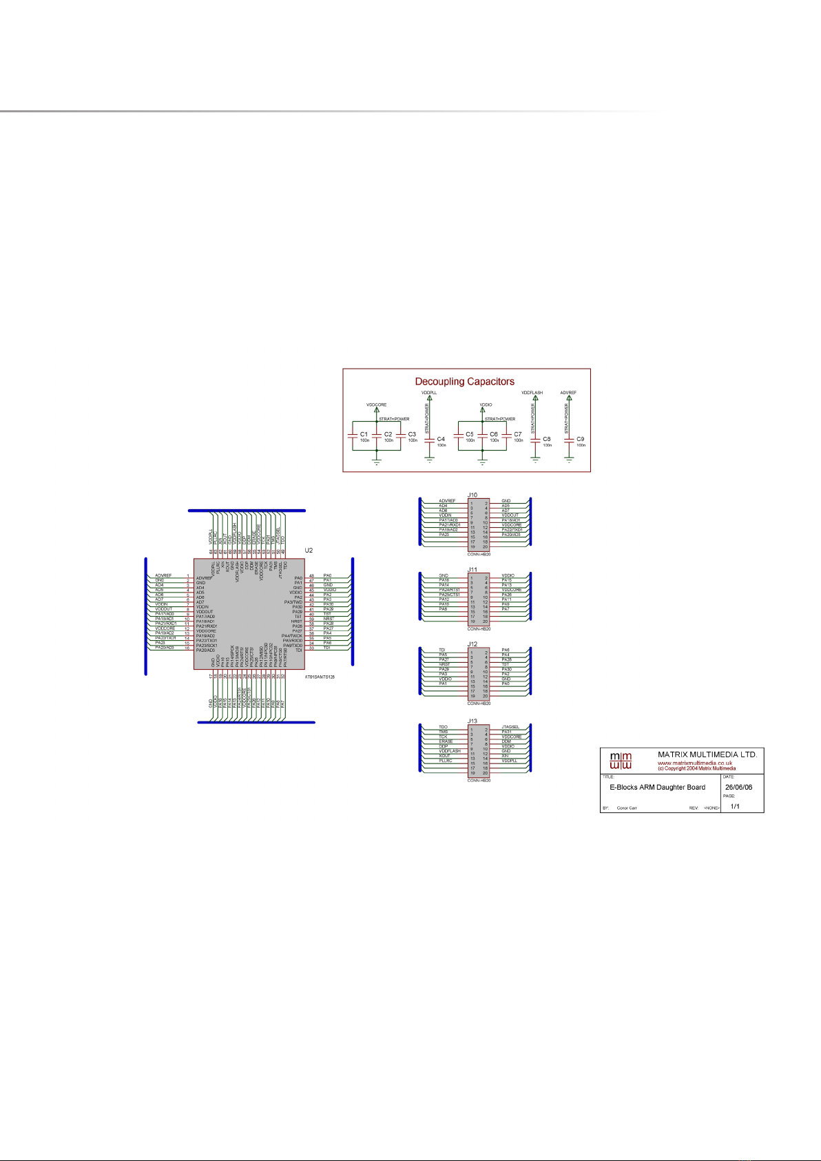
This E-block board is a development tool for the powerful
AT91 SAM 7 microcontroller from Atmel. The SAM 7 is
a 32 bit RISC device running at an interval frequency of
36MHz, and having 128k ROM and 32K static RAM as
well as 2 USARTs, 4 x 10 bit A/D converters and a native
USB bus. This incredibly powerful microcontroller can
be used for a range of advanced E-blocks projects. The
board has ve E-blocks ports and the processor itself
is housed on a removable daughter board (Atmel ARM
processors are only available in SMD technology) so that
the ARM can be incorporated into custom PCBs.
1. Features
• 32 bit RISC processor with 128K ROM and 32K SRAM
• USB programmable with boot loader
• 5 x E-blocks ports, 32 I/O lines
• Compatible with most downstream boards
• Native USB and SPI buses
• Removable crystal
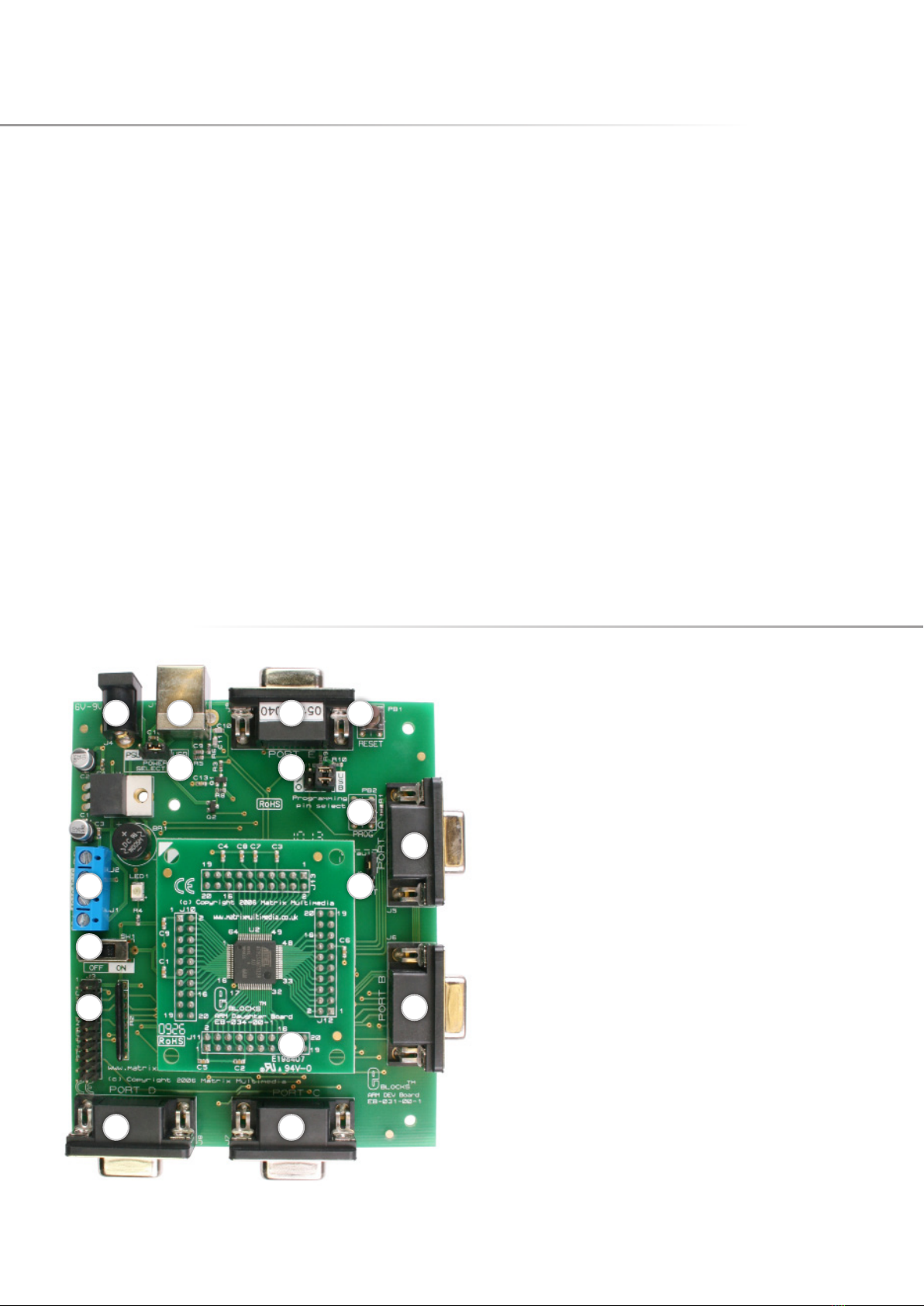
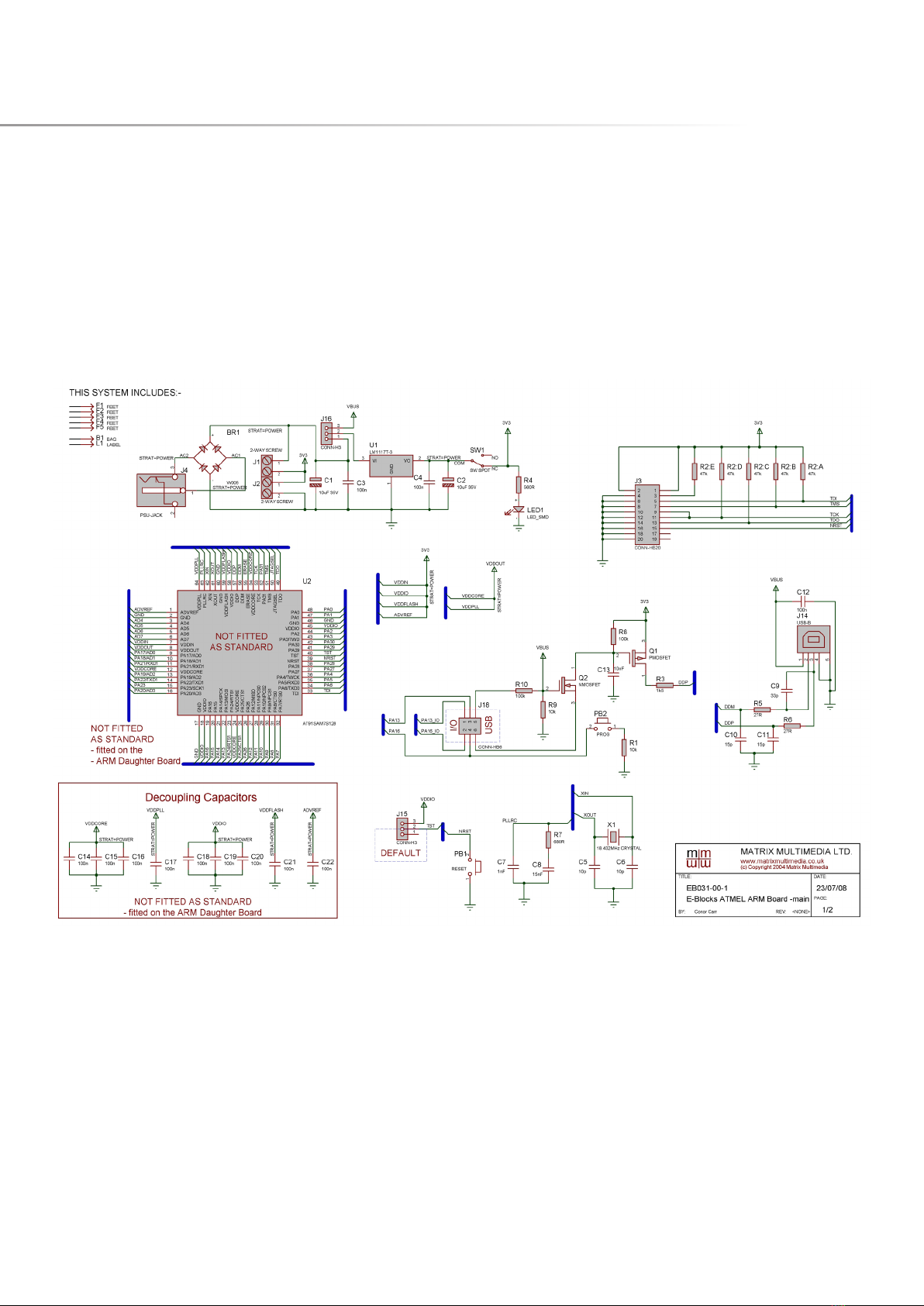
Circuit description
The ARM board solution is made up of two parts:
• A mother board (ARM board EB031) that allows ARM
devices to be programmed and the program to be
executed ‘seamlessly’.
• The ARM daughter board (EB034) that houses the
ARM device on a simple to use board. This allow the
user to program the device using the ARM board
(EB031) and then either use this daughter board in
either the ARM board (EB031) for development, or
to easily use the ARM daughter board in another
project.
1. Power supply
The board is normally operated from an external
regulated DC power supply of 6V - 9V. This allows full
operation including programming.
The board has two modes of power supply; either from
an external regulated DC power supply or powered
using the computer via the USB port. The external
power supply is specied as 6-9V regulated DC power
supply. When using the USB port to power the board,
the user must be aware of the limitations for the use of
this USB port - for example the limited current that can
be supplied via USB (approx. 100mA).
The jumper link system, J16, allows the user to decide
on the source of the power supply. If using an external
power supply the jumper should be positioned to the
left hand side of the jumper system labelled ‘PSU’. If
using USB power place the jumper on the right hand
side of the jumper system. LED1 indicates that power
is supplied to the board from either the external power
supply or the USB cable.
Please note that both USB and the PSU cables should
be removed for the ARM board before changing the
position of this jumper.
Remember that other E-blocks will have to receive 3.3V by
placing a connecting wire from the +V screw terminal of
the ARM board to the +V screw terminal of each E-block
that requires a voltage. Also the user should ensure that
all the E-blocks that they are using are 3.3V compatible.
2. Programming (hardware)
The ARM board connects to a personal computer via
the USC socket. Any USB socket on the PC can be used.
The host ARM device is set-up to communicate with the
USB bus and the programming circuitry. The board uses
MOSFET transistors to detect the USB bus, which allows
the board to be programmed.
The board has a connection (10 +10 DIL PCB header pins)
that allows the ARM device to be programmed via an
external programmer using the JTAG pins available on
the ARM device. This is a standard JTAG connection.
DIL sockets and I/O ports
The ARM board uses an external ARM daughter board.
This daughter board enables the ARM board to be both
a development board and a programmer. This means