Matsushita Electric CQ-C5400W User manual

ORDERNO. ACED040345C3
AUTOMOTIVE AFTERMARKET
CQ-C5400W / CQ-C5300W / CQ-C5100W
RemovableFull Front MP3 WMACD Player / Receiver with CD
Changer Control
SPECIFICATIONS
Specifications*
1

General
Power Supply DC 12V (11V - 16V),
Test Voltage14.4V
NegativeGround
Current Consumption Less than2.2A / (CD mode; 0.5W4
-speaker)
MaximumPower Output 50W×4(at 1kHz)
ToneAdjustment Range Bass : ±12dB at 62Hz
Treble: ±12dB at 16kHz
Equalizer Center Frequency 60Hz, 160Hz, 400Hz, 1kHz, / 3kHz,
6kHz, 16kHz
VariableRangeof Equalizer -12dB to12dB (2dB step)
Speaker Impedance 4-8
Pre-ampOutput Voltage 5V (CD mode; 1kHz, 0dB) / [CQ-
C5400W]
2.5V (CD mode; 1kHz, 0dB) / [CQ-
C5300W/C5100W]
Subwoofer Output Voltage 5V [CQ-C5400W]
2.5V [CQ-C5300W/C5100W]
Pre-ampOutput Impedance 60 [CQ-C5400W]
200 [CQ-C5300W/C5100W]
Subwoofer Output
Impedance 60 [CQ-C5400W]
200 [CQ-C5300W/C5100W]
FM StereoRadio
FrequencyRange 87.5MHz - 108.0MHz
UsableSensitivity 10.2dBf. (0.9 V, 75 )
50dB Quieting Sensitivity 15.2dBf. (1.6 V, 75 )
FrequencyResponse 30Hz-15kHz (±3dB)
AlternateChannel Selectivity75dB
StereoSeparation 35dB (1kHz)
ImageResponse Ratio 75dB
IFResponse Ratio 100dB
Signal toNoise Ratio 62dB
AM Radio
FrequencyRange 531 - 1602kHz
UsableSensitivity 28dB/ V (11 V, S/N 20dB)
CD Player
Sampling Frequency 8 times Oversampling
DAConverter 4 DAC System
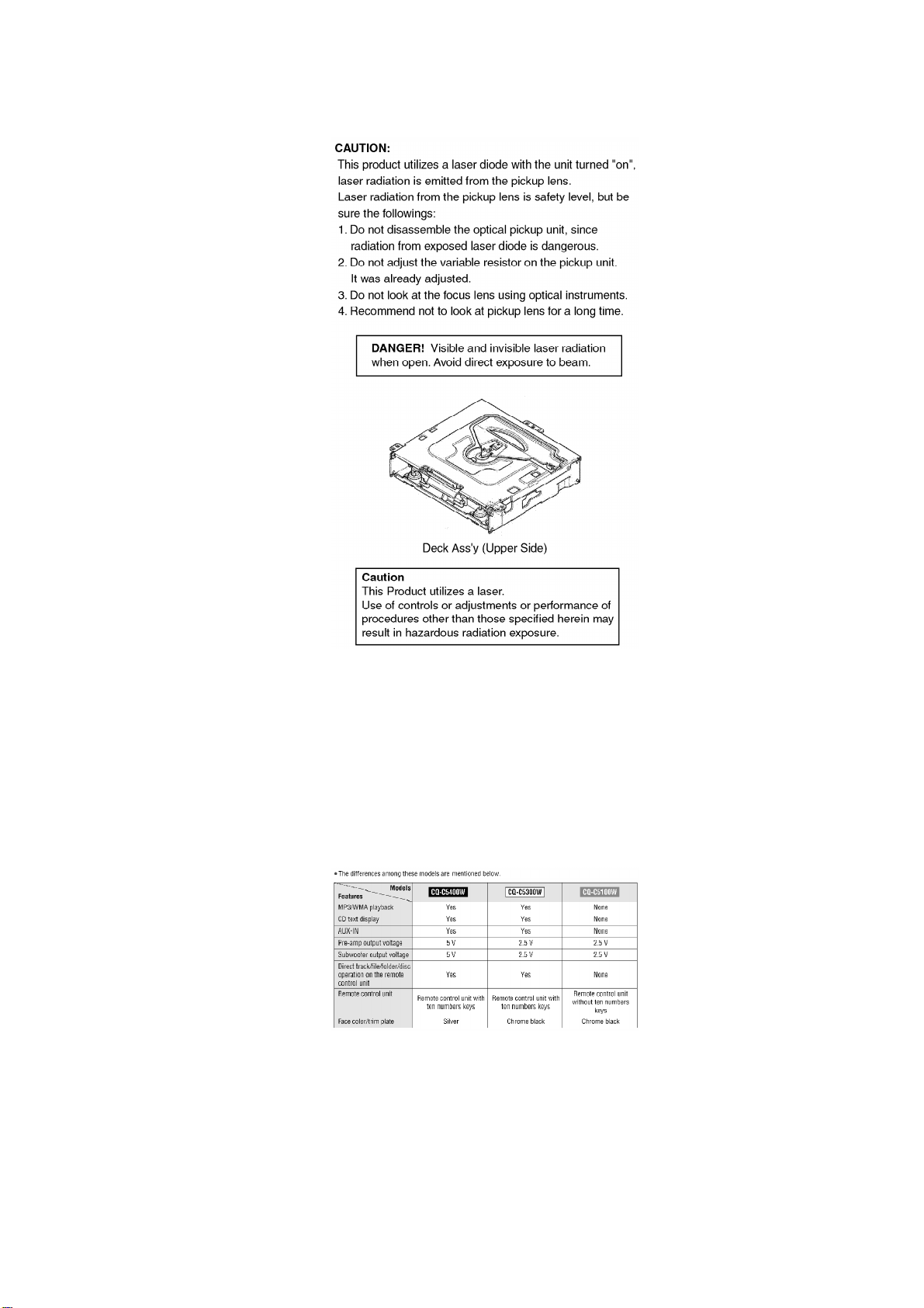
Pick-UpType Astigma 3-beam
Light Source SemiconductorLaser
WaveLength 780nm
FrequencyResponse 20Hz - 20kHz (±1dB)
Signal toNoise Ratio 96dB
Total HarmonicDistortion 0.01%(1kHz)
Wowand Flutter Belowmeasurablelimits
2

Channel Separation 75dB
Dimensions** (W×H×D) 178mm×50mm×155mm
Weight** 1.6kg
*Specificationsand thedesign are subject topossible
modification without notice duetoimprovements.
** Dimensionsand Weight shownare approximate.
-Abovespecificationscomplywith EIAstandards.
2004 Matsushita ElectricIndustrial Co., Ltd. All rights reserved.
Unauthorized copying and distribution isaviolation of law.
3

1. ABOUT LEAD FREE SOLDER (PbF)
Distinction of PbF PCB:
PCBs (manufactured) using leadfree solderwill have a PbF stampon the PCB.
Caution :
-Pb free solder has ahigher melting point than standard solder;
Typicallythe melting point is50 -70°F (30 -40°C)higher. Please
use asoldering iron with temperature control and adjust itto 700 ±
20°F (370 ± 10°C). Incase of using high temperature soldering
iron, please be careful not to heat too long.
-Pb free solder will tend to splash when heated too high (about
1100°F/600°C)
-Thislead free solder will be used for the products after serial No.
1,000,001.
2. LASER PRODUCTS
4

3. FEATUERS
-Digital servo for reliableplayback.
-PLL (Phase Locked Loop) synthesized tuning.
-18-FM, 6-AMpresets with preset scan.
-CD Changer Control
-Removableface plate.
-MP3/WMAPlayback from CD-R/RW. / (CQ-C5400W/CQ-C5300W)
4. REPLACING THE FUSE
Use fuses of the same specifiedrating (15amps). Using different substitutes orfuses with
higherratings, orconnecting the product directlywithout a fuse, couldcause fire ordamage to
the stereounit.
5

5. MAINTENANCE
Yourproduct is designedand manufacturedtoensure a minimumof maintenance. Use a dry, a
soft clothforroutine exteriorcleaning. Neveruse benzine, thinnerorothersolvents.
6. NOTES
[RADIO BLOCK]
Donot align the AM/FM package block. Whenthe package block is necessary, it will be supplied
alreadyalignedat the factory.
[CD DECK BLOCK]
This model has no servoalignment points because microcomputercontrols the servocircuit.
7. DIMENSIONS
8. WIRING CONNECTION
8.1. CQ-C5400W/C5300W
6

8.2. CQ-C5100W
7

9. DISASSEMBLY INSTRUCTIONS
8

10. TERMINALS DESCRIPTION
10.1. MainBlock
IC601 : YESAM238 [CQ-C5400W / CQ-C5300W]
9

Pin
No. Port Description I/O Volt (V)
FM AM CD
1PANEL
OPEN PANELOPEN
detection I5.2 5.2 5.2
2PANEL
CLOSE PANELCLOSE
detection I 0 0 0
3NC NoConnection - - - -
4BATT BATT detection I 5.1 5.1 5.1
5 ACC ACC detection I 5.1 5 5.1
6 SDA Electronic VOLdata I/O 5 5 5
7 SCK Electronic VOLclock O 5 0 5
8 NC NoConnection - - - -
9Vss GND - 0 0 0
10 ST FM STdetection I 5.1 5.1 5.1
11 PLL
DI
(MO)
PLL data output O 0 0 0
12 PLL
DO
(MI)
PLL data input I 5.2 5.2 5.2
13 PLL
CLK PLL clock output O 5 5 5
14 PLL
CE PLL chipenable
output O 0 0 5
15 CD
RST CD deck reset output O 5 5 0
16 SUB SI SUB CPU Data O 4.9 4.9 4.9
17 LCD
CLK LCD clock O 4.8 4.8 4.8
18 SUB
SO SUB CPU Data I 4.2 4.2 4.2
19 CD
SO
(MI)
CD Data I 1.4 1.4 1.4
20 CD
SCK CD clock transmit O 4.9 4.9 4.9
21 Vdd Powersupply I 5 5 5
22 CD SI
(MO) CD Data O 0 0 0
23 NC NoConnection - - - -
24 CDC
CLK CD Changerclock I 0 0 0
25 CONDENSOR
Capacitorforpower
supply - 3.2 3.2 3.2
26 CDC
DATA CD Changerdata I 0 0 0
10

Pin
No. Port Description I/O Volt (V)
FM AM CD
27 CDC
STB Changerstorobe
signal input I 0 0 0
28 CD IN DISC Indetection I 4.9 4.9 0.4
29 DECK
V
CONT
DECK powersupply
control output O 5 5 5
30 CD
STB Strobe signal forCD
communication O3.3 3.3 3.3
31 NC NoConnection - - - -
32 Avdd Powersupplyof D/A
converter I 5.1 5.1 5.1
33 AVREF Reference voltage for
D/A converter I 5.1 5.1 5.1
34 AVGNDReference GND forD/
A converter I 0 0 0
35 AVSS GND forA/D and D/A
converter I 0 0 0
36 SD FM/AM signal
strength I 0.3 0 0.3
37 INITA Initializ A I 0 0 0
38 INITB Initializ B I 0 0 0
39 A IN SPE.ANA A.IN I 0 0 0
40 Vss GND I 0 0 0
41 CD A0 Signal output
according to
command
employment
O 0 0 5.1
42 CD
RFOK
(NC)
NoConnection - - - -
43 CD
LOCK
(NC)
NoConnection - - - -
44 CD
LIMIT
(NC)
NoConnection - - - -
45 CD
SW1
(NC)
NoConnection - - - -
46 CD
SW2
(NC)
NoConnection - - - -
47 MOD0 Operating mode input
0I 5.2 5.2 5.2
48 MOD1 Operating mode input
1I 5.1 5.1 5.1
11

1
12

Pin
No. Port Description I/O Volt (V)
FM AM CD
49 MOD2 Operating mode input
2I 0 0 0
50 H
STANDBY
External standby
input I5.1 5.1 5.1
51 DC
DC
CNT
(NC)
Noconnection - - - -
52 FP
MOTOR1
Front open/close
control 1 O 5 5 5
53 FP
MOTOR2
Front open/close
control 2 O 5 5 5
54 V
CNT1 Panel driving voltage
control 1 O 0 0 0
55 V
CNT2
(NC)
NoConnection - - - -
56 SA
CLK Spectrumanalizer
clock O 5 4.9 4.9
57 EXT
MUTE TEL/NAVI MUTE input I 5.4 5.4 5.4
58 AMP
CONT External AMP control O 5 5 5
59 BZ-
OUT Buzzeroutput O 0 0 0
60 ANT
CONT Motorantenna control O 5 5 0
61 DIM1 Dimmercontrol
output 1 O 0 0 0
62 DIM2 Dimmercontrol
output 2 O 0 0 0
63 CDC
REM
OUT
Remote control data
forCD Changer O 5 5 5
64 CDC
SENS CDC 1/2 detection I 5.1 5.1 5.1
65 CDC 1/
2CDC 1/2 change
output O 0 0 0
66 NC NoConnection - - - -
67 MAIN
W.U
REQ
Mainwake-up request I 4.9 4.9 4.9
68 NC NoConnection - - - -
69 NC NoConnection - - - -
70 NC NoConnection - - - -
71 NC NoConnection - - - -
13

71
NC
No
Connection
-
-
-
-
Pin
No. Port Description I/O Volt (V)
FM AM CD
72 MAIN
CONT MAIN powersupply
control O 5 4.9 4.9
73 INV
CONT INV powersupply
control O5.1 5 5
74 AF
MUTE AFMUTE control O 5.1 5.1 5.1
75 RESET Reset input I 5.1 5.1 5.1
76 NC NoConnection - - - -
77 NC NoConnection - - - -
78 NC - I 0 0 0
79 Vss GND I 0 0 0
80 X1 Crystal oscillator
input I2.1 2.1 2.1
81 X2 Crystal oscillator
output O2.5 2.5 2.5
82 Vdd Powersupply I 5.1 5.1 5.1
83 P00 Pldaun port for
writing I 0 0 0
84 P01 Pull-up port for
writing I5.1 5.1 5.1
85 OFFSET
DET PWR-IC offset
detection I 0 0 0
86 STBY PWR-IC STBY control
output O5.1 5.1 5.1
87 AMP
MUTE PWR-IC MUTE
control output O 0 0 0
88 ILL
SENS External dimmer
control input I5.1 5.1 5.1
89 SUBM
CNT
(NC)
NoConnection - - - -
90 EP DO
(MI) (Ground pull down) - - - -
91 EP D0
(M0)
(NC)
NoConnection - - - -
92 EP SK
(NC) NoConnection - - - -
93 SUB
W U
REQ/
LCD
CE
Sub Wake-up request O 0 0 0
94 DISPM
CNT Powersupplycontrol
fordisplay O 0 0 0
14

Pin
No. Port Description I/O Volt (V)
FM AM CD
95 EJE
ILL
(NC)
NoConnection - - - -
96 Rotary
1RotaryEncoder1 I 4.9 5 5
97 Rotary
2RotaryEncoder2 I 4.9 4.9 5
98 S LED SecurityLED control
output O 0 0 0
99 PANEL
IN PANELdetect I 5.3 5.3 5.3
100 EP CS
(NC) NoConnection - - - -
IC601 : YESAM239 [CQ-C5100W]
Pin
No. Port Description I/O Volt (V)
FM AM CD
1 PANEL
OPEN PANELOPEN
detection I5.2 5.2 5.2
2 PANEL
CLOSE PANELCLOSE
detection I 0 0 0
3NC NoConnection - - - -
4BATT BATT detection I 5.1 5.1 5.1
5 ACC ACC detection I 5.1 5 5.1
6 SDA Electronic VOLdata O 5 5 5
7 SCK Electronic VOLclock O 5 0 5
8 NC NoConnection - - - -
9Vss GND - 0 0 0
10 ST FM STdetection I 5.1 5.1 5.1
11 PLL DI
(MO) PLL data output O 0 0 0
12 PLL
DO (MI) PLL data input I 5.2 5.2 5.2
13 PLL
CLK PLL clock output O 5 5 5
14 PLL CE PLL chipenable
output O 0 0 5
15 CD
RST CD deck reset output O 5 5 0
16 SUB SI SUB CPU Data O 4.9 4.9 4.9
17 LCD
CLK
18 SUB
SO SUB CPU data I 4.2 4.2 4.2
15

Pin
No. Port Description I/O Volt (V)
FM AM CD
19 CD SO
(MI) CD Data recept I 1.4 1.4 1.4
20 CD
SCK CD clock O 4.9 4.9 4.9
21 Vdd Powersupply - 5 5 5
22 CD SI
(MO) CD Data transmit O 0 0 0
23 NC NoConnection - - - -
24 CDC
CLK CD ChangerClock I 0 0 0
25 CONDENSOR
Capacitorforpower
supply - 3.2 3.2 3.2
26 CDC
DATA CD Changerdata I 0 0 0
27 CDC
STB Changerstrobe
signal input I 0 0 0
28 CD IN DISC Indetection I 4.9 4.9 0.4
29 DECK
V
CONT
DECK powersupply
control output O 5 5 5
30 CD
STB Strobe signal forCD
communication O3.3 3.3 3.3
31 CD
OSCSTPCD OSC stop signal
output O - - -
32 Avdd PowersupplyforD/A
converter - 5.1 5.1 5.1
33 AVREF Reference voltage for
D/A converter - 5.1 5.1 5.1
34 AVGND Reference GND forD/
A converter - 0 0 0
35 AVSS GND forA/D and D/A
converter - 0 0 0
36 SD FM/AM signal strength I 0.3 0 0.3
37 INITA Initializ A I 0 0 0
38 INITB Initializ B I 0 0 0
39 A IN SPE.ANA A.IN I 0 0 0
40 Vss GND - 0 0 0
41 CD A0 Signal output
according to
command
employment
O 0 0 5.1
42 CD
RFOK RFOK signal I 5 5 5
43 CD
LOCK CD Lock I 5 5 5
16

Pin
No. Port Description I/O Volt (V)
FM AM CD
44 CD
LIMIT Limit switchsignal I 0 0 0
45 CD
SW1 CD Switch1 I 0 0 0
46 CD
SW2 CD Switch2 I 0 0 0
47 MOD0 Operating mode input
0I 5.2 5.2 5.2
48 MOD1 Operating mode input
1I 5.1 5.1 5.1
49 MOD2 Operating mode input
2I 0 0 0
50 H
STANDBY
External standbyinput I 5.1 5.1 5.1
51 DC DC
CNT
(NC)
NoConnection - - - -
52 FP
MOTOR1
Front open/close
control 1 O 5 5 5
53 FP
MOTOR2
Front open/close
control 2 O 5 5 5
54 V CNT1 Panel driving voltage
control 1 O 0 0 0
55 V
CNT2
(NC)
NoConnection - - - -
56 SA
CLK Spectrumanalizer
clock O 5 4.9 4.9
57 EXT
MUTE TEL/NAVI MUTE input I 5.4 5.4 5.4
58 AMP
CONT External AMP control O 5 5 5
59 BZ-
OUT Buzzeroutput O 0 0 0
60 ANT
CONT Motorantenna control O 5 5 0
61 DIM1 Dimmercontrol
output 1 O 0 0 0
62 DIM2 Dimmercontrol
output 2 O 0 0 0
63 CDC
REM
OUT
Remote Control data
forCD Changer O 5 5 5
64 CDC
SENS CDC 1/2 detection I 5.1 5.1 5.1
17

Pin
No. Port Description I/O Volt (V)
FM AM CD
65 CDC 1/
2CDC 1/2 change
output O 0 0 0
66 NC NoConnection - - - -
67 MAIN.W.U.REQ
Mainwake-up request I 4.9 4.9 4.9
68 RDS
(NC) NoConnection - - - -
69 RDS
CLK
(NC)
NoConnection - - - -
70 NC NoConnection - - - -
71 NC NoConnection - - - -
72 MAIN
CONT MAIN powersupply
control O 5 4.9 4.9
73 INV
CONT INV powersupply
control O5.1 5 5
74 AF
MUTE AFMUTE control O 5.1 5.1 5.1
75 RESET Reset input I 5.1 5.1 5.1
76 NC NoConnection - - - -
77 NC NoConnection - - - -
78 NC NoConnection - - - -
79 Vss GND I 0 0 0
80 X1 Crystal oscillator
input I2.1 2.1 2.1
81 X2 Crystal oscillator
output O2.5 2.5 2.5
82 Vdd Powersupply I 5.1 5.1 5.1
83 P00 Pldaun port forwriting I 0 0 0
84 P01 Pull-up port for
writing I5.1 5.1 5.1
85 OFFSET
DET PWR-IC OFFSET
detection I 0 0 0
86 STBY PWR-IC STBY control
output O5.1 5.1 5.1
87 AMP
MUTE PWR-IC MUTE control
output O 0 0 0
88 ILL
SENS External dimmer
control input I5.1 5.1 5.1
89 SUBM
CONT
(NC)
NoConnection - - - -
90 EP DO
(MI) (Ground pull down) - - - -
18

Pin
No. Port Description I/O Volt (V)
FM AM CD
91 NC/EP
DI
(MO)
(NC)
NoConnection - - - -
92 NC/EP-
SK NoConnection - - - -
93 SUB W
U REQ Sub wake-up request O 0 0 0
94 DISPM
CONT Powersupplycontrol
fordisplay O 0 0 0
95 EJE
ILL(NC) NoConnection - 0 0 0
96 NC/
ROTARY1
RotaryEncoder1 I 4.9 5 5
97 NC/
ROTARY2
RotaryEncoder2 I 4.9 4.9 5
98 S LED SecurityLED control
output O 0 0 0
99 PANEL
IN PANELdetect I 5.3 5.3 5.3
100EP CS
(NC) NoConnection - - - -
10.2. DisplayBlock
IC901 : YESAM168
Pin
No. Port Description I/O (V)
1-51 S3-53 LCD segment data O 2.5
52-
55 COM1-4 LCD common O 2.5
56,
57 KS54, 55 LCD segment data O 2.5
58-
61 KS3-6 Keystrobe O 5.0
62-
66 Kl1-5 Keydata I 0
67 VDD +5V powersupply - 5.0
68 VLCD0 VLCD0 filterterminal - 5.0
69 VLCD1 VLCD1 filterterminal - 3.3
70 VLCD2 VLCD2 filterterminal - 1.7
71 VSS Ground - 0
72 TEST (Connecting toground) - 0
73 OSC Oscillatorterminal - 5.0
19

74 RESET (Connecting to+5V) I 5.0
75 DO Keydata output O 5.0
76 CE LCD driverchipenable I 0
77 CLK LCD clock I 5.0
78 DI LCD data I 5.0
79,
80 S1-2 LCD segment data O 2.5
10.3. CD Servo Block / [CQ-C5400W/CQ-C5300W]
IC401 : YESAM176
Pin
No. Port Descriptions I/O (V)
1 CVSS1 GND - 0
2 - - - -
3 CVSS2 GND - 0
4 DVSS1 I/O system(3.3V) power
supply - 3.3
5 A10 Address bus of FLASH
ROM O 0
6 - - - -
7 A11 Address bus of FLASH
ROM O 3.3
8 A12 O 3.3
9 A13 O 3.3
10 A14 O 3.3
11 A15 O 3.3
12 /CVDD1 CORE CPU system(1.6V)
powersupply - 1.6
13 - - - -
14 DVSS1 GND - 0
15 CVSS3 GND - 0
16 /CVDD2 I/O system(3.3V) power
supply - 1.6
17 - - - -
18 - - - -
19 - - - -
20 nPS FLASH ROM selection
signal O 3.3
21 - - - -
22 - - - -
23 R/W Lead/light signal to
FLASH ROM O 3.3
24 nMSTRBMemoryaccess signal O 3.3
25 - - - -
26 - - - -
20
This manual suits for next models
2
Table of contents
Other Matsushita Electric CD Player manuals