Matsushita Electric CQ-C5403W User manual

ORDER NO.ACED060109C3
AUTOMOTIVE AFTERMARKET
CQ-C5403W / CQ-C5303W
WMA MP3 CD Player/Receiver
SPECIFICATIONS
Specifications*
General
Power Supply DC 12V (11V - 16V),
Test Voltage 14.4V
Negative Ground
Current Consumption Less than 2.1A (CD mode ; 0.5W
4-channels)
Maximum Power Output 50W×4 (at 1kHz)
Volume control Maximum
Power Output 18W×4CH (1kHz, 1%, 4 )
Tone/SQ Adjustment Range SQ Low/Bass ; ±12dB / (at 60Hz,
80Hz, 100Hz, 200Hz)
SQ Mid ; ±12dB / (at 500Hz,
1kHz, 2kHz, 3kHz)
SQ High/Treble ; ±12dB / (at
10kHz, 12kHz, 15kHz, 18kHz)
Speaker Impedance 4-8
Pre-Amp Output Voltage 4V (CD mode; 1kHz, 0dB)
[CQ-C5403W]
2.5V (CD mode ; 1kHz 0dB)
[CQ-C5303W]
Pre-Amp Output Impedance 60 [CQ-C5403W]
200 [CQ-C5303W]
Subwoofer Output Voltage 4V [CQ-C5403W]
2.5V [CQ-C5303W]
1

Subwoofer Output Impedance 60 [CQ-C5403W]
200 [CQ-C5303W]
FM Stereo Radio
Frequency Range 87.5MHz - 108MHz
Usable Sensitivity 6dB/ V (S/N 30dB)
Frequency Response 30Hz-15kHz (±3dB)
Alternate Channel Selectivity 75dB
Stereo Separation 35dB (1kHz)
Image Rejection Ratio 70dB
IF Rejection Ratio 100dB
Signal to Noise Ratio 62dB
AM Radio
Frequency Range 531kHz - 1,602kHz
Usable Sensitivity 28dB/ V (S/N 20dB)
CD Player
Sampling Frequency 8 Times Oversampling
DA Converter 1bit DAC System
Pick-Up Type Astigma 3-beam
Light Source Semiconductor Laser
Wave Length 790nm
Frequency Response 20Hz to 20kHz (±1dB)
Signal to Noise Ratio 96dB
Total Harmonic Distortion 0.01% (1kHz)
Wow and Flutter Below measurable limits
Channel Separation 75dB
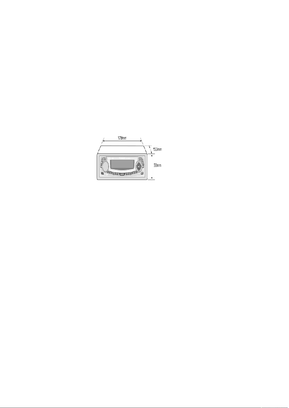
Dimensions** 178×50×155mm
Weight** 1.6kg
* Specifications and the design are subject to possible
modification without notice due to improvements.
** Dimensions and Weight shown are approximate.
-Above specifications comply with EIA standards.
2006 Matsushita Electric Industrial Co., Ltd. All rights reserved.
Unauthorized copying and distribution is a violation of law.
2

1. ABOUT LEAD FREE SOLDER (PbF)
Distinction of PbF PCB:
PCBs (manufactured) using lead free solder will have a PbF stamp on the PCB.
Caution :
- Pb free solder has a higher melting point than standard solder; Typically
the melting point is 50 - 70°F (30 - 40°C) higher. Please use a soldering
iron with temperature control and adjust it to 700 ± 20°F (370 ± 10°C). In
case of using high temperature soldering iron, please be careful not to
heat too long.
- Pb free solder will tend to splash when heated too high (about 1100°F/
600°C)
- This lead free solder will be used for the products after serial No.
1,000,001.
2. LASER PRODUCTS
3

3. FEATUERS
- The optional adapter allows you to connect the optional Panasonic CD
changer unit (CX-DP880).
- The optional adapter allows you to connect the optional iPod series.
- Hands Free Phone System. (The optional Bluetooth hands-free kit: CY-
BT100N)
- Fully Motorized Face Plate.
- SQ (Sound Quality).
- SQ3 (3-Band Sound Quality).
- SRS TruBass (CQ-C5403W).
- This manual is for 2 models CQ-C5403W and CQ-C5303W. The following
table describes the differences between 2 models.
4. REPLACING THE FUSE
4

Use fuses of the same specified rating (15amps). Using different substitutes or fuses with higher
ratings, or connecting the product directly without a fuse, could cause fire or damage to the stereo unit.
5. MAINTENANCE
Your product is designed and manufactured to ensure a minimum of maintenance. Use a dry, a soft
cloth for routine exterior cleaning. Never use benzine, thinner or other solvents.
6. NOTES
[RADIO BLOCK]
Do not align the AM/FM package block. When the package block is necessary, it will be supplied already
aligned at the factory.
[CD DECK BLOCK]
This model has no servo alignment points because microcomputer controls the servo circuit.
7. DIMENSIONS
8. WIRING CONNECTION
5

9. DISASSEMBLY INSTRUCTIONS
9.1. How to remove the Flexible PCB
6

9.2. How to install the Main P.C.B of the Electric Slide Display
10. TERMINALS DESCRIPTION
10.1. Main Block
IC601 : YESAM335
7

Pin
No.
Port Description I/O (V)
FM AM CD
1 BATT
DET
Battery voltage
detection
I 1.9 1.9 1.9
2 AMP
MUTE
Amp mute control O 4.8 4.8 4.8
3 STBY Power IC stundby
control
O 4.8 4.8 4.8
4 FP
MOTOR1
Panel motor
control 1
O 4.7 4.7 4.7
5 FP
MOTOR2
Panel motor
control 2
O 4.7 4.7 4.7
6 PANEL
IN
Panel detection I 4.8 4.8 4.8
7 INV CNT Display
Illumination control
O 4.7 4.7 4.7
8 LCD CE LCD chip enable O 0 0 0
9 DISP
CNT
Display 5V control O 0 0 0
10 RESET Reset I 4.8 4.8 4.8
11 XT2 Crystal oscillator - 2.5 2.5 2.5
12 XT1 Crystal oscillator - 2.1 1.8 2
13 FLMD0
(NC)
- - - - -
14 X2 Crystal oscillator - 2.4 2.4 2.4
15 X1 Crystal oscillator - 2.3 2.3 2.3
16 REGC (Regulator
capacitor)
- 2.5 2.5 2.5
17 VSS Ground - 0 0 0
18 EVSS Ground - 0 0 0
19 VDD +5V power supply - 4.8 4.8 4.8
20 EVDD +5V power supply - 4.8 4.8 4.8
21 ROTARY
2
Rotary encoder
input 2
I 4.8 4.8 4.8
22 ROTARY
1
Rotary encoder
input 1
I 4.8 4.8 4.8
23 OP/
PANEL
OPEN
Panel open detect I 4.9 4.9 4.9
24 PANEL
CLOSE
Panel close detect I 4.9 4.9 4.9
25 ILL CNT Illumination control O 4.8 4.8 4.8
26 S LED LED control O 4.8 4.8 4.8
27 (NC) - - - - -
28 (NC) - - - - -
29 IP CNT System upgrade
ACC control
O 0 0 0
30 PLL DO PLL data I 4.9 4.9 4.9
31 PLL CLK PLL data clock O 4.8 4.8 4.8
32 PLL DI PLL data O 0 0 0
8

32 PLL DI PLL data O 0 0 0
9

Pin
No.
Port Description I/O (V)
FM AM CD
33 PLL CE PLL chip select O 0 0 0
34 ST Radio station
detect
I 4.8 4.8 4.8
35 INI A Mode setting A I 0 0 0
36 INI B Mode setting B I 0 0 0
37 INI C Mode setting C I - - -
38 RM IN Remote control
data
I 4.7 4.7 4.7
39 (NC) - - - - -
40 MAIN
CNT
Main power control O 4.8 4.8 4.8
41 (NC) - - - - -
42 CD STB CD strobe I 4.8 4.8 3.3
43 CD SW1 CD mechanism
SW1
I 4.8 4.8 4.8
44 CD SW2 CD mechanism
SW2
I 4.8 4.8 4.9
45 CD A0 CD mute I 0 0 4.9
46 CHSTB /
SYSID4
CD changer strobe
/ System upgrade
ID4
I 0 0 4.8
47 CD RST CD reset O 4.8 4.8 4.8
48 EVENT System upgrade
EVENT
I 0 0 0
49 (NC) - - - - -
50 UART-TX UART serial data O 0 0 0
51 UART-RX UART serial data I 0 1.4 1.2
52 CD SI CD data input O 0 0 0
53 CD SO CD data output I 0 0 0.8
54 CD SCK CD clock O 4.7 4.7 4.7
55 SCL Audio control
serial clock
O 4.8 4.8 4.8
56 SDA Audio control data O 4.8 4.8 4.8
57 SA CLK Audio control clock O 4.7 4.7 4.7
58 BEEP Beep sound output O 0 0 0
59 AVREF (Conecting to +5V) - 4.8 4.8 4.8
60 AVSS Ground - 0 0 0
61 VSM Radio signal
strength
I 0 0 0
62 A IN Audio level meter
signal
I 0 0 0
63 ACC ACC detection I 4.9 4.9 4.9
64 (NC) - - - - -
65 (NC) - - - - -
66 TRUBASSTrue Bass function
control
O 0 0 0
67 SW
MUTE
Sub woofer mute
control
O 4.8 4.8 4.8
10

MUTE control
Pin
No.
Port Description I/O (V)
FM AM CD
68 AF MUTE AF mute control O 4.8 4.8 4.8
69 HUB
CNT
HUB control signal O 4.8 4.8 4.8
70 CH CLK /
SYSID3
CD changer clock /
System upgrade
ID3
I 0 0 0
71 CH DATA CD changer data I 0 0 0
72 SYSID 1 System upgrade
ID1
I 4.8 4.8 4.8
73 CH REM CD changer remote O 0.9 1.2 0
74 SYSID 2 System upgrade
ID2
I 4.8 4.8 4.8
75 AMP CNT Amp power control O 4.8 4.8 4.8
76 LCD DI LCD data O 4.6 4.6 4.6
77 LCD DO LCD data I 4.8 4.8 4.8
78 LCD CLK LCD Clock O 4.7 4.7 4.7
79 (NC) - - - - -
80 EXT.MUTE
External mute O 4.8 4.8 4.9
10.2. Display Block
IC901 : YEAMLC75884W
Pin
No.
Port Description I/O (V)
1-51 SEG2-40 LCD segment data O 2.4
52-55 COM1-4 LCD common O 2.4
56,57 SEG39,38 Not used - -
58-61 KS3-6 Key scan O 4.8
62-66 Kl1-5 Key data I 0
67 VDD +5V power supply - 4.8
68 VLCD VLCD terminal - 4.8
69 VLCD1 VLCD1 terminal - 3.2
70 VLCD2 VLCD2 terminal - 1.6
71 VSS Ground - 0
72 TEST (Connecting to ground) - 0
73 OSC Oscillator terminal - 3.4
74 RESET Reset I 4.8
75 DO Key data output O 4.8
76 CE LCD driver chip enable I 0
77 CLK LCD clock I 4.6
78 DI LCD data I 4.6
79 P1 (NC) - - -
80 SEG1 LCD segment data O 2.4
10.3. CD Servo Block
IC101 : YESAM337
11

Pin
No.
Port Descriptions I/O (V)
1 AVSS GND - 0
2 LD-MT Loading Motor drive IC
control 1
O 3.2
3 CNT Loading Motor drive IC
control 2
O 3.2
4 - - - -
5 LD-EJ Loading Motor drive IC
control (Eject)
O 0
6 AMUTE Mute signal output O 0
7 - - - -
8 SBSY DSP IC SBSY O 0
9 - - - -
10 - - - -
11 TXD0 Serial data output O 0
12 RXD0 Serial data input I 0
13 CLK0 Clock input I 2.9
14 - - - -
15 - - - -
16 - - - -
17 AMD - - 3.2
18 DVCC Power supply (3.3V) - 3.2
19 X2 Crystal oscillator - 1.3
20 DVSS GND - 0
21 X1 Crystal oscillator - 1.3
22 AMI - - 3.2
23 RESET Reset I 3
24 - - - -
25 - - - -
26 NMI - - 3.2
27 - - - -
28 STBY DSP IC STBY O 0
29 RST DSP IC RST O 3.2
30 CCE DSP IC CCE O 2.6
31 BUCK DSP IC CK O 2.8
32 BUS3 DSP IC BUS3 O 2.8
33 BUS2 DSP IC BUS2 O 2.8
34 BUS1 DSP IC BUS1 O 2.8
35 BUS0 DSP IC BUS0 O 2.9
36 RESET
SW
Mechanics deck REST
SW input
I 3.2
37 SW1 Mechanics deck SW1
input
I 0
38 SW2 Mechanics deck SW2
input
I 0
39 CONT
(P13)
DSP IC power control 1 O 3.2
40 - - - -
12

40 - - - -
Pin
No.
Port Descriptions I/O (V)
41 - - - -
42 - - - -
43 CONT
(P17)
DSP IC power control 2 O 3.2
44 PIO0 DSP IC PIO0 O 0
45 ZDET LOAD detect I 0
46 - - - -
47 - - - -
48 - - - -
49 - - - -
50 - - - -
51 - - - -
52 - - - -
53 - - - -
54 - - - -
55 - - - -
56 - - - -
57 - - - -
58 - - - -
59 CDFS Serial frame sink signal
input (CD ON)
I 2.3
60 P50/
AN0
Reference voltage I 0.3
61 P51/
AN0
Loading motor detect I 2.1
62 P52/
AN2
- - 0
63 P53/
AN3
- - 0
64 AVCC Power supply (3.3V) - 3.2
11. PACKAGE AND IC BLOCK DIAGRAM
11.1. Main Block
PA051 : YESAP413
13

IC201 : YESAM289
IC271 : YESAM274
14

IC401 : C1BB00001045
IC240,270,370 : YESAM286 (CQ-C5303W )
IC680 : YESAM265
15

IC681 : YESAM346
IC710 : YESAM340
IC750 : YESAM267
16

IC760 : YESAM287
IC763 : YESAM357 (CQ-C5403W)
IC810 : YESAM344
17

11.2. Display Block
IC902 : YESAM264
11.3. CD Servo Block
IC401,403 : YESAM341
IC402 : YESAM342
12. REPLACEMENT PARTS LIST [CQ-C5403W]
Notes :
1. Be sure to make your orders of replacement parts according to this list.
18

2. Important safety notice: Components, identified by mark have
special characteristics important for safety. When replacing any of
these components, use only manufacturer's specified parts.
3. Location keys in the remarks column indicates the general location of
the parts shown in the exploded drawing, as in a road map.
4. The marking (RTL) indicates that Retention Time is limited for this item.
After the discontinuation of assembly in production, the item will
continue to be available for a specific period of time. The retention
period of availability is dependent on the type of assembly, and in
accordance with the laws governing part and product retention. After
the end of this period, the assembly will no longer be available.
- Order intake period is basically six months after the first shipment.
Ref. No. Part No. Part Name & Description Remarks
[7220-02-11] MAIN BLOCK
IC's and TRANSISTORs
IC201 YESAM289 IC
IC251 YESAM338 IC
IC252 YESAM338 IC
IC253 YESAM338 IC
IC271 YESAM274 IC
IC401 C1BB00001045 IC
IC601 YESAM335 IC (w/programming)
IC680 YESAM265 IC
IC681 YESAM346 IC
IC710 YESAM340 IC
IC740 YESAM299 IC
IC750 YESAM267 IC
IC755 YESAM347 IC
IC760 YESAM287 IC
IC763 YESAM357 IC
IC810 YESAM344 IC
PA051 YESAP413 Tuner Pack
Q055 YESAN117 Transistor
Q201 YESAN122 Transistor
Q202 YESAN122 Transistor
Q262 YESAN121 Transistor
Q263 YESAN118 Transistor
Q266 YESAN121 Transistor
Q267 YESAN118 Transistor
Q346 YESAN121 Transistor
Q347 YESAN118 Transistor
Q362 YESAN121 Transistor
Q363 YESAN118 Transistor
Q366 YESAN121 Transistor
Q367 YESAN118 Transistor
Q411 B1CBGF000005 FET
Q633 YESAN118 Transistor
Q661 YESAN122 Transistor
19

Ref. No. Part No. Part Name & Description Remarks
Q662 YESAN122 Transistor
Q690 YESAN119 Transistor
Q692 YESAN119 Transistor
Q720 YESAN115 FET
Q730 YESAN115 FET
Q731 YESAN123 Transistor
Q740 YESAN079 Transistor
Q751 YESAN079 Transistor
Q761 YESAN090 Transistor
Q770 YESAN088 Transistor
DIODEs
D260 YESAD155 Diode
D270 YESAD146 Diode
D271 YESAD146 Diode
D272 YESAD146 Diode
D273 YESAD146 Diode
D274 YESAD146 Diode
D275 YESAD146 Diode
D276 YESAD146 Diode
D277 YESAD146 Diode
D278 YESAD146 Diode
D279 YESAD146 Diode
D280 YESAD146 Diode
D281 YESAD146 Diode
D282 YESAD146 Diode
D401 YESAD144 Diode
D607 YESAD119 Zener Diode
D630 YESAD165 LED
D631 YESAD150 Zener Diode
D632 YESAD150 Zener Diode
D680 YESAD144 Diode
D685 YESAD119 Zener Diode
D701 YESAD139 Diode
D703 YESAD119 Zener Diode
D720 YESAD164 Diode
D721 YESAD164 Diode
D741 1SS133T77 Diode
D750 YESAD141 Diode
D759 YESAD119 Zener Diode
D760 YESAD146 Diode
D761 YESAD167 Diode
D762 YESAD167 Diode
D770 YESAD156 Zener Diode
D771 YESAD143 Diode
D790 YESAD143 Diode
D791 YESAD119 Zener Diode
D792 YESAD144 Diode
D801 YESAD164 Diode
CAPACITORs
C052 YECUS1H470JC Ceramic, 47pF 50WV
C053 YESCC483 Ceramic, 0.1 F 50WV
C054 YESCC513 Electrolytic, 470 F 10WV
20
This manual suits for next models
1
Table of contents
Other Matsushita Electric CD Player manuals