Matsushita Electric KX-TCD952SPB User manual

ORDERNO. KM40006638A2
Telephone Equipment
KX-TCD952SPB
Digital Cordless Phone
(for Spain)
SPECIFICATIONS
2000 Kyushu Matsushita ElectricCo., Ltd. All rights reserved.
Unauthorized copying and distribution isaviolation of law.
1

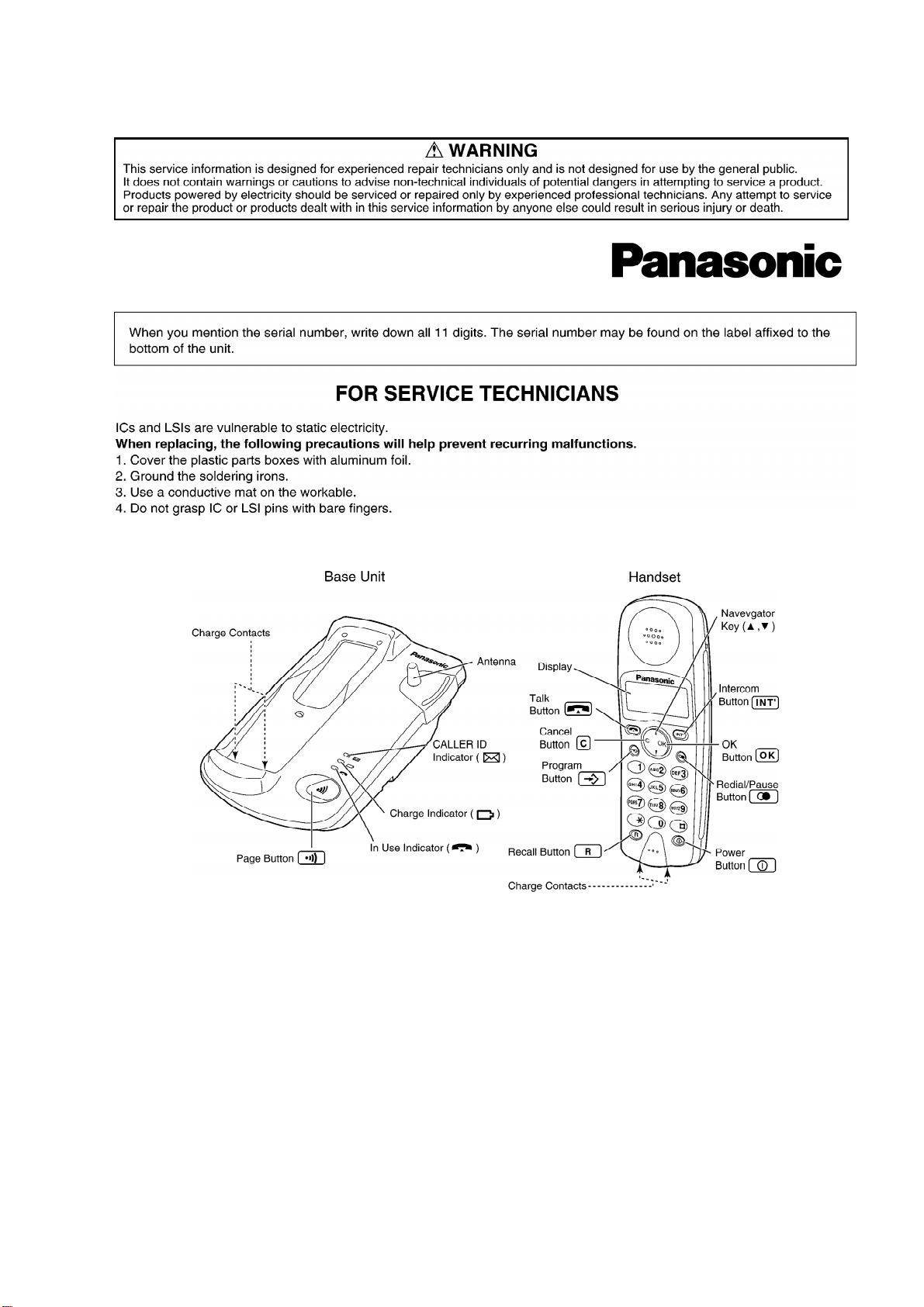
1. LOCATION OF CONTROLS
2

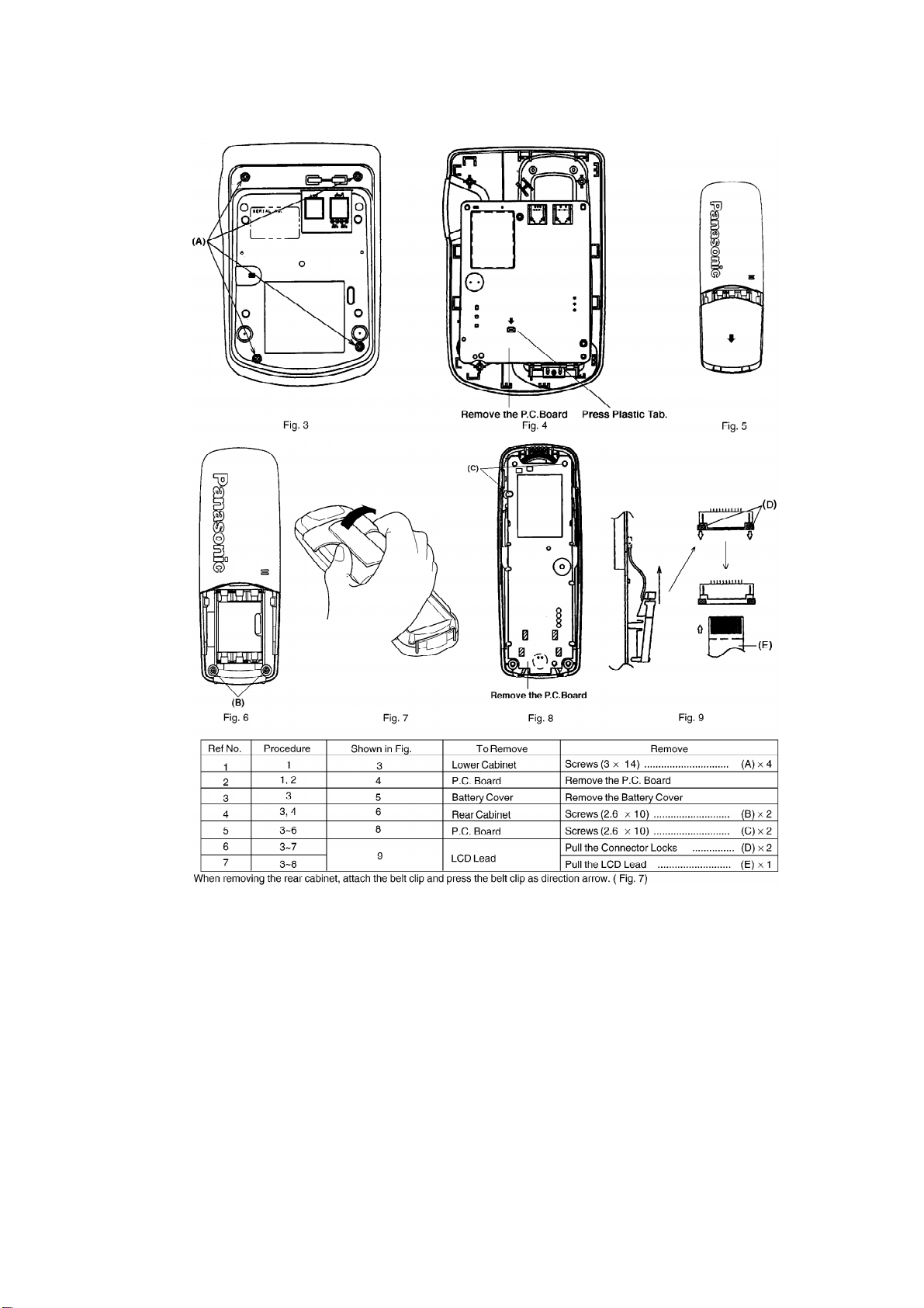
2. DISASSEMBLY INSTRUCUTIONS
3

3. SETTINGS
3.1. INSTALLING THEBATTERIES INTHEHANDSET
Install the batteries as shown. Theninstall the handset cover.
4

-Ifthe rechargeablebatteries are not inserted correctly, the handset
will not work.
3.2. CONNECTION
Plug inthe AC adaptorcordand the telephone line cordtothe bottomof the unit. Thenconnect
the cords as shown.
-USE ONLY WITHPanasonicAC ADAPTORKX-TCA11CE.
-Becareful not to confuse the telephone line jack with the AC
adaptor jack on the base unit. Ifconnected improperly, the base
5

unitwill not work and damage mayoccur.
-The AC adaptor must remainconnected at all times. (Itisnormal
for the adaptor to feel warm during use.)
-The unitwill not work during apower failure. We recommend you
connect astandard telephone on the same line for power
protection.
-Ifyour unitisconnected to aPBXwhich does not support Caller ID
services, you will not be ableto access those services.
3.3. BATTERYCHARGE
6

3.4. INSTALLING THEHANDSET CLIP
You canhang the handset on yourbelt orpocket using the belt clip.
7

4. OPERATIONS
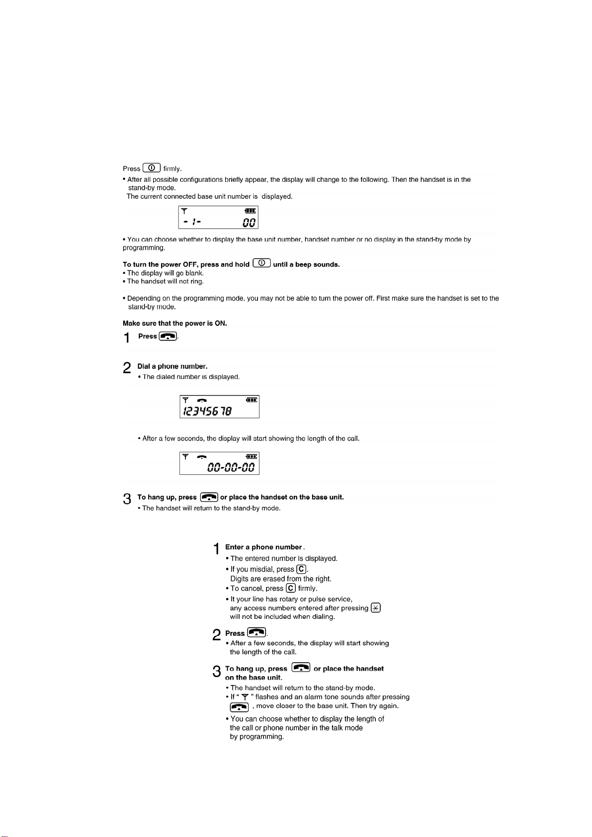
4.1. MAKING CALLS
4.1.1. TURNING THE POWER ON
4.1.2. TO DIALAFTER CONFIRMING THE ENTERED NUMBER
8

4.1.3. TO REDIALTHE LASTNUMBER DIALLED
4.1.4. TO REDIALAFTER CONFIRMING THE NUMBERS IN REDIALMEMORY
4.2. ANSWERING CALLS
4.3. SETTING THERECEIVERVOLUME
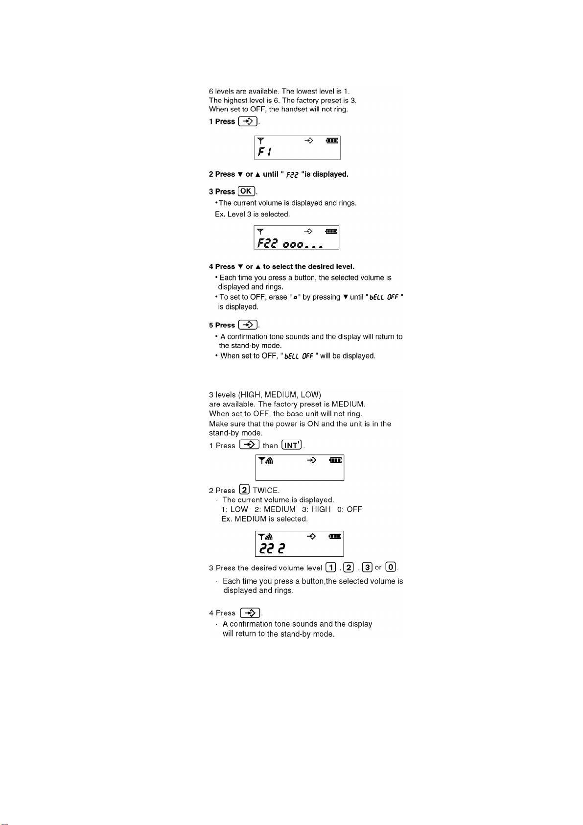
4.4. SELECTING THEHANDSET RINGERVOLUME
9

4.5. SELECTING THEBASE UNITRINGERVOLUME
5. HOW TO REPLACE THE RF UNIT OF HANDSET
Whenreplacing the P.C. BoardNo. PQUP10927ZB and PQUP10927YA, the hotmelt removing
and putting operation is required.
1. Cool the P.C. Board inthe freezer for 10 minutes, then remove the
hotmeltof the hatched parts inFig. 16 with the tipof minus
10

screwdriver.
2. Remove the solder of each pinon RFunit, then remove the RF
unitfrom the P.C. Board.
3. After soldering the new RFuniton the P.C. Board surely, put the
hotmelton the hatched part inthe Fig. 16.
4. Note: / Above-mentioned hotmeltremoving and putting operation
isonlyfor the P.C. Board No. PQUP10927ZBand PQUP10927YA.
5. There isno need of the hotmeltremoving and putting operation
for the PCBoard No. PQUP10927ZC.
6. BLOCK DIAGRAM RF UNIT (BASE UNIT)
11

7. BLOCK DIAGRAM BASEBAND SECTION AND
LINE INTERFACE (BASE UNIT)
12

8. CIRCUIT OPERATION (BASE UNIT)
8.1. R.F. SECTION(SEE BLOCK DIAGRAMFig. 17)
8.2. THEBASE-BAND SECTION(SEE BLOCK DIAGRAMFig. 18)
8.2.1. INTRODUCTION
13

The base-band section consists of a base-band integratedcircuit (BBIC), a FlashPROM, an
EEPROM, and anAND Gate.
8.2.2. THE BASE-BAND INTEGRATED CIRCUIT(BBIC)
The PQVINSC14424 (IC101) is a CMOS device designedtohandle all the audio, signal and data
processing neededina DECTbase unit. It contains a "burst mode controller” microprocessor
whichtakes care of DECTspecific physical layerand radiosection control. It alsocontains two
ADPCM transcoders, a lowpower14 bit codec (ADC/DAC), various otherADC´s, DAC´s and
timers, a gaussianfilterforthe DECTGFSK modulation method, clock and data recovery
circuits, a clock oscillatorcircuit, a DTMFgenerator(DSP), anecho suppression circuit (DSP),
and a pairof gaincontrollable audioamplifiers forline input and line output and a general
purpose microcontroller. / The IC101 interfaces toits external PROM (IC102) via a data/address/
control bus. It connects tothe EEPROM via a serial interface, and a second serial interface is
usedduring manufacture and service toconnect toanexternal computer.
8.2.3. FLASH PROM (SEE Fig. 19)
The 1 Mbit (IC102) FlashPROM contains the operational firmware forthe microcontroller. It is
interfacedtothe data/address/control bus using address lines A0 toA16, data lines D0 toD7,
and chipselect (pin30), output enable (pin32), and write (pin7).
8.2.4. EEPROM (SEE Fig. 19)
The electricallyerasable PROM PQVINM4C32L(IC103) is usedtostore all the temporary
operating parameters forthe base (see EEPROM LAYOUT). It uses a two-line serial data
interface withthe BBIC, withbi-directional data on pin5 (TP94), and clock on pin6 (TP93).
8.2.5. CLOCK GENERATION (SEE Fig. 19)
A single clock generatorinthe BBIC uses anexternal crystal X101 toderive all clock
frequencies usedinthe base. The crystal is tunedtothe exact frequencyof 10.368 MHz during
manufacture byfeeding a DC voltage froma DAC inthe microcontroller(frompin14 of IC101) to
the varicapdiode D104 (TP112). / The BBIC provide bufferedclock signals RFCLK (pin11,
TP139) at 10.368 MHZforthe FrequencySynthesizer, whichis onlyactive during the PLL lock
period. Otherclock is SCLK on pin1 (3.456MHz). The basic data rate forTRADATand RECDAT
is 1.152 Mbits/s, whichis 10.368 MHs dividedby9. The data rate forthe serial interface tothe
phase-lock-loop is also1.152 Mbits/s.
Circuit Diagram
14

8.2.6. LOCATOR KEY (SEE Fig. 19)
The keyboard“Locator(Page)” button is connectedtopin68 (TP154) of the IC101. When
pressedthe base transmits a message tothe handset, whichthenbeeps.
8.2.7. FACTORY SERIALPORT(SEE Fig. 19)
Inordertocommunicate withthe handset during manufacture and servicing (using a PC) a
serial data link has beenprovided. Serial data input/output is providedon J102 (TP151), and a
15

ground is providedon J103. The bi-directional serial data line is split intotwoat IC101 pin27
(input) and pin26 (output). Data rate is 9600 baud J103. D105provides ESD protection, and R117
and C146 provide RFde-coupling.
8.2.8. BUZZER CIRCUIT(SEE Fig. 19)
A square-wave signal fromIC101 pin41 (TP103) is usedtosound the buzzervia switching
transistorT101 (TP101). Various tones and cadences are useddependent on function. Buzzer
volume is variedbychanging the dutycycle of the drive waveform. D101 provides quenching of
back-emf generatedwhenT101 turns off.
8.2.9. OFF HOOK AND CALLER LED´S (SEE Fig. 19)
Whenthe Handset is in“Talk” mode, the Off-Hook LED D102 is switchedon bytransistorT102
(on), using a control line frompin28 of IC101 (TP106). “Onthe TCD952 the caller” LED is
switchedvia T103.
8.2.10. AUDIO PATH-RX AUDIO-LINE INPUT(SEE Fig. 20)
Audiofromthe Line Interface TXAF(TP123) enters the BBIC on pin58. R111 and C113 are to
balance the line input amplifier, intothe ADC part of the codec, where it is sampledand turned
intodigital data. The burst mode controllerthenprocesses this rawdata (calledthe B-field)
performing encryption and scrambling, adding the various otherfields that go togetherto
produce the GAP standardDECTframe, assigning toa time slot and channel etc. The data then
passes through the gaussianfiltertoemerge on pin22 as TRADAT, (TP132).
8.2.11. AUDIO PATH - TX AUDIO - LINE OUTPUT(SEE Fig. 20)
Audiofromthe receiverRECDATenters the BBIC on pin20 and passes through the clock
recoverycircuit. The burst mode controllerseparates out the B-fielddata, and performs de-
encryption and de-scrambling as required. It thengoes tothe DAC part of the codec where data
is turnedback intoanalogue audio. The audiosignal is amplifiedbythe gain-controlledline
output amplifier, and balancedaudiois output on pin63, and fedas RXAF(TP120) tothe Line
Interface.
Circuit Diagram
16

8.3. THELINEINTERFACESECTION(SEE BLOCK DIAGRAMFig. 19)
8.3.1. INTRODUCTION
This section consists of the telephone line interface, bell detector, hookswitch, pulse dialing
circuits, audiocircuits, DC mask & line impedance circuits, powersupplies, and batterycharger
circuits.
8.3.2. TELEPHONE LINE INTERFACE (SEE Fig. 21)
The telephone line is connected(via 2 or3 jumpers selectedforcountryof destination) toa
bridge rectifierD8. Surge suppressorSA3 protects against excessive line voltages. Test points
are TP14 (A), TP13 (B), TP21 (S) and TP15 (E). Bridge rectifierD8 provides forlines of either
polarity. The output of D8 is “Line +” (TP50) and “Line -” whichis ground.
8.3.3. EARTH RECALL (SEE Fig. 21)
Forcountries that require EarthRecall facilities, relayRLY1 is providedtoshort the E line tothe
17

A orB lines. The relayis energisedwhentransistorT2 is switchedon bya high level on the
EARTH control line (TP77) fromthe BB-IC IC101. D1 will quenchthe large back-emf voltage that
wouldotherwise occuracross the relaycoil whenT2 turns off.
8.3.4. BELL DETECTOR (SEE Fig. 21)
The AC ringing signal is detectedbyoptocouplerIC2, using its internal diode inconjunction
withD4. DC fromthe line is blockedbythe wall plug inside. The othercomponents D2, D3, and
R3 reduce current and increase the circuit impedance inline withnational requirements. When
ringing is detectedIC2 will turnon, and the RING line (TP76) will be draggedtoa lowvoltage.
Circuit Diagram
8.3.5. CLIP CIRCUITS (SEE Fig. 21)
The callerID signal is detectedbyIC4.
8.3.6. HOOKSWITCH (AND PULSE DIALING) (SEE Fig. 22)
T8 is the hookswitch, drivenbyT9. Whenthe phone is “off-hook”, the HOOK control signal from
the BBIC will be a high logic level (+3V), and all bothtransistors will be on, thus T8 will “loop”
the line. The zennerdiode D10 protects transistors T11 toT13 against transient line voltages.
8.3.7. PULSE DIALING (SEE Fig. 22)
During pulse dialing the hookswitch(T8, T9) is usedtogenerate the pulses using the HOOK
control signal, whichis set high during pulses. To force the line impedance lowduring the
“pause” intervals betweendial pulses, the PAUSE-DIALsignal turns on T11, whichturns on T12
harder(increases current), thus reducing line impedance (see 8.3.10. BATTERY CHARGER)
8.3.8. AUDIO CIRCUITS (SEE Fig. 22)
The line output signal fromthe BBIC RXAF(TP120) is amplifiedbyT13. The RXAFline is DC
coupledtoT13 thus making it work as a current limiter(typically< 8mA). The emitterloadof T13
18

is complex toachievedthe correct frequencyresponse, since the line load(forUK) is also
complex. The line input signal TXAF(TP123) is takenfromthe junction of R41 and R70. Phase
cancellation of the line output audiooccurs at this point, sothat onlyincoming line audio
shouldbe passedtothe BBIC on TXAF.
Circuit Diagram
8.3.9. POWER SUPPLIES (SEE Fig. 23)
The AC Adaptorforthe KX-TCD952GB consists of twoseparate isolatedDC supplies providing
a +8 V supplyforthe base circuitry, and a 9 V supplyonlyforthe chargercircuit. The isolation is
because the mainbase circuitryis connectedtothe telephone line, sopotentiallyhazardous
voltages maybe present, while the chargercircuitryhas charge contacts that couldbe touched
bythe operator, sothe twosupplies must be kept separate. The 8 V supplyfromthe AC Adaptor
is connectedvia J2 pin1 (TP90) +8 V, and J2 pin2 (TP89) ground. The unregulated+8 V supply
is fedtothe first regulator.This regulatorIC7 provides a regulatedoutput pin2 (TP91) of +4.0 V
(called+4V). The second regulatorIC6 is fedwith+4V and provides the stable +3.0V supply
(TP95). During power-up this regulatorgenerates a RESETsignal (TP94) whichis usedtoreset
the microcontrollerand BBIC.
8.3.10. BATTERY CHARGER (SEE Fig. 23)
The 9 V supplyfromthe AC Adaptoris connectedvia J2 pin6 (TP82) positive, and J2 pin5
(TP78) negative. Theconstant current batterychargercircuit is made up of T14 and T15 (series
pass transistor) and associatedcomponents. Charging detectorcircuit T16 switches on whena
charging current flows through R64 and D11, and turns on the “Charging” LED D12. The charge
contacts are J3 (TP89) positive and J4 (TP88) negative.Charge current flows invia J4, through
T15, R63, AC Adaptor9 V supply, R64, D11, and out via J3.
Circuit Diagram
19

9. BLOCK DIAGRAM RF UNIT (HANDSET)
20
Table of contents