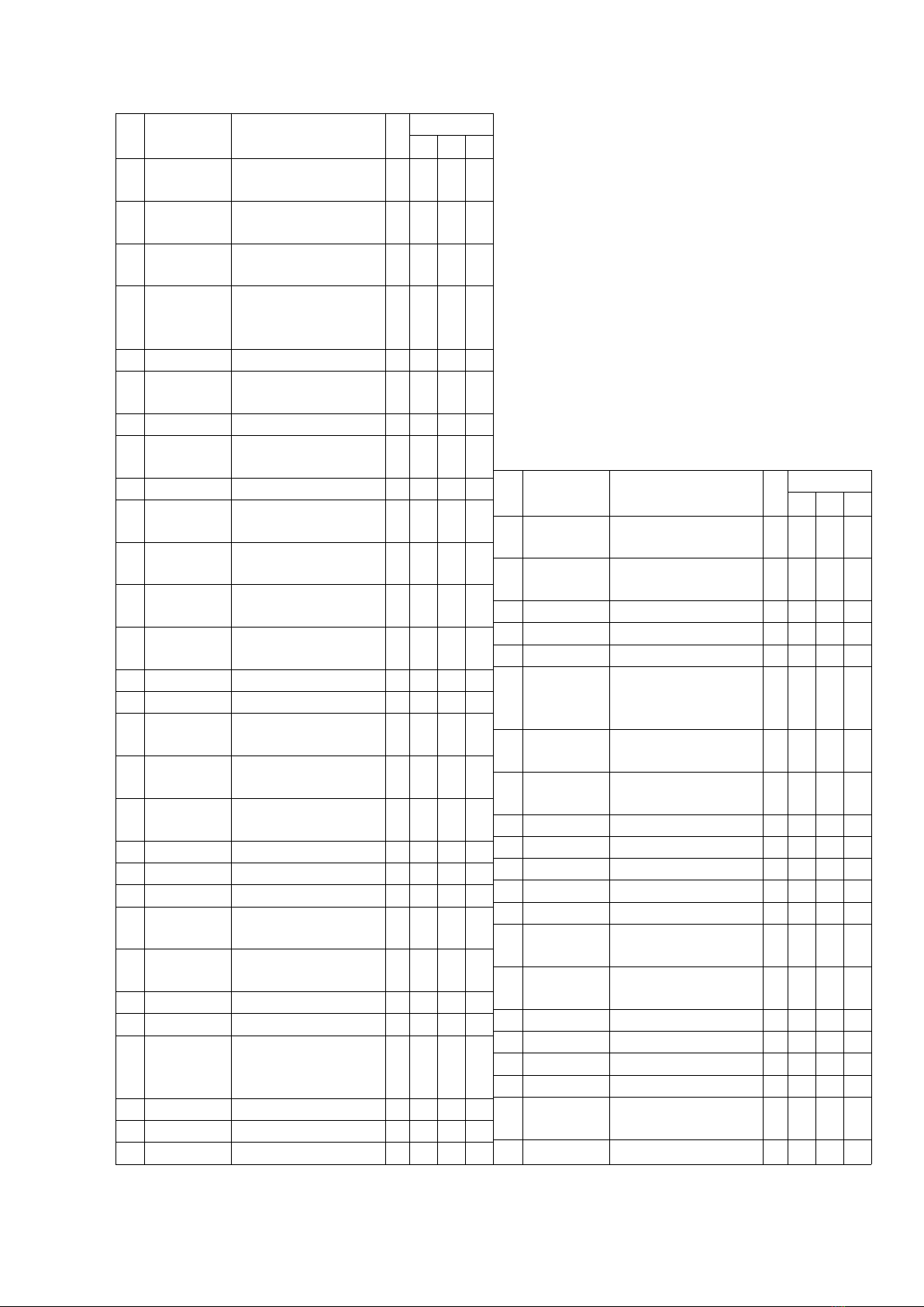
Matsushita Electric CQ-C8403W User manual

ORDER NO. ACED051233C3
AUTOMOTIVE AFTERMARKET
CQ-C8403W
WMA MP3 CD Player/Receiver
SPECIFICATIONS
Specifications*
General
Power Supply DC 12V (11V - 16V),
Test Voltage 14.4V
Negative Ground
Tone Controls (Bass/
Treble)
Bass: ±12dB at 60Hz / Treble: ±
12dB at 16kHz
Equalizer Center Frequency 60, 160, 400, 1k, 3k, 6k, 16k (Hz)
Variable Range of Equalizer -12dB to 12dB (2dB step)
Current Consumption Less than 2.2A / (CD mode; 0.5W × 4
-speaker)
Maximum Power Output 50W × 4(at 1kHz)
Speaker Impedance 4 - 8
Pre-amp Output Voltage 5V (CD mode; 1kHz, 0dB)
Subwoofer Output Voltage 5V (CD mode; 1kHz, 0dB)
Pre-amp Output Impedance 60
Subwoofer Output
Impedance
60
FM Stereo Radio
Frequency Range 87.50MHz - 108.00MHz
Usable Sensitivity 6dB/ V (S/N 30dB)
Stereo Separation 35dB (at 1kHz)
AM Radio
Frequency Range 531kHz - 1,602kHz
Usable Sensitivity 28dB/ V (S/N 20dB)
CD Player
Sampling Frequency 8 Times Oversampling
1

DA Converter 4 DAC System
Pick-up Type Astigma 3-Beam
Light Source Semiconductor Laser
Wave Length 790 nm
Frequency Response 20Hz-20kHz (±1dB)
Signal to Noise Ratio 96dB
Total Harmonic Distortion 0.01% (1kHz)
Wow and Flutter Below Measurable Limits
Channel Separation 75dB
Dimensions (W×H×D)** 178×50×155mm
Weight** 1.6 kg
* Specifications and the design are subject to possible
modification without notice due to improvements.
** Dimensions and Weight shown are approximate.
** Above specifications comply with EIA standards.
2005 Matsushita Electric Industrial Co., Ltd. All rights reserved.
Unauthorized copying and distribution is a violation of law.
1. ABOUT LEAD FREE SOLDER (PbF)
Distinction of PbF PCB:
PCBs (manufactured) using lead free solder will have a PbF stamp on the PCB.
Caution :
- Pb free solder has a higher melting point than standard solder; Typically
the melting point is 50 - 70°F (30 - 40°C) higher. Please use a soldering
2

iron with temperature control and adjust it to 700 ± 20°F (370 ± 10°C). In
case of using high temperature soldering iron, please be careful not to
heat too long.
- Pb free solder will tend to splash when heated too high (about 1100°F/
600°C)
- This lead free solder will be used for the products after serial No.
1,000,001.
2. FEATUERS
- Hands-Free Phone System (The optional Bluetooth hands-free kit: CY-
BT100N).
- Expansion Module (The optional Hub unit: CY-EM100N).
- The optional adapter allows you to connect the optional Panasonic DVD
changer unit (CX-DH801N).
- The optional adapter allows you to connect the optional Panasonic CD
changer unit (CX-DP880).
- The optional adapter allows you to connect the optional iPod series.
- SQ (Sound Quality).
- SQ7 (7-Band Sound Quality) .
- D.M(Direct Memory).
- Customize the Display (Customize Function).
- MP3/WMA Playback from CD-R/RW.
3. REPLACEING THE FUSE
Use fuses of the same specified rating 15 amps. Using different substitutes or fuses with higher ratings,
or connecting the unit directly without a fuse, could cause fire or damage to the stereo unit.
4. MAINTENANCE
Your products is designed and manufactured to ensure a minimum of maintenance. Use a soft cloth for
routine exterior cleaning. Never use benzine, thinner or other solvent.
5. NOTES
[RADIO BLOCK]
Do not align the AM/FM package block. When the package block is necessary, it will be supplied already
aligned at the factory.
[CD DECK BLOCK]
This model has no servo alignment points because microcomputer controls the servo circuit
6. DIMENSIONS
3

7. LASER PRODUCTS
8. WIRING CONNECTION
4

9. DISASSEMBLY INSTRUCTIONS
9.1. How to Remove the Flexible PCB(AP2)
5

9.2. How to Install the Main P.C.B. of the Electric Display
10. TERMINALS DESCRIPTION
10.1. Main Block
IC601 : C2CBKG000034
6

Pin
No.
Port Description (I/
O)
(V)
FM AM CD
1 PANEL
OPEN
Panel open
detection
I 0 5.2 5.2
2 PANEL
CLOSE
Panel close
detection
I 0 0 5.2
3 SUBM CNT 3.3V power control
for Display
O 5.0 - -
4 BATT Battery power
check
I 4.8 5.0 5.0
5 ACC Acc. power check I 4.8 5.0 5.0
6 SDA Serial data for
electronic volume
I/O 4.9 4.9 4.9
7 SCLK Serial clock for
electronic volume
O 4.9 4.9 4.9
8 CD MUTE Signal mute from
CD deck
I 5.0 5.0 5.0
9 Vss GND - 0 0 0
10 ST FM stereo detection I 5.1 5.2 5.2
11 PLL DI
(MO)
Serial data to PLL O 0.6 0 0
12 PLL DO
(MI)
Serial data from PLL I 5.2 5.2 5.2
13 PLL CLK Serial clock for PLL O 4.9 4.9 4.9
14 PLL CE Chip enable for PLL O 0 0 0
15 CD RESET Reset for CD deck O 4.9 4.9 4.9
16 SUB SI Serial data to
Display CPU
O 0.6 0.6 0.8
17 CD IN Disc-in detection I 5.0 5.0 5.0
18 SUB SO Serial data from
Display CPU
I 4.4 4.4 4.4
19 CH DATA/
UP SO
XM SO/UP SO Serial
data from Changer
I 1.6 1.6 1.6
20 CH CLK/
UP CLK
Serial clock for
Changer or Flash
writer
I 4.9 4.9 4.9
21 Vdd +5V power supply - 4.9 4.9 4.9
22 XM SI (MO)
/ UP SI
Serial data to
Satellite or Flash
writer
O 0 0 0
23 CD SI (MO) Serial data to CD
deck
O 0 0 0
24 CD SCLK Serial clock for CD
deck
I/O 0 0.4 0
25 CONDENSOR
Capacitor
connection for
power
- 3.3 3.3 3.3
26 CD SO (MI) Serial data from CD
deck
I 0 0 0
Pin
No.
Port Description (I/
O)
(V)
FM AM CD
27 CH STB Strobe from
Changer
I 0 0 0
28 CH REM
OUT
Remote control
codes to Changer
O 4.9 4.9 0.4
29 DECK V
CONT
Power control for
CD deck
O 4.9 4.9 4.9
30 REMO INT Interrupt for remote
control
I 3.7 3.7 3.7
31 CD FS Frame sync. for CD
deck
O - - -
32 Avdd +5V power supply - 5.1 5.1 5.1
33 AVREF +5V power supply - 5.1 5.1 5.1
34 AVGND GND - 0 0 0
35 AVSS GND - 0 0 0
36 SD FM/AM signal level
meter
I 0.2 0 0.3
37 INIT A Model setting A by
voltage level
I 0 0 0
38 INIT B Model setting B by
voltage level
I 0 0 0
39 A IN Spectrum analyzer
data
I 0 0 0
40 Vss GND - 0 0 0
41 SYS ID1 Hub connection
device detection ID
1
I 0 0 0
42 SYS ID2 Hub connection
device detection ID
2
I 5.2 5.2 5.2
43 HUB
EVENT
Bluetooth incoming
detection
I 5.2 5.2 5.2
44 HUB CNT Request of hub
connection check
O 0 0 0
45 CD SW1 Disc detection
switch 1
I 0 0 0
46 CD SW2 Disc detection
switch 2
I 0 0 0
47 MOD0 Operating mode
control 0 from
Flash writer
I 5.1 5.1 5.1
48 MOD1 Operating mode
control 1: pulled up
to H
- 5.1 5.1 5.1
49 MOD2 Operating mode
control 2 from
Flash writer
I 0 0 0
50 H
STANDBY
Standby control
from external
I 5.0 5.0 5.0
7

Pin
No.
Port Description (I/
O)
(V)
FM AM CD
51 DCDC
CONT
Not connected - - - -
52 FP
MOTOR1
Open/Close of
Front panel 1
O 4.9 5.0 4.9
53 FP
MOTOR2
Open/Close of
Front panel 2
O 4.9 5.0 4.9
54 V CONT1 Reference voltage
control for motor
driver
O 0 0 5.0
55 REMO 1 Remote control data I 5.0 5.0 5.0
56 SA CLK Spectrum analyzer
clock
O 5.0 5.0 4.9
57 EXT MUTE Pulled up to H I 5.3 5.2 5.2
58 AMP CONT Power control for
external Amplifier
O 4.9 5.0 4.9
59 BZ OUT Buzzer signal O 0 0 0
60 OEL
VCONT
Power control for
OEL
O 0 0 0
61 WOW
MODE1
SRS WOW mode 1
(C8403U only)
O 0 0 0
62 WOW
MODE2
SRS WOW mode 2
(C8403U only)
O 0 0 0
63 WOW
MODE3
SRS WOW mode 3
(C8403U only)
O 0 0 0
64 DIM1 Not connected - - - -
65 DIM2 Not connected - - - -
66 MAIN CNT2 Power control for
Hub
O 5.0 5.0 5.0
67 SRC KEY SOURCE key
detection
I 5.0 4.9 5.0
68 PANEL IN Panel attachment
detection
I - - -
69 NC Not connected - - - -
70 NC Not connected - - - -
71 NC Not connected - - - -
72 MAIN
CONT
Main power control O 4.9 4.9 4.9
73 INV CONT Dimmer power
control
O 5.0 5.0 5.0
74 AF MUTE Audio mute O 5.0 5.0 5.0
75 RESET Reset I 5.0 5.0 5.0
76 FOCUS
ELV
Focus elevation for
SRS WOW (C8403U
only)
O - - -
77 X1A Oscillator clock O 2.1 2.1 2.1
78 X0A Oscillator clock I 1.6 1.6 1.6
79 Vss GND - 0 0 0
Pin
No.
Port Description (I/
O)
(V)
FM AM CD
80 X1 Crystal oscillator
clock
I 2.0 2.0 2.0
81 X2 Crystal oscillator
clock
O 2.5 2.5 2.5
82 Vdd +5V power supply - 5.0 5.0 5.0
83 P00 Pulled down to L - 0 0 0
84 P01 Pulled up to H - 5.1 5.0 5.1
85 OFFSET
DET
Audio clipping level
detection from
Power amp.
I 0 0 0
86 STBY Standby for Power
amp.
O 5.0 5.0 5.0
87 MUTE Mute for Power
amp.
O 0 0 0
88 ILL SENS Pulled up to H - 5.0 5.0 5.0
89 NC Not connected - - - -
90 EP DO(MI)
91 NC Not connected - - - -
92 NC Not connected - - - -
93 SUB
RESET
Reset for display
CPU
O 4.9 5.0 4.9
94 DISPM
CONT
5V power control
for Display
O 0 0 0
95 NC Not connected - - - -
96 NC Not connected - - - -
97 NC Not connected - - - -
98 S LED Security LED drive O 0 0 5.0
99 ANT CONT Power control for
antenna motor
O 5.2 5.2 5.2
100 NC Not connected - - - -
8

10.2. Display Block
IC901 : C2CBKJ000195
Pin
No.
Port Part Name &
Description
I/O (V)
1 NC Not connected - -
2 DCLK SLV4 Slave D-CLK4 (Clock
for image data)
I 1.5
3 UART SS4 GND - 0
4 UART SS3 GND - 0
5 D DIS Disable for Anode
drive (Disable for
image signal)
O 0
6 PADJ IO2 Anode output pulse
width adjusting data 2
(Image data)
O 3.8
7 DCLK SLV3 Slave D-CLK 3 (Clock
for image data)
I 1.5
8 NC Not connected - -
9 NC Not connected - -
10 NC Not connected - -
11 KS1 Key scan 1 O 0
12 KS2 Key scan 2 O 0
13 KS3 Key scan 3 O 0
14 NC Not connected - -
15 BUS BYTE GND - 0
16 CNVSS CPU rewrite mode/
Single CPU mode
selection for Flash
writer
I 0
17 IADJ Anode output current
adjusting data
(Luminance control)
O 0
18 I CLK Clock for anode
output current
adjusting data
O 0
19 RESET Reset from main CPU I 4.4
20 X1 Ceramic oscillator
clock (8MHz)
O 2.5
21 GND GND - 0
22 X0 Ceramic oscillator
clock (8MHz)
I 2.2
23 VCC5.0V Power supply - 4.6
24 NMI Pulled up to H - 4.6
25 Y SYNC Cathode scan data
and Cathode latch
control (Vertical sync.)
O 0
26 NC Not connected - -
27 NC Not connected - -
9

Pin
No.
Port Part Name &
Description
I/O (V)
28 X SYNC Clock for Cathode
scan; or Latch strobe
for Anode output
pulse width adjusting
data and Anode
output current
adjusting data
O 0
29 A CLK TA Anode output pulse
width adjusting clock
O 2.7
30 NC Not connected - -
31 NC Not connected - -
32 S DIS Disable for Cathode
drive
O 2.4
33 NC Not connected - -
34 NC Not connected - -
35 NC Not connected - -
36 NC Not connected - -
37 NC Not connected - -
38 PADJ IO1/
TXD
Anode output pulse
width adjusting data 0
(Image data); or Serial
data for Flash writer
O 1.2
39 VCC5.0V Power supply - 3.3
40 RXD Serial data from Flash
writer
I 1.3
41 GND GND - 0
42 DCLK MST/
SCLK
Master D-CLK (Clock
for image data);or
Serial clock from
Flash writer
O/I 3.3
43 BUSY Busy for Flash writer O 1.5
44 OEL OE OEL output enable O 0
45 PADJ IO0 Anode output pulse
width adjusting data 0
(Image data)
O 1.8
46 DCLK SLV0 Slave D-CLK 0 (Clock
for image data)
I 2.7
47 UART SS0 GND - 0
48 NC Not connected - -
49 FLASH CE Chip enable for Flash
memory
O 1.7
50 NC Not connected - -
51 NC Not connected - -
52 RY/BY Pulled up to H - 3.6
53 NC Not connected - -
54 EPM Program mode enable
for Flash writer
I 2.3
55 NC Not connected - -
10

Pin
No.
Port Part Name &
Description
I/O (V)
56 NC Not connected - -
57 GND GND - 0
58 NC Not connected - -
59 VCC3.3V Power supply - 3.6
60 NC Not connected - -
61 NC Not connected - -
62 NC Not connected - -
63 FLASH OE Output enable for
Flash memory
O 3.6
64 NC Not connected - -
65 FLASH WE Write enable for Flash
memory
O 3.6
66 NC Not connected - -
67 NC Not connected - -
68 NC Not connected - -
69 NC Not connected - -
70 FLASH A22 A22 in Address bus O 0
71 FLASH A21 A21 in Address bus O 3.6
72 FLASH A20 A20 in Address bus O 3.6
73 FLASH A19 A19 in Address bus O 0
74 VCC3.3V Power supply - 3.6
75 FLASH A18 A18 in Address bus O 3.6
76 GND GND - 0
77 FLASH A17 A17 in Address bus O 0
78 FLASH A16 A16 in Address bus O 2.5
79 FLASH A15 A15 in Address bus O 0
80 FLASH A14 A14 in Address bus O 0
81 FLASH A13 A13 in Address bus O 2.5
82 FLASH A12 A12 in Address bus O 2.5
83 FLASH A11 A11 in Address bus O 0
84 FLASH A10 A10 in Address bus O 0
85 FLASH A9 A9 in Address bus O 0
86 FLASH WP Write protect/
Accelaration from
Flash memory
O 0
87 NC Not connected - -
88 NC Not connected - -
89 NC Not connected - -
90 NC Not connected - -
91 VDD 3.3V Power supply - 3.4
92 FLASH A8 A8 in Address bus O 0
93 GND GND - 0
94 FLASH A7 A7 in Address bus O 0
95 FLASH A6 A6 in Address bus O 0
96 FLASH A5 A5 in Address bus O 0.6
97 FLASH A4 A4 in Address bus O 3.0
98 FLASH A3 A3 in Address bus O 1.8
11

Pin
No.
Port Part Name &
Description
I/O (V)
99 FLASH A2 A2 in Address bus O 1.8
100 FLASH A1 A1 in Address bus O 1.8
101 FLASH A0 Not connected - -
102 FLASH D15 DQ15 in Data bus I/O 3.1
103 FLASH D14 DQ14 in Data bus I/O 0.6
104 FLASH D13 DQ13 in Data bus I/O 0.4
105 FLASH D12 DQ12 in Data bus I/O 0.4
106 FLASH D11 DQ11 in Data bus I/O 0.4
107 FLASH D10 DQ10 in Data bus I/O 0.4
108 FLASH D9 DQ9 in Data bus I/O 0.7
109 FLASH D8 DQ8 in Data bus I/O 1.6
110 FLASH D7 DQ7 in Data bus I/O 1.7
111 FLASH D6 DQ6 in Data bus I/O 1.6
112 FLASH D5 DQ5 in Data bus I/O 1.6
113 FLASH D4 DQ4 in Data bus I/O 1.6
114 FLASH
RESET
Reset for Flash
memory
O 3.4
115 NC Not connected - -
116 NC Not connected - -
117 NC Not connected - -
118 NC Not connected - -
119 FLASH D3 DQ3 in Data bus I/O 0
120 FLASH D2 DQ2 in Data bus I/O 1.8
121 FLASH D1 DQ1 in Data bus I/O 2.3
122 FLASH D0 DQ0 in Data bus I/O 2.2
123 NC Not connected - -
124 NC Not connected - -
125 SUB SI Serial data from main
CPU
I 0
126 SUB SO Serial data to main
CPU
O 0.8
127 ROTARY 1 Volume-up detection
from Rotary encoder
I 1.8
128 ROTARY 2 Volume-down
detection from Rotary
encoder
I 4.5
129 A CLK SCLK Anode output pulse
width adjusting clock
I 2.6
130 GND GND - 0
131 A CLK Anode output pulse
width adjusting clock
O 0.7
132 VCC5.0V Power supply - 4.5
133 KEY RET4 Key return 4 I 0
134 KEY RET3 Key return 3 I 0
135 KEY RET2 Key return 2 I 0
136 KEY RET1 Key return 1 I 0
137 OEL RESET Reset for OEL O 4.5
12

Pin
No.
Port Part Name &
Description
I/O (V)
138 NC Not connected - -
139 NC Not connected - -
140 AD AVSS GND - 0
141 TH DETECT Thermal detection I 1.7
142 AD VREF +5V Power supply - 4.5
143 AD AVCC +5V Power supply - 4.5
144 PADJ IO3 Anode output pulse
width adjusting data 3
(Image data)
O 1.2
10.3. CD Servo Block
IC101 : YESAM337
Pin
No.
Port Descriptions I/O (V)
1 AVSS GND - 0
2 LD-MT Loading Motor drive IC
control 1
O 3.2
3 CNT Loading Motor drive IC
control 2
O 3.2
4 - - - -
5 LD-EJ Loading Motor drive IC
control (Eject)
O 0
6 AMUTE Mute signal output O 0
7 - - - -
8 SBSY DSP IC SBSY O 0
9 - - - -
10 - - - -
11 TXD0 Serial data output O 0
12 RXD0 Serial data input I 0
13 CLK0 Clock input I 2.9
14 - - - -
15 - - - -
16 - - - -
17 AMD - - 3.2
18 DVCC Power supply (3.3V) - 3.2
19 X2 Crystal oscillator - 1.3
20 DVSS GND - 0
21 X1 Crystal oscillator - 1.3
22 AMI - - 3.2
23 RESET Reset I 3
24 - - - -
25 - - - -
26 NMI - - 3.2
27 - - - -
28 STBY DSP IC STBY O 0
29 RST DSP IC RST O 3.2
13

Pin
No.
Port Descriptions I/O (V)
30 CCE DSP IC CCE O 2.6
31 BUCK DSP IC CK O 2.8
32 BUS3 DSP IC BUS3 O 2.8
33 BUS2 DSP IC BUS2 O 2.8
34 BUS1 DSP IC BUS1 O 2.8
35 BUS0 DSP IC BUS0 O 2.9
36 RESET
SW
Mechanics deck REST
SW input
I 3.2
37 SW1 Mechanics deck SW1
input
I 0
38 SW2 Mechanics deck SW2
input
I 0
39 CONT
(P13)
DSP IC power control 1 O 3.2
40 - - - -
41 - - - -
42 - - - -
43 CONT
(P17)
DSP IC power control 2 O 3.2
44 PIO0 DSP IC PIO0 O 0
45 ZDET LOAD detect I 0
46-48 - - - -
49 FLASH CE - - 3.2
50-58 - - - -
59 CDFS Serial frame sink signal
input (CD ON)
I 2.3
60 P50/AN0 Reference voltage I 0.3
61 P51/AN0 Loading motor detect I 2.1
62 P52/AN2 - - 0
63 P53/AN3 - - 0
64 AVCC Power supply (3.3V) - 3.2
11. IC BLOCK DIAGRAM
11.1. Main Block
IC201 : C1BB00000796
14

IC231 : C0JBZS000003
15

IC670 : C0JBAZ000904
IC730 : C0DAEKG00002
IC701 : C0DAZHF00004
16

IC755 : C0DBZGD00040
IC760 : C0GBG0000032
IC770 : C0DBAHG00020
17

11.2. CD Servo Block
IC401,403 : YESAM341
IC402 : YESAM342
12. REPLACEMENT PARTS LIST
Notes :
1. Be sure to make your orders of replacement parts according to this list.
2. Important safety notice: Components, identified by mark have
special characteristics important for safety. When replacing any of
these components, use only manufacturer's specified parts.
3. Location keys in the remarks column indicates the general location of
the parts shown in the exploded drawing, as in a road map.
4. The marking (RTL) indicates that Retention Time is limited for this item.
18

After the discontinuation of assembly in production, the item will
continue to be available for a specific period of time. The retention
period of availability is dependent on the type of assembly, and in
accordance with the laws governing part and product retention. After
the end of this period, the assembly will no longer be available.
- Order intake period is basically six months after the first shipment.
5. “T” marks in remarks colum are indicated supply parts of PTW.
Ref. No. Part No. Part Name & Description Remarks
[E3108] Main/Sub Block
IC's AND TRANSISTORs
IC201 C1BB00000796 IC T
IC221 C1BB00001131 IC T
IC231 C0JBZS000003 IC T
IC251 C0ABBA000221 IC T
IC252 C0ABCA000121 IC T
IC271 C1ZAZ0001450 IC T
IC401 C1BB00001045 IC T
IC601 C2CBKG000034 IC T
IC650 C0JBAA000372 IC T
IC670 C0JBAZ000904 IC T
IC701 C0DAZHF00004 IC T
IC702 C0EBZ0000035 IC T
IC730 C0DAEKG00002 IC T
IC752 C0CBCBG00012 IC T
IC755 C0DBZGD00040 IC T
IC760 C0GBG0000032 IC T
IC770 C0DBAHG00020 IC T
IC790 C0CBCYG00004 IC T
PA51 C5BA00000123 Electronic Tuner T
Q55 B1GDGFEH0001 Transistor T
Q56 B1AAEC000002 Transistor T
Q220 B1GBCFNN0004 Transistor T
Q235 B1GBHBEA0004 Transistor T
Q241 B1GBHBEA0004 Transistor T
Q251 B1GBHBEA0004 Transistor T
Q252 B1GBHBEA0004 Transistor T
Q320 B1GBCFNN0004 Transistor T
Q335 B1GBHBEA0004 Transistor T
Q341 B1GBHBEA0004 Transistor T
Q351 B1GBHBEA0004 Transistor T
Q352 B1GBHBEA0004 Transistor T
Q353 B1GBHBEA0004 Transistor T
Q354 B1GDCFJJ0002 Transistor T
Q371 B1GBCFNN0004 Transistor T
Q372 B1GBCFJN0004 Transistor T
Q376 B1GBCFNN0004 Transistor T
Q411 B1CBGF000005 Transistor T
Q630 B1GBCFNN0004 Transistor T
Q633 B1GDCFJJ0002 Transistor T
Q650 B1GBCFJN0004 Transistor T
Q651 B1GBCFJN0004 Transistor T
19

Ref. No. Part No. Part Name & Description Remarks
Q652 B1GBCFJN0004 Transistor T
Q680 B1GDGFEH0001 Transistor T
Q681 B1GDCFJJ0002 Transistor T
Q701 B1BACF000026 Transistor T
Q760 B1GBCFNN0004 Transistor T
Q771 B1ABCF000187 Transistor T
Q791 B1GBNCEJ0003 Transistor T
Q793 B1GBCFJN0004 Transistor T
DIODEs
D201 B0JCME000012 Diode T
D202 B0JCME000012 Diode T
D203 B0JCME000012 Diode T
D204 B0JCME000012 Diode T
D251 B0JCMC000004 Diode T
D301 B0JCME000012 Diode T
D302 B0JCME000012 Diode T
D303 B0JCME000012 Diode T
D304 B0JCME000012 Diode T
D601 B0JCMC000004 Diode T
D630 B3AAB0000143 Diode T
D631 YEADUDZS56BT Diode T
D632 MA3X152D0L Diode T
D635 YEADUDZS56BT Diode T
D636 YEADUDZS56BT Diode T
D637 YEADUDZS56BT Diode T
D638 YEADUDZS56BT Diode T
D639 YEADUDZS56BT Diode T
D670 B0JCMC000004 Diode T
D680 MA3X152A0L Diode T
D701 B0BA04700003 Diode T
D702 MA2Q73600L Diode T
D703 B0BC5R7A0062 Diode T
D704 B0JCMC000004 Diode T
D705 B0ECKP000002 Diode T
D706 B0ECKP000002 Diode T
D707 B0JCPE000004 Diode T
D708 MA2Q73600L Diode T
D710 B0JCMC000004 Diode T
D715 MA3X152A0L Diode T
D716 MA3X72100L Diode T
D751 B0ECKP000002 Diode T
D752 B0ECKP000002 Diode T
D760 B0BC5R000020 Diode T
D761 B0BC3R0A0058 Diode T
D770 B0JCMC000004 Diode T
D771 B0JCQD000002 Diode T
D772 B0BC013A0063 Diode T
CAPACITORs
C52 F1J1H470A025 Ceramic, 47PF 50WV T
C53 F1J1H103A513 Ceramic, 0.01 F 50WV T
C54 F2A1A221A449 Electrolytic, 220 F 10WV T
20
Table of contents