MediaQ MQ-1168 User manual

MQ-1168 Evaluation Board Users Guide MediaQ Incorporated
Board Revision 2
Revision A 4/18/02 Preliminary 1
MQ-1168 Evaluation Board Users Guide
Board Revision 2

MQ-1168 Evaluation Board Users Guide MediaQ Incorporated
Board Revision 2
Revision A 4/18/02 Preliminary 2
INTRODUCTION
This guide is intended to give a brief overview of the MQ-1168 and describe the features and workings of
the MQ-1168 / PCI Evaluation Board. This includes how to locate connectors, configure switches,
configure jumpers, and the initialization and configuration of this Evaluation board with the PC
motherboard with PCI interface as well as other platforms by using special adapters.
MQ-1168 OVERVIEW
The MQ-1168 is the second generation product in the MQ-11xx series from MediaQ. This device
provides rich video and audio functions in addition to high performance graphics and high speed
peripherals designed to give the user a complete multimedia experience. The MQ-1168 integrates a 64-bit
2D graphics engine, a flexible LCD display interface, dedicated Video Input port (VI), Secure Digital
interface (SD), Serial Peripheral Interface (SPI), AC-97/I2S audio and USB controllers (function and host)
on a single chip. The MQ-1168 has a 64-bit wide internal bus to 320KBs of embedded memory providing
scalable bandwidth of up to 384MB/sec for the frame, video, USB and audio buffers. The MQ-1168
directly supports connection to the Intel SA-1110 and PXA2x0, the Motorola Dragonball series, the NEC
VR-4100 family and the Hitachi SH-3/SH-4 CPUs as well as 32bit PCI.
PLATFORM DESCRIPTION
When installed into a PCI slot of a standard PC motherboard, the Evaluation Board can provide a
development and verification platform for hardware and software. Using an adapter card, specified at the
time of order placement, the Evaluation board can also be used in conjunction with other development
environments. Adapters are currently available for the Intel PXA2X0 Lubbock, SA-1110/1111
Assabet/Neponset, Palm Hurricane, Hitachi S1 (or equivalent) and NEC VR4121 Falcon development
platforms.

MQ-1168 Evaluation Board Users Guide MediaQ Incorporated
Board Revision 2
Revision A 4/18/02 Preliminary 3
EVALUATION BOARD LAYOUT
The location of the connectors, jumpers and other notable features are shown on the layout diagram
below. These are described in the tables on the following pages.
USB
Device
USB
Host
MQ-
1168
U1 J2
U28
SD/MMC
Generic CPU Connector
Audio Expansion
V
I
P
C
o
n
n
S-Video
RCA
Bt835
Video Decoder
Generic FP
Generic FP Large Formfactor
Audio
In
Audio
Out
I2S
CODEC
AC97
CODEC
Video Clock &
Sync Option
Area
Main
Audio
CODEC
Selection
Area
J1 JS1 J7
J3
J5
J2
JP1
JP4
JP3
JP7
JP5
JP6
JP2 J10
J8
D2
U3
CN1
CN2
CN3 J9
U27
U29
CN5
U18
1
1
C1
B1
A1
1
1
1
Micro-
phone
CN4
SD Debug
1
J4
11
1
J6
Connectors
Reference
Type Description
J2-A/B/C 75-pin, 0.1”, 3x25, male header Generic CPU interface
U1 50-pin flex cable socket Sharp HR TFT connector
J3 60-pin, 50 mil, 2x30, male header Generic flat panel connector
J5 60-pin, 0.1”, 2x30 male header Large form factor generic flat panel connector
CN3/4/5 Phone jack Audio input, Microphone and output connectors
J9 20-pin, 0.1”, 2x10, male header Audio debug/expansion connector
CN1 USB type B USB type B device connector
CN2 USB type A USB type A host connector
J2 4-pin flex cable socket Touchscreen connector for Sharp HR TFT
J1 Video RCA Jack Composite Video Connector
JS1 S-Video Connector S-Video Connector
J7 30-pin, 0.1”, 2x15, male header Video Input debug/expansion connector
U3 SD/MMC Secure Digital and Multi Media Card socket
J4 8-pin, 0.1”, 1x10 male header SD/MMC debug connector

MQ-1168 Evaluation Board Users Guide MediaQ Incorporated
Board Revision 2
Revision A 4/18/02 Preliminary 4
Miscellaneous
Reference
Type Description
D2 LED Used to test GPIO 54 functionality
Jumpers
Reference
Type Description
JP1, JP4,
JP3, JP2,
JP7, JP5,
JP6
2 pin header Power measurement jumpers for FVDD (flat panel), BVDD (Bus), PVDD
(USB), AVDD18 (Oscillator), AVDDP1/2 (PLL1/2), MVDD (SRAM)
and CVDD (Core). Normal operation requires either these jumpers or
resistors R208, R209, R210, R211, R215, R216 and R217 installed.
J6 2 pin header Sets strapping for GPIO3 which selects the mode of the GPIO4/PDWN#
pin. GPIO4 enabled (J6 not installed) or PDWN# enabled (J6 installed).
When J6 is installed (PDWN# mode), the audio functionality is lost.
J10 3 pin header Selects powerdown mode that disables the CPU interface (1-2) or normal
operation (2-3). Power down mode is only possible if J6 is not installed
(PDWN# pin mode selected)
J8 3 pin header GPIO54 used to drive LED (2-3) or available for use for Secure Digital
Write Protect GPIO (1-2). When used with the LED, the write protect
functionality is lost.
Stuffing Options
Reference
Type Description
R118/R119 Various Determines whether Xtal or external oscillator is used. For
Xtal operation, install Xtal Y3 and remove R118 and
R119. For external oscillator operation, remove Xtal Y3
and C121 and for 1.8V oscillators or to drive OSCO at
3.3V, install R118 (0 ohm) and remove R119. To drive
OSCO at 1.8V with 3.3V oscillator, install R118 (120
ohm) and R119 (150 ohm).
R6,R7 0 ohm
resistors Determines whether FP_VSCAN_DIR/FP_HSCAN_DIR
are pulled up to 3.3V from the bus (R7 installed) or from
the on-board regulator (R6 installed)
R44, R52, R54, R57, R58,
R60, R62, R65, R66, R68,
R71, R73, R110, R112,
R113, R115
R43, R51, R53, R56, R59,
R61, R64, R67, R70, R72,
R78, R92
0 ohm
resistors Installed in order to use Philips UDA1341TS I2S CODEC,
removed when AC97 CODED used
Installed in order to use Crystal CS4021 AC97 CODEC,
removed when I2S CODEC used
R25, R33 0 ohm
resistors Brooktree decoder video clock source is gated clock (R25)
or ungated CLK2 (R33). The gated clock is assumed by
our software at present.

MQ-1168 Evaluation Board Users Guide MediaQ Incorporated
Board Revision 2
Revision A 4/18/02 Preliminary 5
FUNCTIONAL DESCRIPTION
CPU Interface
The Evaluation card can be used as is in a PCI system. For other supported platforms an adapter is
installed on the back of the board mating with J2. Details of which adapters are available and how to use
them are contained in the section “Adapters” later in this document. The CPUs supported by this means
are the Intel SA-1110 and PXA2x0, Motorola Dragonball, NEC VR4121 and Hitachi SH7709/7750. Care
should be taken to ensure that pins A1/B1/C1 match on the main board and adapter. When used in a PCI
system, the adapters must be removed or damage can occur to the Evaluation board and/or system. The
user must support the panel, Evaluation Board (non-PCI environment) and adapter to avoid undue strain
on the various connectors.
Flat Panel Interface
The Evaluation board has three connectors intended for interfacing to a variety of flat panel displays.
Connector U1 is used to interface directly to a Sharp HR TFT display (LQ039Q2DS54 or equivalent).
The Evaluation board has all the necessary power and power sequencing circuitry necessary for this panel.
The Sharp HR TFT flat panel cable can be connected to the Evaluation board as follows:
§Lift the brown lever on the HR TFT socket (U1)
§Insert flat cable with exposed portion facing up over the lever and under the top of the socket
§Push down the brown lever –this should lock the cable into place and make electrical connection
Two Generic Flat Panel connectors (J3 and J5) are provided to allow the Evaluation board to be interfaced
with a wide variety of LCD panels other than the Sharp HR TFT. Custom cables are required to map the
panel signals onto the proper MQ-1168 pins, details of the LCD panels already verified by MediaQ can be
obtained from our web site. A custom cable will require a matching female connector to mate with either
of the 60-pin connectors J3 or J5, these connectors also supply various power rails. The connector J3 is a
50-mil, 2x30 male connector and J5 is a 0.1” 2x30 standard header. The matching female 50 mil spaced
connector part number is M50-3003022. The mating connector for the 0.1” header is readily available in
many variations.
The pin assignments for the generic connectors are the same and shown below:
Pin Signal Signal Pin Pin Signal Signal Pin
1GND FVSYNC 231 R5 GND 32
3R0 GND 433 GND G4 34
5GND B5 635 G0 GND 36
7R1 GND 837 FMOD LP 38
9GND B4 10 39 G1 GND 40
11 R2 GND 12 41 GND DESPL 42
13 GND B3 14 43 G2 GND 44
15 R3 GND 16 45 GND ENVEE 46
17 GND B2 18 47 G3 3.3V* 48
19 SCLK GND 20 49 GND 3.3V* 50
21 GND B1 22 51 5V* GND 52
23 PWM1 GND 24 53 -11_7V* GND 54
25 PWMCON0 B0 26 55 -15V* GND 56
27 R4 GND 28 57 +15V* GND 58
29 FLCLK G5 30 59 FP_MODE NC 60

MQ-1168 Evaluation Board Users Guide MediaQ Incorporated
Board Revision 2
Revision A 4/18/02 Preliminary 6
Care must be taken when fabricating cables to ensure that pins do not short together as this could cause
damage to either the MQ1168 or the panel and even in some instances to both.
Touch Screen / MMC
The Evaluation board supports a touch screen controller connected to the SPI interface of the MQ-1168
controller. Connector J2 mates with the flat cable connected to the touch panel provided with the Sharp
HR TFT display (LQ039Q2DS54). To install the cable, pull out the sliding black portion of the socket,
insert the cable bare metal side up and then push the black portion back in locking the cable in place.
USB
Two USB connectors are provided on the Evaluation board. CN2 is a Type A USB connector and
provides the USB Host functionality of the MQ-1168. CN1 is a Type B connector and provides the USB
Device function. Since the MQ-1168 USB device is a high speed device, CN1 is configured as such.
Video
The board includes a Conexant Video Decoder (Bt835) which outputs VIP data compatible with the MQ-
1168. Both composite and S-Video input sources are supported on J1 and JS1 respectively. In addition,
J7 makes all the MQ-1168 video related signals available on a 30-pin standard 0.1” header. This can be
used to observe the signal activity with test equipment or to allow external VIP compliant digital video
data to be sent to the MQ-1168 instead of using the onboard decoder.
Secure Digital
The MQ-1168 Secure Digital interface is used to support either SD or MMC cards installed in the SD
socket (U3). Card detect and write protect functions are implemented.
Audio
The Evaluation board supports audio input and playback/output using either of the onboard audio
CODECs. Both a Philips I2S and Crystal AC97 audio CODEC are implemented on board. Stuffing
resistors are used to select between the two.
Audio input can come from any amplified or non-amplified audio source and uses the Phone Jack CN3.
Amplified audio output to headphones, amplified speakers or other destinations is available on the Phone
Jack CN5. A mono or stereo microphone can be connected to the Phone Jack CN4.
Power
Power is provided by the PCI interface or CPU adapter card when used. The 1.8V and 3.3V power
supplies required by the MQ-1168 are provided by regulators on the Evaluation board which are powered
off the PCI bus or adapter card. The rest of the board is powered directly by the PCI bus or adapter card.

MQ-1168 Evaluation Board Users Guide MediaQ Incorporated
Board Revision 2
Revision A 4/18/02 Preliminary 7
ADAPTERS CARDS
The Evaluation board can be used with other platforms besides PCI. To accomplish this, adapters are
used that interface to a special connector on the Evaluation board and mate with the unique connectors
used on the various target platforms. At this time adapters are available to support the following
platforms:
• Intel SA-1110/1111 Development Platform (Assabet/Neponset)
• Intel PXA2x0 Development Platform (Lubbock)
• Palm Development Platform (Hurricane)
• Motorola Dragonball Development Platform
• NEC VR4121 Development Platform (Falcon)
• Hitachi SH7709/SH7750 Development Platforms (S1 or R1)
When used in a PCI system, the adapters must be removed or damage can occur to the Evaluation board
and/or system. The follow sections describe the various adapter cards and their usage.
SA-1110 Platform (Assabet) and Lubbock platform Adapter
A1
B1
C1
3
1
2
4
1
3
4
2
J2
U1
U2
U3
U4
J2 J1
1 1
R1
R5
R6
R7
R8
R2
R3
R4
010K
0
0
10K
As shown above, the adapter for the Assabet/Lubbock platforms has three connectors. J2 mates with the
“Generic CPU” connector located on the back of the Evaluation board. Connector U1 mates with either
of the female connectors on the Assabet platform. This connector is keyed so cannot be installed
incorrectly. Connector U2 is not used with the Evaluation board.
The adapter can be configured to work on either the Assabet or Lubbock platforms. This is done by
installing three 0 ohm resistors in R3, R5 and R8 (Assabet) or R4, R6 and R7 (Lubbock). The diagram
above shows the adapter configured for the Assabet platform.

MQ-1168 Evaluation Board Users Guide MediaQ Incorporated
Board Revision 2
Revision A 4/18/02 Preliminary 8
Jumpers J1 and J2 are used to select the 3.3V (J2) and 5V (J1) power sources for the Evaluation board.
Jumpering 1-2 selects power directly from the bus while 2-3 selects power from the regulators on the
adapter that receive their power from the AC adapter used by the platform.
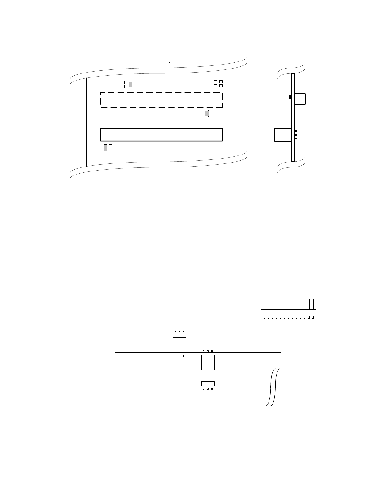
Lubbock Platform
The Lubbock platform has a single 140-pin connector, J26 that interfaces to the adapter board (described
earlier) that re-routes several signals necessary to work with the Evaluation board. The final assembly
should resemble the diagram below which is a side view of the Lubbock platform and Evaluation Board.
MQ-1168 Evaluation
Board, Veiw From Side
MQ-1132/1168 SA-1110 &
PXA2x0 Adapter Board
PXA2X0 (Lubbock) Platform
The MQ1168 peripherals with the exception of the flatpanel interface need to signal the PXA2x0 on the
Lubbock platform with an interrupt. Our device drivers have been ported to use GPIO 10/RTC on the
Lubbock connector as the interrupt pin.GPIO 10 comes out on connector J21 pin 3 as defined in the
Lubbock user guide on page 2-13. If you intend to use GPIO 10 you need to solder a wire from the
MQ1168 interface card connector U2 pin 108 to Connector J21 pin 3. Other interrupt pins can be used by
connecting them to Pin 108 of connector U2 on the interface card, however the drivers will need to be
modified.
Assabet Platform
The diagram below shows how the Evaluation board, adapter board and Assabet platform are connected.
Care should be taken to line up the pins correctly, especially A1/B1/C1. Also, when removing the adapter
from the Assabet platform, care should be taken to ensure the boards come apart as parallel as possible or
the pins on the male adapter board connector can be bent or the plastic shroud broken.
SA-1110
Assabet
SA-Adapter for
MQ1132/MQ-1168
Used with MQ-
1132 board only
MQ-1168 Evaluation
Board, Veiw From Side

MQ-1168 Evaluation Board Users Guide MediaQ Incorporated
Board Revision 2
Revision A 4/18/02 Preliminary 9
Care should be taken to ensure correct alignment of the sockets and plugs to prevent damage during
assembly and disassembly. When removing either the Evaluation or Adapter Board from the platform,
apply even pressure is to both sides of the connector and keep the boards as parallel as possible to prevent
damage to the Plug pins and moldings.
Lubbock Platform Configuration & Operation
Consult the documentation listed below relating to the Lubbock platform for instructions on how to
configure and bring up that system.
SA-1110 (Assabet) Platform Configuration & Operation
The following instructions apply to using the Evaluation Board with the Intel StrongARM SA-1110
Reference Platform. The following components are required and should be included in the Intel
SA1110/SA1111 development package:
§SA-1110 platform module (Assabet)
§SA-1111 developer platform module (Neponset)
§DC supply for platform
§Compact flash Ethernet card, CF to PCMCIA adapter and crossover cable
§Serial cable (10-pin female header to 9-pin female serial port connector)
Please note that no compact flash adaptor should be installed in the SA1110 board socket, as it will cause
damage to the card and the bus drivers used to drive the MQ-1168 & SA1111 board’s bus.
Software Download
After the hardware is assembled, connect the serial and ethernet connectors to a properly configured host
PC. The configuration of the host is beyond the scope of this document and should be covered in the
StrongARM documentation. Following are the steps required to download a software image to the
platform system memory.
1. Open a hyper-terminal on the host PC. The communication setting for Eboot is provided in the
Intel document “Intel StrongARM SA-1110 Microprocessor Development Board Users Guide”
2. Open the Eshell on the host PC for Window CE shell
3. Power on the system and the hyper-terminal should print some messages and stop at the point
“Init DHCP()”
4. Input an IP address here with the first three areas the same as your host PC setting (for example, if
your host PC IP address setting is 192.168.1.128, you need an IP address 192.168.1.x. The
network mask may not need to be set in which case, just press return and it will be set
255.255.255.x. Otherwise set the mask to 255.255.255.0. Hyper-terminal will print “SENT
BOOTME TO 255.255.255.x.)
5. In Eshell window, select the SA-1110 device as controller device in option and set configuration
“download only on command, unselect all other option”. If setup is correct, it will print out
“Got Bootme from SA11xxxxxx, ready for download”.
6. Select the desired binary file and proceed with download. It will display download status at the
bottom left corner of the Eshell window.
7. After download, the system will reboot and execute the image file. For program information, refer
to the Intel documentation.

MQ-1168 Evaluation Board Users Guide MediaQ Incorporated
Board Revision 2
Revision A 4/18/02 Preliminary 10
Following are the steps required to download a software image to the platform flash memory.
1. Download the Flash Memory Programmer (JFlash), version 1.2 from
http://developer.intel.com/design/strong/swsup/
2. Unzip and read the readme.doc to setup the JFlash application. Run “jfsetup.bat.”
3. Note: Requires Intel Jtag cable. ( P/N 70-11131-12 REV 2.1 044)
4. Download “Ebootdwv5.nb0” from ftp://ftp.mediaq.com/sw/mq11xx/windowsce/utils/jflash/
5. To Download image into the Neponset (SA1111) set dip switch 1, 2, 7 ON of the “SW2.”
6. To Download image into the Assabet (SA1110) set dip switch 1, 2, 7, & 8ON of the “SW2.”
7. Once “Ebootdwv3.nb0” is flashed into the platform, select “Ethernet loader without launch” to
download image onto flash. Follow the steps required to download a software image to the
platform system memory.
8. Once image download is done, select “Program to flash” from the hyper terminal to copy image
into flash memory.
9. After program to flash is complete, perform cold boot.

MQ-1168 Evaluation Board Users Guide MediaQ Incorporated
Board Revision 2
Revision A 4/18/02 Preliminary 11
Palm & Motorola Dragonball Platform (Hurricane & ) Adapter
A1
B1
C1
A1
B1
C1
A1
B1
C1
J2
U4
U6
U5
J1
JP1
The diagram above shows the adapter for the Palm Development Platform (Hurricane) or the Motorola
Development Platform. As with the other adapters, J2 mates with the “Generic CPU” connector located
on the back of the Evaluation board. Connector U4 mates with the 96-pin female DIN connector on the
Palm Hurricane Platform. Alternately, connector U6 can be used to connect to the Motorola
Development Platform. These connectors are keyed so cannot be installed incorrectly. J1 selects which
IRQ the MQ-1168 will connect to on the platform. Setting 1-2 selects IRQ2 while 2-3 selects IRQ3. The
Evaluation board requires 3.3V and 5V power from the adapter board. The Palm/Motorola adapter passes
the 3.3V power supplied on the platform connector but does not provide 5V. Connector JP1 is used to
provide 5V and can be connected to an external source. A wire with a mating female 0.25” square
connector can be attached to the 5V supply which does not go to the bus but is available on the platform.
The diagram below shows how the Evaluation board, adapter board and Palm or Mororola platforms are
connected. Care should be taken to line up the pins correctly, especially A1/B1/C1.
Palm Hurricane
Platform
MQ-1168 Evaluation
Board, Veiw From Side
Palm/Motorola Adapter
for MQ-1168
Motorola Platform

MQ-1168 Evaluation Board Users Guide MediaQ Incorporated
Board Revision 2
Revision A 4/18/02 Preliminary 12
NEC VR4121 Platform (Falcon) Adapter
FALCON CONNECTOR-
MALE
A1
B1
C1
D1
C1
B1
A1
D1
C1
B1
A1
B1
A1
J4
J2
J3
J6
The diagram above shows the adapter for the NEC VR4121 Development Platform (Falcon). J6 mates
with the “Generic CPU” connector located on the back of the Evaluation board. Male 2mm pitch headers
J2, J3 and J4 mate with matching connectors on the NEC Falcon Platform. These connectors are not
keyed and care should be exercised to line up the pins correctly. When removing the adapter from the
platform, be very careful not to bend the pins. The diagram below shows how the Evaluation board, NEC
Falcon adapter and NEC Falcon platform are connected.
NEC VR4121
Falcon Platform
MQ-1168 Evaluation
Board, Veiw From Side
NEC Falcon Adapter
for MQ-1168
MQ-1168 Evaluation Board Users Guide MediaQ Incorporated
Board Revision 2
Revision A 4/18/02 Preliminary 13
Hitachi SH7709/7750 Platform (S1/R1) Adapter
A1
B1
C1
1
51
151
101
50
150
100
200
J2
J1
R10
R9
R11
R3
R8
0
10K
10K
R2
R1
R4
R5
10K
The adapter for the Hitachi 7709/7750 based Development Platforms (S1/R1) is shown above. J2 mates
with the “Generic CPU” connector located on the back of the Evaluation board. The Male 0.05” pitch
connector J1 mates with the matching connector on the Hitachi platforms. This connector is not keyed
and care should be exercised so as not to plug the adapter in backwards. When removing the adapter from
the platform, be very careful not to bend the pins. The adapter can be configured to work with either the
Hitachi SH7709 or SH7750 CPUs. For the SH7709 also known as the SH3 processor, R1 (10K ohm
resistor) and R4 (0 ohm resistor) should be installed. For the SH7750 also known as the SH4 processor,
R2 (10K ohm) and R5 (0 ohm) should be installed instead. These changes set the MQ1168 CPU mode
select and pull the RDY#/WAIT# line in the correct direction. Resistors R8, R9, R10 and R11 can be
removed to isolate three of the power/ground pins and the interrupt pin for use on some platforms that
were not completely pin compatible with the standard S1 connector. The diagram below shows how the
Evaluation board, Hitachi 7709/7750 adapter and Hitachi platform are assembled.
Hitachi S1/R1
Platform
MQ-1168 Evaluation
Board, Veiw From Side
Hitachi 7709/7750
Adapter for MQ-1168

MQ-1168 Evaluation Board Users Guide MediaQ Incorporated
Board Revision 2
Revision A 4/18/02 Preliminary 14
RELATED DOCUMENTATION
• MQ-1168 Multimedia Platform Controller Datasheet
• Flat Panel Support Application Note
• MediaQ Software release notes
• Intel® StrongARM® SA-1110 Microprocessor Developers Manual (278240-003)
• Intel® StrongARM® SA-1110 Microprocessor Development Board User’s Guide (278278-005)
• Intel® StrongARM® SA-1110/SA-1111 Development Kit Start Proceedures User’s Guide
(278339-002)
• Intel® StrongARM® SA-1110 Microprocessor Development Board Schematics (278279-006)
• Intel® PXA250/PXA210 Applications Processor Developers Manual (278522-001)
• Intel® DBPXA250 Development Platform for Intel ® PCA Quick Start Guide (278403-001)
• Intel® DBPXA250 Development Platform for Intel ® PCA User’s Guide (278419-001)
• Intel® BBPXA2XX Development Baseboard Schematic Diagram (278424-001)
* Intel® and XScaleT are trademarks of Intel Corporation

5
5
4
4
3
3
2
2
1
1
D D
C C
B B
A A
MQ-T2
DNS
DNS
DNS DNS
1 2MQ-1168 Evaluation DesignB
111Tuesday, April 16, 2002
Title
Size Document Number Rev
Date: Sheet of
FP_B[5..0]
FP_B4
FLCLK
FP_ENVEE
FP_B5
FP_B3
FP_B1
FP_B0
FP_B2
FP_ENVDD
FP_R4
FP_R[5..0]
FP_G2
FP_R3
FP_R2
FP_G3
FP_R1
FP_G1
FP_G[5..0]
FP_G0
FP_R0
FP_G5
FP_G4
FP_R5
SDCMD_G65
SDCLK_G64
SDD1_G61
SDD0_G60
AD6
AD13
AD17
AD2
AD4
AD20
AD29
AD9
AD14
AD8
DEVSEL_N
AD23
AD28 AD10
AD[31..0]
AD27
AD3
VINCLK_G78
AD22
AD1
AD18
AD19
AD21
AD24
AD25
AD26
AD11
AD7
AD15
AD12
AD16
AD30
AD5
VID4
TP_CS_G50
CLK_SPI_G51
AD31
FP_PWM0
FVSYNC
FP_DESPL
USB1_DN
USB0_DP
FP_LP
VID6VID8
VID3
VID0
DATAIN_SPI_G53
SDD2_G62
DATAOUT_SPI_G52
FP_PWM1
VID7
VID2
SDD3_G63
USB0_DN
FMOD
FP_SCLK
VID1
VID[0..7]
VID5
USB1_DP
AD0
CBE1_N
CLK
TRDY_N
FRAME_N
MQ_IRL_N
AUDIO_MD_G3
AUDIO_MC_G0
IDSEL_G22
IRDY_N
CBE3_N_G21
PAR
SERR_N_G23
QMUTE_G40
VHSYNC_G79
SD_COM_G25
SD_DETECT_G1
VVSYNC_G80
FP_MODE_G5
STOP_N
CBE0_N
PERR_N_G24
AUDIO_ML_G4
CBE2_N_G20
POR_N
PENIRQ_G2
AUDIO_DOUT_G44
AUDIO_BCLK_G42
AUDIO_DIN_G45
AUDIO_L_R_G43
AUDIO_SYSCLK_G41
G54
SDLOW
FP_G[5..0] 4,5
FP_B[5..0] 4,5
FP_SCLK 4,5
VID[0..7]8
AD[31..0]2
FLCLK 4,5
FP_DESPL 4,5
FP_PWM1 4,5
FP_ENVEE 3,5
FMOD 3,5
FVSYNC 4,5
FP_PWM0 5
FP_LP 4,5
FP_ENVDD 3,5
CBE3_N_G212
FRAME_N2PAR2
CBE0_N2
IDSEL_G222
CBE2_N_G202 CBE1_N2
PERR_N_G242
DEVSEL_N2
SERR_N_G232
STOP_N2
CLK2
PENIRQ_G210
SD_DETECT_G12,10
TRDY_N2IRDY_N2
MQ_IRL_N2
SDD2_G62 10
SDD1_G61 10
DATAOUT_SPI_G52 10
SDCLK_G64 10
SDD0_G60 10
FP_R[5..0] 4,5
DATAIN_SPI_G53 10
SDD3_G63 10
TP_CS_G50 10
SDCMD_G65 10
CLK_SPI_G51 10
QMUTE_G406
AUDIO_MD_G36
VHSYNC_G798VINCLK_G788
VVSYNC_G808
G54_G24 2,10
AUDIO_MC_G02,6
SD_COM_G252
POR_N2,6,7,8
FP_MODE_G52,4,5
USB0_DP 11
USB1_DP 11
USB1_DN 11
USB0_DN 11
AUDIO_ML_G46
AUDIO_SYSCLK_G416AUDIO_BCLK_G426,7
AUDIO_DIN_G456,7
AUDIO_L_R_G436,7 AUDIO_DOUT_G446,7
SDLOW 2
CVDDBVDD FVDD
AVDD18
MVDD USBVDDAVDDP18
3.3VBUS
R116
1M
J6 12
HOST BUS INTERFACE
FLAT PANEL INTERFACE
CODEC/I2S
HOST BUS
T2-6/6/01
VIDEO INPUT
POWER & GND
RESET,MODE CONTROL
SPI
SECURE DIGITAL
U28
K8
G12
H10
H11
J11
J10
K12
J12
K11
L12
K10
M12
L11
M11
L10
M10
M9
B1
A1
D3
B4
C3
C4
A2
C2
L8
M7
L9
L7
L6
L5
K5
L4
K4
M3
L3
M2
L2
M1
L1
K3
K2
J1
J3
J2
H3
H2
B2
C9
C10
B10
A11
C11
B11
C7
A8
C8
B8
B9
A9
B5
C5
A6
B6
C6
B7
B3
E12
D12
A12
B12
H9
G9
F9
E9
D11
D9
G3
J7
J8
J9
F1
G1
D10
E8
E6
H5
G5
F5
E5
K6
K9
K7
G4
F4
E4
D4
D5
D6
D7
D8
H4
J4
J5
H1
A5
H12
M6
C1
M5
A4
F12
M4
K1
G8
H6
G6
A3
A10
M8
F6
F8
D1
A7
E7
C12
J6
E3
F3
F2
G2
E2
D2
E1
E11
E10
F11
G11
F10
G10
F7
H7
H8
G7
I_CS_N
B_D0
B_D1
B_D2
B_D3
B_D4
B_D5
B_D6
B_D7
B_D8
B_D9
B_D10
B_D11
B_D12
B_D13
B_D14
B_D15
O_EN_VDD_GPIO
O_EN_VEE_GPIO
O_FDE_FSSP_GPIO
O_VSYNC_FGSP_FLM_GPIO
O_HSYNC_FLP_GPIO
O_FSCLK
O_PWM0_GPIO
O_PWM1_FLCLKA_GPIO
I_WE0_N
I_WE1_N
I_RD/WR_N
O_RDY_N
I_A1
I_A2
I_A3
I_A4
I_A5
I_A6
I_A7
I_A8
I_A9
I_A10
I_A11
I_A12
I_A13
I_A14
I_A15
I_A16
I_A17
I_A18
O_FMOD_GPIO
O_FD18
O_FD19
O_FD20
O_FD21
O_FD22
O_FD23
O_FD10
O_FD11
O_FD12
O_FD13
O_FD14
O_FD15
O_FD2
O_FD3
O_FD4
O_FD5
O_FD6
O_FD7
O_FLCLK_GPIO
B_USB1_D
B_USB1_D_N
B_USB2_D_N
B_USB2_D
I_SRCLK_GPIO40
O_SMCLK_GPIO41
O_SCLK_GPIO42
O_FSYNC_GPIO43
O_SOUT_GPIO45
I_SIN_GPIO44
B_LED_GPIO54
B_SPICLK_GPIO51
B_MOSI_GPIO52
B_MISO_GPIO53
OSCI
OSCO
I_POR_N
PCIMDN_GPIO5
B_GPIO4_PDWN_N
I_MD0_GPIO0
I_MD1_GPIO1
I_MD2_GPIO2
I_MD3_GPIO3
I_CKIO
O_IRL_N
I_BS_N
VID0_GPIO70
VID1_GPIO71
VID2_GPIO72
VID3_GPIO73
VID4_GPIO74
VID5_GPIO75
VID6_GPIO76
VID7_GPIO77
VINCLK_GPIO78
VHSYNC_GPIO79
VVSYNC_GPIO80
MVDD2
AVDDP2
MVDD1
AVDDP1
AGND18
AGNDP1
AGNDP2
BVDD1
BVDD2
BVDD3
BGND1
BGND2
BGND3
FVDD1
FVDD2
CVDD2
FGND1
FGND2
AVDD18
CVDD1
PGND
PVDD
B_SSN_GPIO50
B_SDD3_GPIO63
B_SDD2_GPIO62
B_SDD1_GPIO61
B_SDD0_GPIO60
B_SDCLK_GPIO64
B_SDCMD_GPIO65
OSCR
CBE2_N_GPIO20
CBE3_N_GPIO21
IDSEL_GPIO22
SERR_N_GPIO23
PERR_N_GPIO24
CLKRUN_N_GPIO25
CGND1
CGND2
MGND1
MGND2
J10
CON3
1
2
3
R27
100
R119
0C108 33pF
R118 0
OSC1
EPSON SG-636PCV 48.000MCQ
4
2 1
3
vdd
gnd en/st
clk
R111 100K
D2
LED GREEN
Y3
3.684Mhz
R109 100K
J8
1
2
3
R75
100K
C121 33pF
R114
180K1%

5
5
4
4
3
3
2
2
1
1
D D
C C
B B
A A
PCI Interface and Generic CPU interface
THE STARPPING FOR DIFFERENT CPU IS DONE ON THE ADAPTER CARD BASED ON THIS TABLE
00
1
1
MC
0
1
01 1
TX
10
PCI
01
X 1
GENERIC CPU CONNECTOR
SH3
MD[1:0] BS_N CKIO PCIMDN MODE
0
X
1
X
X
1
VR
X
1
X
XX
00
SA
SH4
0
11
1
X
X
X
1 0 7 6 5
p# 929647-04-36-ND(single row)
p# 929665-03-36-ND(dual row)
1 2MQ-1168 Evaluation DesignB
211Tuesday, April 16, 2002
Title
Size Document Number Rev
Date: Sheet of
IDSEL_G22
AD10
AD25
AUDIO_MC_G0
CLK
FP_MODE_G5
CBE3_N_G21
AD18
SERR_N_G23
AD20
COM_SD
SD_COM_G25
CBE0_N
AD6
AD9
AD11
TRDY_N
SD_DET_G1
FRAME_N
DEVSEL_N
AD22
PERR_N_G24
STOP_N
FP_MODE_G5
AD2
FRAME_N
CBE3_N_G21
CBE0_N
IRDY_N
SD_DETECT_G1
AD16
CBE2_N_G20
CBE2_N_G20
PAR
AD27
AUDIO_MC_G0
AD7
SERR_N_G23
AD21
SD_DETECT_G1
CBE2_N_G20
AD3
AD12
CBE1_N
AD30
PCISEL_N
MQ_IRL_N
CBE1_N
AD31
DEVSEL_N
AD4
STOP_N
CBE0_N
TRDY_N
POR_N
MQ_IRL_N
CLK
AD0
AD29
CLK
SD_COM_G25
USB_G23
COM_SD
AD15
AD8
AD17
PERR_N_G24
G54_G24
AD23
AD1
AD24
IRDY_N
POR_N
AD13
AD5
AD26
AD19
AD28
USB_G23
PAR
AD14
PAR
AUDIO_MC_G0
SDLOW
SDLOW
CBE3_N_G21
SD_DET_G1
MQ_IRL_N
TRDY_N
CBE1_N
DEVSEL_N
COM_SD
IRDY_N
POR_N
SERR_N_G23
PERR_N_G24
PCISEL_N
IDSEL_G22
STOP_N
PAR
FRAME_N
AD1
USB_G23
AD0
AD31
AD24
AD4
AD9
AD12
AD28
AD21
AD17
AD11
AD27
AD16
AD8
AD22
AD14
AD5
AD25
AD18
AD6
AD29
AD7
AD30
AD20
AD19
AD2
AD26
AD3
AD10
AD15
AD23
AD13
G54_G24
CBE3_N_G211
AUDIO_MC_G01,6
CLK1
SD_DETECT_G11,10
MQ_IRL_N1
CBE2_N_G201
PAR1
PERR_N_G241
STOP_N1
CBE0_N1
IRDY_N1
FRAME_N1
TRDY_N1
AD[31..0] 1
FP_MODE_G51,4,5
CBE1_N1
SERR_N_G231
IDSEL_G221
POR_N1,6,7,8
DEVSEL_N1
COM_SD10
SD_COM_G251
USB_G2311
SDLOW1
G54_G241,10
3.3VBUS
3.3VBUS
5VBUS
3.3VBUS3.3VBUS
5VBUS
R121 100K
R94
100K
R93 100K
C69
0.01uf
R95 100K
C72
0.01uf
C73
0.01uf
R122 100K
C71
0.01uf
C75
0.01uf
J11
pci_univ
1a
2a
3a
4a
5a
6a
7a
8a
9a
10a
11a
14a
15a
16a
17a
18a
19a
20a
21a
22a
23a
24a
25a
26a
27a
28a
29a
30a
31a
32a
33a
34a
35a
36a
37a
38a
39a
40a
41a
42a
43a
44a
45a
46a
47a
48a
49a
52a
53a
54a
55a
56a
57a
58a
59a
60a
61a
62a
1b
2b
3b
4b
5b
6b
7b
8b
9b
10b
11b
14b
15b
16b
17b
18b
19b
20b
21b
22b
23b
24b
25b
26b
27b
28b
29b
30b
31b
32b
33b
34b
35b
36b
37b
38b
39b
40b
41b
42b
43b
44b
45b
46b
47b
48b
49b
52b
53b
54b
55b
56b
57b
58b
59b
60b
61b
62b
trst_n
+12v
tms
tdi
+5v
inta_n
intc_n
+5v
res
vio
res
3.3vaux
rst_n
vio
gnt_n
gnd
pme_n
ad30
+3.3 v
ad28
ad26
gnd
ad24
idsel
+3.3v
ad22
ad20
gnd
ad18
ad16
+3.3v
frame_n
gnd
trdy_n
gnd
stop_n
+3.3v
res
res
gnd
par
ad15
+3.3v
ad13
ad11
gnd
ad9
c/be0_n
+3.3v
ad6
ad4
gnd
ad2
ad0
vio
req64_n
+5v
+5v
-12v
tck
gnd
tdo
+5v
+5v
intb_n
intd_n
prsnt1_n
res
prsnt2_n
res
gnd
clk
gnd
req_n
vio
ad31
ad29
gnd
ad27
ad25
+3.3v
c/be3_n
ad23
gnd
ad21
ad19
+3.3v
ad17
c/be2_n
gnd
irdy_n
+3.3v
devseln
gnd
lock_n
perr_n
+3.3v
serr_n
+3.3v
c/be1_n
ad14
gnd
ad12
ad10
m66en
ad8
ad7
+3.3v
ad5
ad3
gnd
ad1
vio
ack64_n
+5v
+5v
J2-B1
1
2
3
4
5
6
7
8
9
10
11
12
13
14
15
16
17
18
19
20
21
22
23
24
25
+
C74
47uF10V
J2-C1
1
2
3
4
5
6
7
8
9
10
11
12
13
14
15
16
17
18
19
20
21
22
23
24
25
+
C76
47uF10V
C70
0.01uf
J2-A1
1
2
3
4
5
6
7
8
9
10
11
12
13
14
15
16
17
18
19
20
21
22
23
24
25

5
5
4
4
3
3
2
2
1
1
D D
C C
B B
A A
HR TFT FLAT PANEL INTERFACE PAGE 1
HR-TFT interface #1
1 2
MQ-1168 Evaluation Design
B
311Tuesday, April 16, 2002
Title
Size Document Number Rev
Date: Sheet of
V0
V9
V2
V7
V4
V5
V6
V1
V8
V3
V[9..0]
VCOM_AC_DC
VEE_AC_DC
FMOD
POWER POWER
POWER
V[9..0] 4
FMOD 1,5
VCOM_AC_DC 4
VEE_AC_DC 4
FP_ENVDD1,5
FP_ENVEE1,5
-15V
5VBUS 3.3VBUS
3.3V
5V
+15V -15V -11.7V
5VBUS5V
U21
Micrel MIC2570-2 1
2
3
45
6
7
8SW
GND
NC
NCNC
IN_FB
IN_SYNC
IN
C79
4.7uF
R42 100K
C20
1uF
R49
12K
R45
22K
+
C27
22uF16V
C29
2.2uF CERAMIC
D6
1N4148
+
C94
100uF10V
R37
14K
Q1
2SC1815
3
1 2
D5
1N4148
U20
SI9953DY
4 5
6
1
2
37
8
G2 D2
D2
S1
G1
S2 D1
D1
+
C39
22uF16V
R35
1M
R48
20
U22
Micrel MIC2570-2 1
2
3
45
6
7
8SW
GND
NC
NCNC
IN_FB
IN_SYNC
IN
C32
0.1uF
R32 0
C97
0.1uF
C24
0.1uF
Q2
2SA1161
1
23
C28
0.1uF
U23A
74LS04
1 2
R40
15K
R41
47K
R26
240
C25
0.01uF
U19
LM337LM SO-8
1
2
3
4
8
7
6
5
Vout
Vin
Vin
ADJ
NC
Vin
Vin
NC
L2 47uH, Coilcraft DO3316P-473
R36
1M
U5
IR3E204N-SHARP
1
2
3
4
5
6
7
8
9
18
17
16
15
14
13
12
11
10
NC
VDD
VCC
COM
V0
V1
V2
V3
V4
NC
NC
SW
V9
V8
V7
V6
V5
GND
R50
120K
L1 47uH, Coilcraft DO3316P-473
R39
220K
C36
0.1uF
D7
MBRA140T3
D3
MBRA140T3
2 1
R29
2K
U26
MMDF2C02E
4 5
6
1
2
37
8
G2 D2
D2
S1
G1
S2 D1
D1
R34
16K
+
C95
100uF10V
D4 MBRA140T3
R46
20
+
C30
33uF20V
+
C33
22uF16V
+
C41
22uF16V
R47 33K
C31
0.1uF
D8
R31 0
U23C
74LS04
5 6
C23
0.1uF
R38 100K
U23B
74LS04
3 4

5
5
4
4
3
3
2
2
1
1
D D
C C
B B
A A
HR TFT FLAT PANEL INTERFACE PAGE 2
SHARP HR TFT INTERFACE
HR-TFT interface #2
<Doc> 2MQ-1168 Evaluation DesignB
411Tuesday, April 16, 2002
Title
Size Document Number Rev
Date: Sheet of
FP_G5
FP_G2
FP_B1
FP_R4
V3
FP_R2
FP_G0
FP_R1
FP_G[5..0]
V4
V[9..0]
FP_B3
FP_R5
V8
FP_HSCAN_DIR
FP_G4
FP_VSCAN_DIR
FP_DESPL
FP_B5
VEE_AC_DC
FP_R0
FP_B[5..0]
FP_B4
FP_PWM1
V7
FP_B2
FVSYNC
V6
FP_R3
FP_B0
V5
FP_LP
FP_G3
FP_R[5..0]
V0
VCOM_AC_DC
V2
FLCLK
V1
FP_MODE
FP_G1
FP_SCLK
V9
FP_PWM1 1,5
FVSYNC 1,5
FLCLK 1,5
FP_SCLK 1,5
FP_DESPL 1,5
FP_R[5..0] 1,5
FP_G[5..0] 1,5
FP_B[5..0] 1,5
V[9..0] 3
VEE_AC_DC 3
VCOM_AC_DC 3
FP_LP 1,5
FP_MODE_G5 1,2,5
+15V 3.3V-11.7V -15V5V
3.3V 3.3VBUS
R6
0
U1
FCON50
1
2
3
4
5
6
7
8
9
10
11
12
13
14
15
16
17
18
19
20
21
22
23
24
25
26
27
28
29
30
31
32
33
34
35
36
37
38
39
40
41
42
43
44
45
46
47
48
49
50
1
2
3
4
5
6
7
8
9
10
11
12
13
14
15
16
17
18
19
20
21
22
23
24
25
26
27
28
29
30
31
32
33
34
35
36
37
38
39
40
41
42
43
44
45
46
47
48
49
50
R3
10K
R7
0
R2
10K

5
5
4
4
3
3
2
2
1
1
D D
C C
B B
A A
GENERIC FLAT PANEL INTERFACE
GENERIC FLAT PANEL INTERFACE
CONTRAST ADJUSTMENT
PULSE WIDTH MODULATION
Generic Flat panel interface
TEST HEADER
<Doc> 2MQ-1168 Evaluation DesignB
511Tuesday, April 16, 2002
Title
Size Document Number Rev
Date: Sheet of
FP_PWM0
FP_MODE_G5
FP_PWM1
FMOD
FP_SCLK
PWMCON0
FLCLK
FP_DESPL
FP_DESPL
FP_B[5..0]
FP_LP
FP_LP
FP_B1
FP_G3
FP_R5
FP_R1
FP_R3 FP_B2
FP_G4
FP_G0 FMOD
FP_R3
FP_R0
FP_G5
FP_B5
FP_G1
FP_B2
FP_MODE_G5 FP_ENVDD
FP_R0
FP_SCLK
FP_G4
FP_B3
FVSYNC
FP_G0
FP_DESPL
FVSYNC
FP_B5
FP_B4
FVSYNC
FP_G2
FP_R1
FP_B0
FP_G2
FP_G3
FP_R5
PWMCON0
FP_PWM1
FP_R2 FP_B4
FP_B0
FP_R4 FLCLK
FP_G[5..0]
FP_R[5..0]
FP_R2
FP_G1 FP_LP
FP_B3
PWMCON0
FP_R4
FP_B1
FP_G5
FP_ENVDD
FP_ENVEEFP_ENVEE
FP_ENVEE
FP_PWM01
FVSYNC1,4
FP_B[5..0]1,4
FLCLK1,4
FP_SCLK1,4
FP_PWM11,4
FP_R[5..0]1,4
FMOD1,3
FP_MODE_G51,2,4
FP_G[5..0]1,4
FP_ENVEE1,3
FP_DESPL1,4
FP_LP1,4
FP_ENVDD1,3
+15V 5V-15V
3.3VBUS
-11.7V
3.3V 3.3V5V-11.7V-15V+15V
U6
1
J5
HDR 2X30, 0.1
2
4
6
8
10
12
14
16
18
20
22
24
26
28
30
32
34
36
38
40
42
44
46
48
50
52
54
56
58
60
1
3
5
7
9
11
13
15
17
19
21
23
25
27
29
31
33
35
37
39
41
43
45
47
49
51
53
55
57
59
U14
1
U7
1
R5
100 K
U8
1
U15
1
C1NI
R97
100 K
U9
1
+
C19
47uF10V
R4
100 K
+
-
U2A
LM358N
3
21
84
J3
HDR 2X30, 50 Mils
2
4
6
8
10
12
14
16
18
20
22
24
26
28
30
32
34
36
38
40
42
44
46
48
50
52
54
56
58
60
1
3
5
7
9
11
13
15
17
19
21
23
25
27
29
31
33
35
37
39
41
43
45
47
49
51
53
55
57
59
U10
1
R1
100 K
R96
510 K
+
C14
47uF10V
U12
1
C77
0.1uF

5
5
4
4
3
3
2
2
1
1
D D
C C
B B
A A
AUDIO
Audio DECODER
1 2MQ-1168 Evaluation DesignB
611Tuesday, April 16, 2002
Title
Size Document Number Rev
Date: Sheet of
AUDIO_BCLK_G42
AUDIO_MC_G0
AUDIO_MD_G3
AUDIO_DOUT_G44
AUDIO_DOUT_G44
AUDIO_MD_G3
AUDIO_ML_G4
AUDIO_BCLK_G42
QMUTE_G40
QMUTE_G40
POR_N
AUDIO_MC_G0
AUDIO_SYSCLK_G41
AUDIO_ML_G4
AUDIO_SYSCLK_G41
AUDIO_L_R_G43
AUDIO_DIN_G45
AUDIO_L_R_G43
AUDIO_DIN_G45
AUDOUL 7
AUDIO_DOUT_G441,7
AUDIO_DIN_G451,7
AUDIO_BCLK_G421,7
AUDIO_SYSCLK_G411
SHAREMIC7
POR_N1,2,7,8
AUDIO_MC_G01,2
AUDIO_L_R_G431,7
AUDINL7
AUDIO_ML_G41
AUDOUR 7
QMUTE_G401
AUDINR7
AUDIO_MD_G31
3.3AV
3.3VBUS5VBUS
R65 0
C99
0.1uF
R60 0
R43
0
R110 0
+
C34 47uF10V
U24
1
R115
0
R58 0
+
C38 47uF10V
C102
0.1uF
R55
10k
R53 0
R68 0
+
C107 47uF10V
C101
0.1uF
UDA1341TS
U27
6
8
2
13
4
22
14
18
15
9
24
26
23
25
28
7
3
16
17
19
12
5
110
27
11
21
20
VINL2
VINR2
VINL1L
L3MODE
VINR1L
AGCSTAT
L3CLOCK
DATAO
L3DATA
OVERFL
VOUTR
VOUTL
QMUTE
VDDA
Vref
VADCP
VDDA
BCK
WS
DATAI
SYSCLK
VADCN
VSSA VDDD
VSSA
VSSD
TEST2
TEST1
+
C43
220uF16V
+
C42 47uF10V
R113 0
R44 0
R54
0
U25
1
R71 0
+
C100 47uF10V
R63
10k
J9
HEADER 10X2(.1 SPACING)
1
3
5
7
9
11
13
15
17
19
2
4
6
8
10
12
14
16
18
20
CN3
PHONEJACK
3
2
1
+
C35
47uF10V
+
C110
220uF16V
R57 0
R52 0
R73
0
R66 0
R72
0
R62 0
C98
0.1uF
+
C40 47uF10V
+
C96
220uF16VCN4
PHONEJACK
3
2
1
R112 0
C37
0.1uF
R51
0
Table of contents
Other MediaQ Motherboard manuals


