Moog Norlin 204D User manual

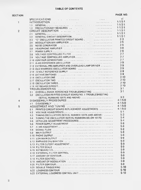
TABLE
OF
CONTENTS
SPECIFICATIONS
.
1
INTRODUCTION
.
1.1
GENERAL.
1.2
PRECAUTIONARY
MEASURES
.
2
CIRCUIT
DESCRIPTION
.
2.1
GENERAL.
2.2
GENERAL
CIRCUIT
DESCRIPTION.
2.3
"D"
OSCILLATOR
PRINTED
CIRCUIT
BOARD.
2.4
MODULATION
MIX
AMPLIFIER.
2.5
NOISE
GENERATOR.
2.6
HEADPHONE
AMPLIFIER
.
2.7
POWER
SUPPLY.
2.8
VOLTAGE
CONTROLLED
FILTER
.
2.9
VOLTAGE
CONTROLLED
AMPLIFIER.
2.10
CONTOUR
GENERATORS
.
2.11
A-440
REFERENCE
OSCILLATOR
.
2.12
EXTERNAL
PREAMPLIFIER
AND
OVERLOAD
LAMP
DRIVER.
2.13
OLD
MINIMOOG
OSCILLATOR
BOARD
.
2.14
-5
VOLT
REFERENCE
SUPPLY
.
2.15
OCTAVE
SWITCHES
.
2.16
OSCILLATOR
ONE
.
2.17
OSCILLATOR
TWO
.
2.18
OSCILLATOR
THREE.
2.19
KEYBOARD
CIRCUIT..
3
TROUBLESHOOTING
.
3
1
OVERALL
QUICK
REFERENCE
TROUBLESHOOTING
.
3.2
O
SCILLATOR
PRINTED
CIRCUIT
BOARD
NO.
1
TROUBLESHOOTING
(SERIAL
NUMBERS
10176
AND
ABOVE).
4
DISASSEMBLY
PROCEDURES.
41
DISASSEMBLY
.
5
ADJUSTMENT
AND
TUNING
.
5.1
PRINTED
CIRCUIT
BOARD
REPLACEMENT
ADJUSTMENTS.
5.2
VOLTAGE
ADJUSTMENTS.
5.3
TUNING
OSCILLATORS
(SERIAL
NUMBER
10175
AND
ABOVE)
.
.
5.4
TUNING
THE
OSCILLATOR
(SERIAL
NUMBERS
8ELOW
10175)
.
.
.
5.5
DETAILED
ADJUSTMENT
PROCEDURES.
5.6
POWER
SUPPLY
ADJUSTMENT
.
5.7
A-440
ADJUSTMENT.
5.8
SIGNAL
FLOW
.
5.9
MAIN
OUTPUT
.
5.10
PHONE
OUTPUT.
5.11
LOW
MAIN
OUTPUT
.
5.12
EMPHASIS
CALIBRATION.
5.13
FILTER
CUTOFF
ADJUSTMENT.
5.14
FILTER
SCALE.
5.15
KEYBOARD
1/3.
5.16
EXTERNAL
FILTER
CONTROL
.
5.17
AMOUNT
OF
CONTOUR
.
.
.
5.18
FILTER
CONTROL.
5
19
AMOUNT
OF
MODULATION
.
5.20
FILTER
CONTOUR.
5.21
DOUBLE
TRIGGERING
.
5.22
LOUDNESS
CONTOUR
.
5.23
EXTERNAL
LOUDNESS
CONTROL
UNIT.
PAGE
NO.
11
/
2-1
11/2-1
1
-1/2-1
11/2-1
11/2-1
11/2-1
2-3
2-5
2-5
2-6
2-6
2-7
2-7
2-7
2-9
2-9
2-9
2-9
2-
9
2-10
2-10
2
10
2-10
3-
1
3-1
3-3
4-1/5-0
4-1/5-0
4-1/5-0
4
1/5-0
5-1
5-3
5-4
5-4
5-8
5-8
5-8
5-8
5-8
5-9
5-9
5-9
5-9
5-9
5-9
5-9
5-9
5-9
5-9
5-10
5-10
5-10

TABLE
OF
CONTENTS
(Continued)
SECTION
PAGE
NO.
5.24
NOISE
.
5
10
5.25
CONTOUR
GENERATOR
BALANCE.
5-10
5.26
EXTERNAL
SIGNAL
INPUT
.
5-10
5.27
AUDIO
NOISE
GENERATOR
.
5-10
5.28
GLIDE
.
5-10
5.29
KEYBOARD
PITCH
CONTACTS
.
5-11
5.30
OSCILLATOR
ADJUSTMENTS
FOR
BOARD.
5-11
5.31
OSCILLATOR
RANGE
.
5-11
5.32
OSCILLATOR
1
TUNING.
5-11
5.33
OSCILLATOR
2
AND
3
TRACKING.
5-11
5
3
4
OCTAVE
ADJUST
.
5-11
5.35
RANGE
OF
TUNE.
PITCH
AND
FREQUENCY
ADJUST
CONTROLS.
5-11
5.36
OSCILLATOR
3
WIDE
RANGE.
5-12/6-0
5.37
MODULATION
OF
OSCILLATOR.
5-12/6-0
5.38
EXTERNAL
CONTROL
OF
OSCILLATOR.
5-1
2/6-0
6
KEYBOARD
MAINTENANCE
.
5-12/6-0
6.1
CLEANING
.
5-12/6-0
6.2
KEYBOARD
ADJUSTING
PROCEDURE
.
6-1
7
REPLACEMENT
PARTS
LIST
.
7-0
7.1
ORDERING
.
7-0
8
MODIFICATIONS
.
8-1
8.1
SERVICE
BULLETINS.
8
1
8.2
OSCILLATOR
BOARD
ASSEMBLY
.
8
1
8.3
CONTOUR
GENERATOR
ASSEMBLY
.
8-1
8.4
POWER
SUPPLY
ASSEMBLY
.
8-1
8.5
FILTER
ASSEM8LY
.
8-1
8.6
KEYBOARD
CIRCUIT
PRINTED
CIRCUIT BOARD
NO.
2
.
8
1
8.7
MINIMOOG
OSCILLATOR
TUNING.
8-2
8.8
OSCILLATOR
BOARD
NO
1.
POWER
SUPPLY
CONNECTION
AND
OCTAVE
BUFFER.
8-2
9
SCHEMATIC
DIAGRAMS
AND
PRINTED
CIRCUIT
BOARDS
.
8-8/9-0
LIST
OF
ILLUSTRATIONS
2-1
Simplified
Block
Diagram
.
2-11
2-2
Subassembly
Location
Diagram
.
2-12
2-3
Printed
Circuit
Board
Socket
Location.
2-12
2-4
Left
Hand
Controller
.
3-1
5-1
Power
Supply
Adjustment
Location
Diagram
.
5-2
5-2
Rear
Panel
Tuning
Control
Location
Diagram
(Serial
Numbers
10175
And
Above).
5-2
5-3
Filter
Adjustment
Location
Diagram
.-.
5-2
5-4
Front
Panel
Control
Settings
(Serial
Numbers
10175
And
Below)
.
5-2
5-
5
Front
And
Rear
Panel
Location
(Serial
Numbers
10175
And
Below)
....
5-2
6-
1
Use
Of
Keyboard
Adjusting
Tool.
6
1
7-
1
Front
Panel
Control
Diagram
.
7-1
8-
1
Printed
Circuit
Board
2
Modification
.
8-3
8-2
Rear
Panel
Modification
Diagram.
8-4
8-3
Front
Panel
Controls
Diagram.
8-5
8-4
Rear
Panel
Adjustment
Location
Diagram
.
8-5
8-5
Connector
Modification
Diagram.
8-7
8-6
Octave
Buffer
Schematic.
8-8/9-0

POLYPEDAL
MODEL
285A

Specifications
SOUND
SOURCES
NO.
OF
SOUND
SOURCES:
5
(3
Oscillators,
1
Noise
Source,
1
External
Input/Microphone
Pre-
OSCILLATOR
FREQUENCY:
0.1
to
20kHz
(cycles/second)
in
six
overlapping
ranges.
SHORT
TERM
OSCILLATOR
STABILITY:
Better
than
0.25%.
OSCILLATOR
WAVEFORM
OUTPUTS:
Tri¬
angular,
Sawtooth,
Triangular-Sawtooth
Mix
(Oscil¬
lators
1
and
2
only).
Reverse
Sawtooth
(Oscillator
2
only),
3
widths
of
Rectangular.
NOISE
SOURCE
OUTPUTS:
White
or
Pink
random
waveforms.
PREAMPLIFIER
INPUT:
10
millivolts
mini¬
mum:
2
volts
maximum.
PREAMP
INPUT
IMPEDANCE:
100K
ohms
or
greater.
FILTER
FILTER
CHARACTERISTIC:
Wide-range
low-
pass
filter
with
variable-height
resonant
peak
at
cut-off
frequency,
and
24dB/octave
cutoff
slope.
RANGE
OF
CUTOFF
FREQUENCY:
Con¬
tinuously
variable
from
40Hz
to
20kHz
(9
octaves).
VOLTAGE
CONTROLLED
AMPLIFIERS
NUMBER
OF
AMPLIFIERS:
2
(one
controUed
only
by
its
Contour
Generator;
the
other
con¬
trolled
by
optional
external
controller).
DYNAMIC
RANGE
OF
EACH
AMPLIFIER:
80dB.
CONTOUR
GENERATORS
NUMBER
OF
CONTOUR
GENERATORS:
2
(one
controlling
filter
through
an
attenuator;
the
other
controlling
the
first
voltage
Controlled
Amplifier).
RANGE
OF
ATTACK
TLME:
10
milliseconds
to
10
seconds.
RANGE
OF
DECAY
TIME:
10
milliseconds
to
10
seconds.
RANGE
OF
SUSTAIN
LEVEL:
0
to
100%
of
contour
peak.
WIDTH
OF
SWEEP
OF
FILTER
BY
ITS
CON¬
TOUR
GENERATOR:
Continuously
variable
from
0
to
4
octaves.
AUDIO
SIGNAL
OUTPUTS
HIGH
LEVEL
OUTPUT:
0.5
volts
typical,
with
3K
ohms
nominal
output
impedance.
LOW
LEVEL
OUTPUT:
15
millivolts
typical,
with
IK
ohm
output
impedance.
HEADPHONE
OUTPUT:
0.3
volts
maximum,
into
standard
8-ohm
stereo
headphones.
CONTROLLERS
KEYBOARD
FUNCTION:
Permanently
con¬
nected
to
(a)
control
Oscillators
1
and
2,
and
(b)
trigger
Contour
Generators.
Keyboard
may
be
switched
to
control
Oscillator
3
and
Filter.
DESCRIPTION
OF
KEYBOARD:
Standard
44
key
(3-1/2-octave)
organ
keyboard.
Only
lowest
key
depressed
has
effect
in
controlling
Oscillators
and
Filter.
Contour
Generators
are
activated
when¬
ever
a
single
key
is
depressed.
RATE
OF
KEYBOARD
GLIDE:
Continuously
variable
from
1
millisecond
to
1
second/octave.
PITCH
BENDING
RANGE:
5
semitones
mini-
MODULATION
INJECTION
RANGE:
0
to
1-1/4
octaves.
CONTROL
AND
POWER
CONNECTIONS
EXTERNAL
PITCH
CONTROL
INPUT
CHAR¬
ACTERISTIC:
1
volt
change
produces
1
octave
frequency
change,
+
2
percent.
EXTERNAL
FILTER
CONTROL
INPUT:
1
volt
change
produces
1
octave
change
in
cutoff
frequency,
+
5
percent.
EXTERNAL
AMPLIFIER
CONTROL
INPUT:
Linear
control
voltage/gain
relationship.
Gain
range
spanned
by
0-4
volts.
EXTERNAL
TRIGGER
INPUT:
Switch-closing
activates
both
Contour
Generators.
AUXILIARY
DC
POWER
SOCKET:
+10
volts
and
-10
volts
at
50
mill
am
peres.
DIMENSIONS
AND
WEIGHT
OVERALL
SIZE
(with
Front
Panel
down):
28-5/8
inches
(72cm)
wide,
17-1/8
inches
(41cm)
deep,
5-3/4
inches
(14cm)
high.
NET
WEIGHT:
28
pounds
(12.7kg).
SHIPPING
WEIGHT:
45
pounds
(20.5kg).
POWER
REQUIREMENTS
100-135
and
200-270
volte,
50-60Hz,
40
watts
maximum.
Specifications
subject
to
change.
major
differences
in
the
two
boards
is
that
common
summing
is
used
on
the
new
board
while
individual
summing
is
used
on
the
old
board.
All
three
oscillators
have
individual
octave
switching
signals
applied
to
three
adjustable
poten¬
tiometers
providing
precision
octave
switching
of
the
individual
oscillators.
2.2.2
MODULATION
MIX
AMPLIFIER
A
modulation
mix
amplifier
selects
the
output
of
oscillator
3
or
noise,
or
both,
sums
and
routes
them
to
the
amount
control
in
the
left
hand
con¬
troller.
2.2.3
NOISE
GENERATOR
The
Minimoog
contains
a
noise
generator
using
a
transistor
generating
white
noise
in
the
range
of
-60dB
which
is
amplified
to
produce
white,
pink
or
red
noise,
selected
by
the
noise
selector
switch.
White
or
pink
noise
is
used
for
audio
and
pink
or
red
for
modulation.
2.2.4
HEAD
PHONES
An
amplifier
is
provided
to
supply
sufficient
current
to
drive
standard
stereo
headphones.
2.2.5
POWER
SUPPLY
A
dual
output
power
supply
with
the
rectifier
on
Board
3,
the
filter
on
Board
5
and
the
transformer
on
the
chassis,
provides
+
10
volt
regulated
power.
The
input
is
either
115
or
230
volt
as
selected
through
a
switch
on
the
top
of
the
panel.
2.2.6
KEYBOARD
CIRCUIT
The
keyboard
circuit
consists
of
a
temperature
compensated
current
source,
the
actual
keyboard
and
a
track
and
hold
amplifier.
The
keyboard
voltage
is
routed
to
a
track
and
hold
amplifier
where,
with
no
keys
depressed,
the
circuit
is
in
a
hold
mode.
With
a
key
depressed,
the
pitch
voltage
occurs
before
the
trigger
and
the
trigger
goes
off
before
the
pitch
voltage
is
released.
2.2.7
A-440
REFERENCE
OSCILLATOR
The
A-440
reference
oscillator
is
based
on
a
standard
We
in
Bridge
oscillator
design.
The
bridge
has
a
phase
shift
of
zero
degrees
at
approximately
440Hz,
supplying
a
positive
feedback
and
causing
the
circuit
to
oscillate.
The
frequency
of
the
oscil¬
lation
is
set
by
a
resistor.
Three
capacitors
and
a
resistor
limit
the
signal
amplitude
to
a
transistor
collector
resulting
in
a
clean
sine
wave
output.
2.2.8
EXTERNAL
AMPLIFIER
The
external
preamplifier
is
fed
to
the
EX¬
TERNAL
INPUT
VOLUME
control
where
the
out¬
put
is
fed
through
a
200
gain
amplifier
and
in
turn
routed
to
the
EXTERNAL
INPUT
ON
OFF
switch.
This
switch
allows
an
external
source
to
be
summed
with
other
signal
sources.
2.2.9
OVERLOAD
LAMP
DRIVER
The
output
from
the
200
gain
amplifier
is
also
fed
to
the
overload
lamp
driver
circuit.
The
amplitude
envelope
of
the
signal
is
detected
and
fed
to
a
voltage
divider.
When
the
AC
input
voltage
reaches
ap¬
proximately
1.2
volts,
the
OVERLOAD
lamp
illumi¬
nates
and
is
held
for
a
suitable
period.
2.2.10
VOLTAGE
CONTROLLED
FILTER
“Audio”
signals
are
summed
and
a
differential
signal
current
is
generated
and
applied
to
a
filter
ladder.
Cutoff
frequency
of
the
filter
is
controlled
by
the
standing
current
through
the
ladder.
The
higher
the
standing
current,
the
higher
the
cutoff
frequency.
A
differential
signal
is
created
and
fed
to
a
gain
amplifier
which
converts
the
differential
input
to
a
single
ended
output
in
tum
fed
to
a
transistor
in
the
voltage
control
amplifier.
The
FILTER
EM¬
PHASIS
control
is
also
connected
to
the
gain
ampli¬
fier
providing
positive
feedback
at
the
cutoff
fre¬
quency.
As
the
amount
of
emphasis
is
increased,
the
Q
increases
and
the
filter
starts
a
sine
wave
oscillation
at
the
cutoff
frequency.
The
cutoff
frequency
control
current
originates
in
an
exponential
voltage
to
a
current
converter.
Control
voltages
from
the
external
input,
keyboard
2-2

switches,
modulation
and
the
contour
generator
are
summed
and
fed
to
the
exponential
convertor.
A
resistor
sets
the
keyboard
scale
at
one
volt
per
octave
and
in
turn
the
front
panel
filter
CUTOFF
FRE¬
QUENCY
control
is
calibrated
in
a
similar
manner.
Z.2.11
VOLTAGE
CONTROLLED
AMPLIFIER
The
input
signal
from
the
voltage
controlled
filter
is
AC
coupled
to
a
differential
transconductance
multiplier.
The
gain
of
the
transistor
is
current
controlled;
the
greater
the
current,
the
higher
the
gain.
2.2.12
CONTOUR
GENERATORS
Separate
contour
generators
are
provided
for
both
filter
and
loudness
contours.
Each
contour
generator
has
its
own
controls
consisting
of
ATTACK,
DECAY
and
SUSTAIN’.
Contour
generators
are
triggered
by
an
internal
voltage
trigger
from
the
keyboard
and/or
the
rear
panel
S-TRIG
jack.
The
amount
of
contour
control
adjusts
the
sweep
of
the
voltage
controlled
lowpass
filter.
2.3
"D"
OSCILLATOR
PRINTED
CIRCUIT
BOARD
(Refer
to
Figures
9-1
and
9-2)
The
new
“D”
oscillator
printed
circuit
board
is
a
plug-in
replacement
card
for
earlier
oscillator
boards.
This
board
contains
three
precision
voltage
controlled
oscillators
with
a
variety
of
control
inputs
and
a
number
of
waveform
outputs
for
each
of
the
three
oscillators.
The
schematic
diagram
shows
not
only
the
oscillator
board
itself,
but
several
of
the
associated
control
circuits
and
output
selection
circuits
for
circuit
clarity.
A
variety
of
input
control
signals
namely,
PITCH
WHEEL,
TUNE,
MOD
WHEEL
and
OSCILLATOR
(three
oscillators)
are
summed
via
the
"primary
oscillator
summer"
amplifier
IC1A.
This
common
summing
(as
opposed
to
individual
summing
sections
for
these
control
inputs
in
the
old
Minimoog
oscillator
printed
circuit
board)
guarantees
that
when
the
oscillators
track
the
keyboard
input,
they
also
track
these
other
common
drive
signals.
The
output
of
the
primary
oscillator
summer,
IC1A,
is
scaled
at
this
point
to
provide
1.00
volt
per
octave
by
adjusting
oscillator
scale
adjust
potentiometers
R16,
R55
and
R91
of
the
three
oscillator
sections.
These
three
scale
potentiometers
are
adjusted
so
that
the
three
oscil¬
lators
on
each
board
track
the
keyboard
drive
signal
exactly.
Final
adjustments
of
these
scale
potentio¬
meters
must
be
made
for
an
assembled
unit,
since
the
keyboard
scale
factor
for
different
frames
will
vary
slightly.
All
three
oscillators
have
individual
octave
switching
signals
applied
to
the
octave
adjust
po¬
tentiometers
R18.
R57
and
R92.
These
octave
adjust
inputs
provide
precision
octave
switching
of
the
individual
oscillators,
and
as
the
scale
adjusts,
must
be
adjusted
to
their
final
value
in
the
assembled
Oscillator
2
has
an
additional
input
labeled
OSCILLATOR-2
FREQUENCY
which
provides
for
tuning
+
a
musical
fifth.
Oscillator
3
has
two
addi¬
tional
inputs
which
are
both
driven
by
the
OSCIL¬
LATOR-3
FREQUENCY
CONTROL
providing
+
a
musical
fifth
control
when
the
OSCILLATOR-3
CONTROL
is
on
(namely,
when
the
keyboard
con¬
trol
voltage
is
applied
to
oscillator
3
by
the
switch¬
ing
FET
Q2)
or
providing
+
3
octaves
of
control
when
the
OSCILLATOR-3
CONTROL
is
off.
When
this
control
is
off,
both
feed
resistors
R96
and
R97
are
connected
to
the
OSCILLATOR-3
FREQUENCY
front
panel
potentiometer.
The
various
frequency
control
inputs
for
the
three
oscillators
are
summed
together
in
amplifiers
IC1B,
1C3A
and
IC3B.
Resistors
R22,
R62
and
R100
provide
for
bias
current
temperature
drift
compensa¬
tions.
It
should
be
noted
at
this
point
that
all
three
oscillators
are
identical
from
this
point
on,
except
for
the
addition
of
a
reverse
sawtooth
circuit
asso¬
ciated
with
Q20
in
oscillator
3.
For
this
reason
we
will
discuss
the
detailed
operation
of
only
oscillator
3.
The
composite
frequency
control
signal
appear¬
ing
at
the
output
of
IC3B
is
applied
to
the
precision
voltage
divider
comprised
of
R101
and
R102
which
divides
the
composite
frequency
control
signal
down
to
21.0mV.
octave.
This
divided
down
frequency
control
signal
is
applied
to
the
base
of
the
expo¬
nentiating
transistor
Q17
which
is
contained
along
with
its
companion
transistor
Q18
in
a
tempera¬
ture
stabilized
package.
IC15
(Fairchild
726).
This
2-3

integrated
circuit
is
maintained
at
a
constant
temper¬
ature
of
approximately
78.4°C
by
circuitry
internal
to
the
integrated
circuit.
The
actual
temperature
of
the
chip
is
set
by
the
resistor
R105.
Transistor
Q18
is
a
Vjj
C
compensation
transistor
whose
collector
current
is
maintained
constant
by
a
combination
of
R108,
R106
and
IC16.
The
plus
input
of
IC16
is
maintained
at
ground.
The
output
of
IC16
sinks
current
through
the
emitter
of
Q18
such
that
the
voltage
appearing
on
pin
2
of
IC16
is
also
ground.
If
we
assume
that
there
is
no
bias
current
flowing
into
the
negative
input
of
IC16
(valid
since
this
integrated
circuit
is
a
FET
input
operational
amplifier)
then
we
see
that
5.0
microamperes
of
current
is
flowing
into
the
collector
of
transistor
Q18.
regardless
of
the
current
drawn
through
the
emitter
of
transistor
Q17.
This
circuit
configuration
provides
a
precision
tempera¬
ture
compensated
base
emitter
reference
subtraction
voltage
for
the
exponentiating
transistor
Q17.
The
current
flowing
into
the
collector
of
Q17
is
expo¬
nentially
related
to
the
voltage
applied
to
the
base
on
pin
1.
This
current
is
applied
to
the
oscillator
inte¬
grating
capacitor
C29
via
the
“high
end
comp”
potentiometer
R109.
The
reference
side
of
the
inte¬
grating
capacitor
C29
is
tied
to
a
5.0VDC
reference
rail
derived
from
the
+10VDC
rail
via
the
resistor
divider
network
R103
and
R104,
and
the
voltage
follower
IC14A
whose
output
is
bypassed
to
ground
via
C28.
The
FET
Q14
shunts
the
integration
capaci¬
tor
C29
to
+5
whenever
the
voltage
appearing
at
the
input
of
the
comparator
amplifier
IC17
reaches
ground.
The
voltage
appearing
on
the
lower
side
of
the
integrating
capacitor
C29
is
a
ramp
headed
toward
0.0VDC.
The
voltage
appearing
on
the
inte¬
grating
capacitor
plus
the
voltage
drop
across
the
“high
end
comp”
potentiometer
R109
is
buffered
by
the
voltage
follower
comprised
of
IC17
and
emitter
follower
Q15,
R114.
R115
and
R116.
The
buffered
negative
ramp
appearing
on
the
emitter
of
Q15
is
applied
to
the
comparator
IC18B
which
switches
the
shunt
FET
Q14
on
when
the
ramp
voltage
reaches
zero
via
coupling
diode
CR5
and
capacitor
C31.
When
the
shunt
transistor
Q14
turns
on,
the
capacitor
voltage
is
returned
to
+5VDC
which
in
turn
causes
the
shunt
FET
Q14
to
turn
off
via
the
buffer
amplifier
IC17,
the
comparator
1C18B
and
pull
up
resistor
R110.
Then
the
negative
going
ramp
integration
begins
again.
As
the
integration
current
supplied
via
R109
is
increased,
a
residual
voltage
up
and
above
the
linear
ramp
signal
appearing
across
R109
shows
up
at
the
voltage
follower
IC17
and
thereby
at
the
voltage
comparator
IC18B.
This
residual
voltage
means
that
the
actual
ramp
value
appearing
on
the
capacitor
required
to
trigger
the
comparator
IC18B
is
reduced
at
higher
frequencies.
It
is
posable
to
set
R109
so
that
the
effect
of
non-
linearities
due
to
a
finite
reset
time
of
the
capacitor
C29
are
compensated
for
by
this
additional
residual
voltage.
Resistor
R112
and
capacitor
C34
provide
for
a
small
amount
of
positive
regeneration
(Schmitt
trigger
action)
to
insure
clean
switching
during
saw¬
tooth
reset.
The
sawtooth
voltage
appearing
at
the
emitter
of
Q15
is
applied
to
the
bias
network
com¬
prised
of
R114,
R115
and
R116.
The
values
of
this
network
are
chosen
so
that
the
voltage
appearing
on
the
sawtooth
output
(
pin
13B)
is
precisely
+1.75VDC
to
-1.75VDC.
Resistor
R137
is
a
selected
resistor
whose
value
is
chosen
to
achieve
accurate
symmetry
in
this
output
waveform.
This
symmetry
is
important
to
achieve
an
accurate
50
percent
duty
cycle
of
the
rectangular
waveform
appearing
on
pin
15B.
While
the
sawtooth
appearing
on
the
emitter
of
Q15
goes
precisely
from
+5VDC
to
0.0VDC,
a
voltage
equal
to
V^
e
above
this
is
available
at
the
base
of
Q15.
This
base
voltage
is
also
applied
to
the
triangular
wave
converter
transistor
Q16.
Triangular
conversion
circuit
comprised
of
Q16,
R118
and
R120
acts
as
a
precision
inverter
as
the
sawtooth
waveform
travels
between
OVDC
and
+2.5VDC.
From
2.5VDC
to
5.0VDC
transistor
Q16
is
in
saturation
with
essentially
zero
collector
to
emitter
voltage
drop.
In
this
condition
the
emitter
of
Q16
follows
very
closely
the
emitter
of
Q15
which,
of
course,
is
the
sawtooth
waveform.
Since
there
is
negligible
col-
lector-to-emitter
voltage
drop
in
this
saturated
condi¬
tion,
the
collector
of
Q16
then
follows
accurately
the
sawtooth
waveform
between
2.5VDC
and
5VDC.
Therefore,
during
half
of
the
cycle
the
triangular
conversion
circuit
acts
as
a
precision
inverter
and
during
the
second
half
of
the
cycle
it
acts
as
a
pre¬
cision
voltage
follower,
resulting
in
a
precision
triangular
waveform
output.
This
precision
triangular
waveform
appearing
at
the
collector
of
Q16
is
then
applied
to
the
buffer
with
gain
comprised
of
IC14B,
R121
and
R122
via
the
de-glitching
RC
network
comprised
of
R119
and
C35.
This
suppresses
the
fast
transient
which
occurs
in
the
triangular
wave
output
which
occurs
during
the
sawtooth
waveform
2-4

reset.
The
output
of
the
follower
IC14B
is
a
trian¬
gular
waveform
which
goes
from
+1.75VDC
to
-1.75VDC.
The
sawtooth
waveform
appearing
on
the
out¬
put
pin
13B
is
applied
to
the
rectangular
wave
shap¬
ing
circuit
comprised
of
1C18A,
R117,
R125
through
R127,
and
R131
and
R132.
A
control
voltage
which
ranges
between
OVDC
and
-2.5VDC
is
applied
to
the
negative
input
of
IC18A
via
the
biased
divider
net¬
work
R126
and
R127.
The
sawtooth
waveform
is
applied
to
the
positive
input
of
1C18A
via
R117.
Resistor
R125
provides
a
very
small
amount
of
positive
regenerative
feedback
to
give
clean
square
wave
switching.
When
the
control
voltage
on
pin
16B
is
O.OVDC,
a
square
wave
output
swinging
be¬
tween
the
negative
rail
and
ground
appears
on
the
output
of
IC18A.
This
voltage
is
divided
down
by
R131
and
R132
to
give
a
OVDC
to
-3.5VDC
trian¬
gular
wave
output.
When
the
voltage
applied
to
the
control
input
on
16B
is
taken
to
-2.5VDC,
a
15
per¬
cent
duty
cycle
should
appear
on
pin
1
of
IC18A.
All
of
this
paragraph
is
relevant
to
oscillators
1
and
2.
However,
oscillator
3
has
a
sawtooth
inverter
circuit
comprised
of
R123,
R124,
R128,
R129,
R130,
R133,
R134
and
Q20.
This
is
a
standard
common
emitter
transistor
inverter
with
a
biased
network
on
the
output
comprised
of
R133
and
R134
to
provide
a
reverse
sawtooth
signal
which
goes
from
+1.75VDC
to
-1.75VDC
(unloaded).
A
minus
5
volt
regulator
comprised
of
the
voltage
divider
R9,
RIO
and
emitter
follower
com¬
prised
of
IC2,
Rll,
R8
and
Q1
provides
a
precision
-5
volt
potential
for
the
octave
switching
network
shown
to
the
far
left
of
the
schematic.
This
circuit
has
remote
sense
via
pin
18A
to
eliminate
effects
of
edge
connector
voltage
offsets.
Combined
sawtooth
and
triangular
waveforms
are
achieved
by
the
mix
resistor
shown
to
the
right-
hand
side
of
the
schematic,
off
the
printed
circuit
board.
It
should
be
noted
that
the
voltage
applied
to
the
base
of
exponentiating
transistor
Q17
is
scaled
so
that
21.0mV
equals
one
octave.
This
means
that
a
17.5
microvolt
level
on
the
base
of
Q17
is
equiv¬
alent
to
1
percent.
If
an
accuracy
of
1
percent
is
required,
then
all
noise
contributions
appearing
at
the
base
of
Q17
must
be
kept
below
17.5
microvolts.
While
this
is
not
an
unusually
tight
specification
for
a
741
type
operational
amplifier,
occasional
problems
may
be
encountered.
Popcorn
noise
or
supply
de¬
coupling
in
the
integrated
circuit
or
supply
spiking
due
to
larger
board
trace
resistances
may
lead
to
occasional
instruments
which
exhibit
jitter.
2.4
MODULATION
MIX
AMPLIFIER
There
are
two
modulation
signals
available
in
the
Minimoog;
the
output
of
Oscillator
3
and
noise.
Oscillator
3
produces
periodic
modulation
utilizing
triangle,
sawtooth
and
pulse
waveforms.
Noise
pro¬
duces
random
modulation
utilizing
noise
voltages
in
the
pink
and
red
spectrum.
The
Modulation
Mix
amplifier
selects
either
or
both
modulation
signals,
sums
them
and
routes
them
to
the
Modulation
Amount
Control
in
the
Left-hand
controller.
The
output
of
OSCILLATOR-3's
WAVEFORM
SELEC¬
TOR
SWITCH,
SW8,
and
the
output
of
the
NOISE
SELECTOR
SWITCH.
SW14,
are
fed
thru
R23
and
R24
respectively
and
to
the
MODULATION
MIX
potentiometer
R3.
The
wiper
of
R23
is
connected
to
ground
and,
therefore,
when
the
MODULATION
MIX
potentiometer
is
rotated,
it
pans
between
the
two
modulation
signals.
The
two
ends
of
R3
feed
the
input
resistors
of
the
Modulation
Mix
amplifier
composed
of
Q7,
Q17
and
Q18.
The
Modulation
Mix
amplifier
is
an
invertor
with
a
gain
of
2.
The
output
of
the
modulation
mix
amplifier
is
fed
through
R57
to
the
AMOUNT
of
MODULATION
control
in
the
Left-Hand
Controller.
Resistor
R38
and
capacitor
C14
provide
phase
compensation
to
the
amplifier
to
suppress
oscillation.
2.5
NOISE
GENERATOR
The
noise
generator
of
the
Minimoog
uses
a
small
signal
transistor
operated
in
the
avalanche
mode.
The
base-to-emitter
junction
is
biased
in
reverse
breakdown
which
generates
white
noise
in
the
range
of
-60dB.
This
signal
is
amplified
to
pro¬
duce
white,
pink
and
red
noise.
The
noise
selector
switch
selects
white
or
pink
noise
for
audio
and
pink
or
red
noise
for
modulation.
Transistor
Q15
is
the
noise
generator
transistor
which
is
selected,
burned-
in
and
retested
for
uniform
noise
clear
of
pops
and
2-5

clicks.
Resistor
R47
and
capacitor
C25
form
a
noise-
free
bias
supply
for
this
transistor.
The
noise
on
Q15
is
fed
to
common
emitter
amplifier
Q12.
Resistor
R26
adjusts
the
gain
of
this
amplifier
until
the
white
noise
output
is
-5dB.
Q4
forms
an
emitter
follower
which
provides
a
low
impedance
output
drive
for
the
white
noise
circuit.
The
white
noise
output
is
filtered
by
R16,
C3,
R8,
C2
and
R13
to
provide
pink
noise.
Transistor
Q3
amplifies
the
pink
noise
and
provides
a
low
impedance
output.
The
pink
noise
output
is
then
filtered
by
R12
and
C7
and
amplified
by
Q6
to
provide
the
red
noise
output.
2.6
HEADPHONE
AMPLIFIER
The
headphone
amplifier
in
the
Minimoog
is
a
push-pull
current
amplifier
that
provides
sufficient
current
to
drive
standard
8
ohm
headphones.
The
signal
from
the
final
VCA
is
fed
to
the
headphone
volume
control
R21.
This
is
AC
coupled
through
C19
through
driver
transistor
Q16.
Diodes,
CR1
and
CR2
provide
the
1.2
voltage
drop
required
to
bias
Q10
and
Qll
into
class
AB
operation.
CR1
and
CR2
are
connected
to
Q10
and
Q11
for
temperature
compensation.
Audio
signals
are
AC
coupled
through
C21
into
the
headphone
output
jack.
2.7
POWER
SUPPLY
The
Minimoog
employs
a
±
10
volt
dual
regu¬
lated
supply.
The
regulators
are
located
on
the
left
hand
portion
of
Board
3,
the
rectifier
and
filter
capacitors
are
located
on
Board
5,
and
the
AC
line
circuitry
and
low
voltage
transformer
are
mounted
on
the
chassis.
The
regulated
supply
can
operate
on
either
115
volt
or
230
volt
AC
line
voltage
selected
by
a
rear
panel
line
voltage
switch.
The
supply
has
both
primary
AC
line
fuses
and
secondary
DC
line
Raw
AC
from
the
line
cord
passes
through
fuse
F3
and
to
POWER
switch
SW20.
VOLTAGE
SELEC¬
TOR
SW21
connects
the
primaries
of
T1
in
series
for
230
volt
operation
and
in
parallel
for
115
volt
opera¬
tion.
The
step-down
secondary
voltage
from
T1
is
applied
to
rectifier
Board
5.
The
low
voltage
AC
is
bridge
rectified
by
diodes
CR1
through
CR4
on
Board
5.
Capacitors
Cl
and
C2
filter
the
raw
DC
to
provide
unregulated
+15
volts.
This
raw
output
is
fed
through
secondary
fuses
FI
and
F2
to
Board
3.
Raw
+15
volts
is
also
fed
to
various
boards
in
the
system
to
provide
additional
The
power
supply
on
the
Minimoog
employs
two
series
pass
voltage
regulators.
The
+10
volts
is
regulated
first
and
the
-10
volts
tracks
the
+10
voltage.
The
+10
voltage
regulator
is
composed
of
Ql,
Q2,
Q5,
Q8,
Q9
and
referenced
diode
CR3.
Diode
CR3
is
the
master
voltage
reference
for
the
-10
volt
regulator
and,
therefore,
the
master
refer¬
ence
for
the
entire
system.
The
negative
voltage
regulator
is
composed
of
Q13,
Q14,
Q19
and
Q20.
The
+10
volt
regulator
operates
in
the
following
manner:
Resistor
R44
feeds
7.5milliamperes
through
zener
diode
CR3
giving
a
6.2
voltage
drop
across
CR3.
This
6.2
volts
is
virtually
insensitive
to
both
changes
in
temperature
and
current,
thereby
provid¬
ing
a
very
stable
voltage
reference.
Transistors
Q9
and
Q8
compare
the
voltage
drop
across
CR3
with
a
voltage
drop
at
the
wiper
of
R21.
To
provide
6.2
volts
at
the
wiper
of
R21,
10
volts
must
appear
across
the
total
resistor
string
comprised
of
R39
and
R21
and
R34.
Therefore,
the
voltage
across
CR3
sets
the
+10
volt
power
supply
voltage.
Transistors
Q8,
Q9.
Q5.
and
Ql
form
a
negative
feedback
regulator
to
maintain
the
voltage
at
exactly
+10
volts.
If
the
voltage
on
the
collector
of
Ql
rises
above
10
volts,
the
voltage
on
the
bases
of
Q8
ends
up
being
lower
than
the
voltage
on
Q9.
Transistor
Q9
cuts
off
the
drive
to
Q5,
which
reduces
the
drive
to
Ql.
This
brings
the
voltage
on
the
collector
of
Ql
back
to
+10
volts.
Variable
resistor
R21
sets
the
output
voltage
to
precisely
+10.000
volts.
Transistor
Q2
only
operates
during
the
initial
turn
on
of
the
instrument.
When
the
power
is
first
applied,
the
collector
of
Ql
has
no
voltage
on
it,
therefore
the
regulator
will
not
func¬
tion.
Transistor
Q2
has
no
drive
and
is,
therefore,
turned
off
allowing
raw
DC
to
be
fed
through
R5
and
R14
to
the
base
of
Q5,
turning
Q5
on.
Transistor
Q5
supplies
drive
to
Ql,
turning
Ql
on
causing
the
voltage
on
the
collector
of
Ql
to
rise
towards
+10
volts.
As
this
voltage
rises,
Q2
is
turned
on,
thereby
removing
the
raw
DC
feed
to
Q5
allowing
the
regula¬
tor
to
operate
normally.
Plus
10
volts
is
remote
sensed
at
the
oscillator
card
to
insure
a
stable
oscil¬
lator
voltage.
Resistor
R45
provides
+10
volt
sensing
in
case
the
internal
sense
lines
to
the
oscillator
open.
Without
R45,
the
regulated
voltage
would
jump
to
the
raw
supply
voltage
if
the
sense
line
opens.
Resis¬
tor
R45
protects
the
electronic
circuitry
from
dam¬
age.
The
various
capacitors
throughout
the
system
suppress
parasitic
oscillations.
The
-10
volt
supply
is
referenced
to
the
+10
voltage
and
the
operation
is
identical
to
the
+10
volt
supply.
Resistors
R65,
R58
and
R52
form
a
voltage
divider
across
the
+10
and
-10
volt
supply
rails.
Transistors
Q13
and
Q14
compare
the
voltage
on
the
wiper
of
R58
with
ground
potential.
Transistors
Q13
and
Q14
adjust
the
drive
to
Q20
to
maintain
ground
potential
on
the
wiper
of
R58
which
provides
-10
volts
on
the
rail.
Variable
resistor
R58
adjusts
the
-10
voltage
to
precisely
-10.000
volts.
Again,
remote
sensing
is
used
for
oscillator
stability
with
sense
resistor
R66
providing
sense
line
protection
and
various
capacitors
are
placed
throughout
the
regulator
to
insure
stable
operation.
Both
the
+10
volt
and
-10
volt
supply
voltages
are
applied
directly
to
the
oscillators
and
to
Board
5
for
distribution
to
the
rest
of
the
system.
2.8
V
OLTAGE
CONTROLLED
FILTER
Audio
signals
from
the
three
VCO's,
the
noise
generator,
and
the
external
audio
input
are
summed
and
applied
to
the
base
of
Q29.
Transistors
Q29
and
Q30
generate
a
differential
signal
current
and
apply
it
to
the
lowpass
filter
ladder.
The
four-pole
lowpass
filter
ladder
is
a
patented
design
consisting
of
the
base-emitter
junction
of
transistors
Q2,
Q3,
Q10,
Qll,
Q19,
Q20,
Q23,
Q24,
and
capacitors
C16,
Cll,
C7
and
C3.
Cutoff
frequency
of
the
filter
is
controlled
by
the
standing
current
through
the
lad¬
der.
The
higher
the
standing
current,
the
higher
the
cutoff
frequency.
The
filtered
signal
is
taken
dif¬
ferentially
across
C3
and
therefore
the
control
current
is
rejected.
This
differential
signal
is
fed
to
the
gain
recovery
amplifier
consisting
of
Q5,
Q6,
Q7,
and
Q8
which
converts
the
differential
input
to
a
single
ended
output.
This
is
then
fed
to
Q16
in
the
voltage
control
amplifier.
The
FILTER
EMPHASIS
control,
R14,
is
also
connected
to
the
gain
recovery
amplifier
to
provide
positive
feedback
at
the
cutoff
frequency.
As
the
amount
of
emphasis
is
increased,
the
Q
increases
until
the
filter
breaks
into
a
sine
wave
oscillation
at
the
cutoff
frequency.
The
FILTER
EMPHASIS
control
is
calibrated
by
resistor
R73.
The
cutoff
frequency
control
current
originates
in
an
linear
voltage
to
exponential
current
convertor
consisting
of
a
matched
NPN-PNP
pair
Q26
and
Q28.
Control
voltages
from
the
external
input,
the
key¬
board
switches,
modulation,
and
the
contour
genera¬
tor
are
summed
by
their
individual
control
resistors
and
fed
to
the
exponential
convertor.
Resistor
R49
sets
the
keyboard
scale
at
one
volt
per
octave
and
R39
calibrates
the
front
panel
filter
CUTOFF
FRE¬
QUENCY
control.
2.9
VOLTAGE
CONTROLLED
AMPLIFIER
The
input
signal
from
the
voltage-controlled
filter
is
AC
coupled
to
the
base
of
Q16.
Transistors
Q16
and
Q15
form
a
differential
input
transcon¬
ductance
multiplier.
The
gain
of
the
differential
amplifier
is
controlled
by
the
current
through
Q18;
the
greater
the
current,
the
higher
the
gain.
Tran¬
sistor
Q18
is
connected
to
the
loudness
contour
generator
which
gives
the
signal
from
the
VCF
its
overall
loudness
contour.
Resistor
R14
adjusts
the
common
mode
rejection
of
the
first
stage
to
mini¬
mize
pops
and
clicks
resulting
from
the
control
voltage.
The
output
of
Q16
and
Q15
is
fed
to
another
transconductance
multiplier
consisting
of
Q14
and
Q13.
The
control
voltage
for
this
multiplier
comes
from
the
EXTERNAL
LOUDNESS
control
input
jack,
J3.
This
shorting
jack
applies
a
positive
bias
which
keeps
the
VCA
stage
ON
when
external
con¬
trol
of
loudness
is
not
necessary.
When
an
1120
Foot
Pedal
controller
or
another
voltage
controller
is
plug¬
ged
into
J3,
this
internal
connection
is
broken
and
the
external
applied
control
voltage
controls
loudness.
Resistor
R12
balances
this
stage
to
minimize
pops
and
clicks.
Transistors
Q12
and
Q17
convert
the
differential
signal
to
a
signal-ended
output
voltage
which
is
routed
to
the
main
output
and
headphone
output
VOLUME
controls.
The
high
level
output
signal
appears
on
J4
while
a
resistor
divider
consist¬
ing
of
R57
and
R58
provide
the
low
level
output.
2.10
CONTOUR
GENERATORS
The
Minimoog
has
separate
contour
generators
for
both
filter
and
loudness
contours.
Each
contour

generator
has
its
own
separate
ATTACK,
DECAY,
and
SUSTAIN
controls.
The
final
decay
rate
is
equal
to
the
initial
decay
rate
and
is
selected
by
means
of
a
switch
on
the
left
hand
controller.
The
contour
generators
are
triggered
by
an
internal
voltage
trigger
from
the
keyboard
and/or
the
rear
panel
S-trigger
jack.
The
filter
contour
generator
consists
of
the
following
parts:
•
R-S
Flip-Flop
—
Q1
and
Q4
•
Attack
Time
Electronic
Switch
—
Q5
•
Decay
Time
Electronic
Switch
—
Q7
•
Sustain
Driver
—
Q8
•
Voltage
Follower
—
Q22
and
Q21
•
Trigger
Driver
—
Q20
•
Voltage
Trigger
Driver
—
Q12
•
ATTACK
TIME
Control
-
R12
•
DECAY
TIME
Control
-
R15
•
SUSTAIN
LEVEL
Control
-
R18
•
Amount
of
FILTER
EMPHASIS
Control
-
R17
When
there
is
no
external
S-trigger
applied
or
there
are
no
keys
depressed,
the
contour
generator
is
in
the
off
mode.
In
this
mode,
transistor
Q20
is
turned
off
and
therefore,
Q12
is
turned
on.
Current
is
fed
through
R37,
R35,
and
CR1
to
the
base
of
Q4,
holding
the
flip-flop
in
the
reset
mode.
Q12
shorts
CR2
and
CR7
to
ground
eliminating
the
sustain
voltage
and
discharging
C5
to
ground.
Therefore,
the
output
from
pin
11
of
the
contour
generator
is
ground.
When
any
key
on
the
keyboard
is
depressed,
the
following
events
occur.
The
keyboard
trigger
on
pin
20
of
the
contour
board
turns
Q20
on.
This
removes
the
reset
voltage
from
the
flip-flop
and
turns
Q12
off
removing
the
short
on
CR2
and
CR7.
The
voltage
rise
on
the
collector
of
Q12
is
AC
coupled
to
the
base
of
Q1
turning
the
flip-flop
on.
This
turns
Q5
on
putting
+9.3
volts
on
the
collector
of
Q5.
Current
is
then
fed
through
the
ATTACK
TIME
potentiometer
R12
to
C5
resulting
in
an
exponentially
rising
attack
voltage
on
C5.
The
resistance
of
R12
sets
the
RC
time
constant
and,
therefore,
the
attack
time.
The
voltage
on
C5
is
followed
by
Q22
and
Q21
and
appears
at
one
end
of
R33.
When
the
voltage
on
R33
reaches
approximately
5
volts,
CR3
conducts,
turn¬
ing
on
Q4
and
resetting
the
flip-flop.
This
turns
Q5
off
and
turns
Q7
on.
C5
is
then
discharged
through
the
decay
control,
R16,
to
the
sustain
voltage
on
the
emitter
of
Q8.
The
resistance
of
R16
sets
this
initial
decay
time.
The
SUSTAIN
LEVEL
potentiometer,
R18,
connected
to
pin
12,
sets
the
voltage
on
Q8
which
sets
the
sustain
level.
After
the
initial
decay
time,
C5
is
maintained
at
the
sustain
level
for
as
long
as
a
key
is
depressed.
When
all
keys
are
released,
the
contour
genera¬
tor
goes
into
the
final
decay
mode.
There
are
two
final
decay
modes
available
which
are
selected
by
the
final
DECAY
switch
on
the
Left
Hand
Controller.
In
the
final
DECAY
ON
position,
CR7
is
open
circuited.
When
all
the
keys
are
released,
the
emitter
of
Q8
is
shorted
to
ground
and
C5
is
discharged
through
R15
resulting
in
a
final
decay
constant
rate
to
the
initial
decay.
In
the
final
DECAY
OFF
position,
CR7
is
coupled
through
a
1.5K
resistor
to
the
collector
of
Q12.
When
all
the
keys
are
released,
Q12
discharges
C5
abruptly
resulting
in
no
final
decay.
The
output
from
pin
11
is
passed
through
the
AMOUNT
OF
CONTOUR
control
R17
and
then
to
pin
16
on
board
number
4.
The
AMOUNT
OF
CONTOUR
control
adjusts
the
sweep
of
the
voltage
controlled
low
pass
filter.
The
loudness
contour
generator
is
composed
of
the
following
parts:
•
Set
Reset
Flip-Flop
—
Q25
and
Q15
•
Attack
Time
Electronic
Switch
—
Q16.R13
•
ATTACK
TLME
Control
-
R13
•
Decay
Time
Electronic
Switch
—
Q13
•
DECAY
TIME
Control
-
R16
2-8

•
Voltage
Follower
—
Q3
and
Q2
•
Sustain
Driver
—
Q19
•
SUSTAIN
LEVEL
Control
-
R19
The
loudness
contour
section
also
utilizes
Q20
and
Q12,
the
trigger
drivers
and
the
final
decay
switch.
Operation
of
this
circuit
is
identical
to
the
filter
contour
generator.
Both
contour
generators
are
driven
from
a
de¬
coupled
supply
circuit
which
is
derived
from
the
+15
raw
DC
voltage.
Since
the
timing
capacitors
can
generate
10
milliampere
charging
spikes,
the
de¬
coupling
circuit
keeps
these
spikes
off
the
regulated
+
10V.
The
base
of
Q26
is
referenced
to
the
+10
voltage
so
a
+9.3
voltage
follower
appears
at
the
emitter.
An
external
S-trigger
is
connected
to
the
base
of
Q12
through
R42
for
use
with
such
acces¬
sories
as
the
Moog
SAMPLE
and
HOLD
and
RIB¬
BON
CONTROLLER.
2.11
A-440
REFERENCE
OSCILLATOR
The
A-440
Reference
Oscillator
in
the
Minimoog
is
based
on
a
standard
Wien
Bridge
oscillator
design.
The
Wien
Bridge
consists
of
the
following
parts;
R17,
C13,
R68,
R71,
C19,
R55,
and
R50.
The
input
of
the
bridge
is
connected
to
the
collector
of
Q9
and
the
output
of
the
bridge
is
connected
to
the
base
of
Q22,
where
it
is
amplified
by
Q22
and
phase
inverted
by
Q9.
At
approximately
440Hz
the
Wien
Bridge
has
a
phase
shift
of
zero
degrees,
supplying
positive
feedback,
and
the
circuit
will
oscillate.
The
fre¬
quency
of
the
oscillation
is
set
by
R68.
Capacitors
CR3,
CR4,
C12,
and
resistor
R27
limits
the
signal
amplitude
at
the
collector
of
Q22
resulting
in
a
clean
sine
wave.
Transistor
Q4
buffers
the
output
to
reduce
circuit
loading
and
provides
a
low
impedance
drive
to
the
VCA.
The
A-440
switch,
SW18,
activates
the
A-440
reference
oscillator
by
connecting
the
+
rail
to
+10
volts.
2.12
E
XTERNAL
PREAMPLIFIER
AND
OVERLOAD
LAMP
DRIVER
The
external
preamplifier
signal
is
fed
into
J6
to
EXTERNAL
INPUT
VOLUME
control
R9.
The
output
of
R9
is
fed
through
R78
and
C23
to
the
base
of
Q27.
Transistors
Q27,
Q32,
and
Q33
form
a
200
gain
amplifier.
The
output
of
Q33
is
fed
through
C20
to
the
EXTERNAL
INPUT
ON/OFF
switch,
SW10.
This
switch
allows
an
external
source
to
be
summed
with
the
other
signal
sources.
The
output
of
Q33
is
also
fed
to
the
overload
lamp
driver
circuit.
Transistor
Q25
detects
the
amplitude
envelope
of
the
signal
and
feeds
that
to
voltage
divider
R56
and
R48.
Q33
follows
this
voltage
and
applies
it
to
the
base
of
Q34.
When
the
AC
input
voltage
on
Q25
reaches
ap¬
proximately
1.2
volts,
Q34
turns
on
lighting
the
OVERLOAD
lamp,
Bl.
R56
and
R48
set
the
trigger
threshold
and
CR14
holds
the
OVERLOAD
lamp
on
for
a
suitable
time
period.
2.13
O
LD
MINIMOOG
OSCILLATOR
BOARD
(SERIAL
NUMBERS
BELOW
10175)
The
Minimoog
oscillator
board
contains
three
independent
voltage
control
oscillators
which
pro¬
duce
sawtooth,
triangle,
and
pulse
wave
forms.
The
master
TUNE
control
is
provided
to
transpose
the
entire
instrument.
Oscillators
two
and
three
have
individual
tune
controls
for
transposing
individual
oscillators.
Each
oscillator
also
has
its
own
independ¬
ent
octave
and
waveform
select
switches.
In
addition,
oscillator
three
can
also
be
used
for
modulation
purposes.
Z14
-5
VOLT
REFERENCE
SUPPLY
The
-5
volt
reference
supply
is
derived
from
the
-10
volt
rail
and
is
used
as
a
reference
voltage
on
the
oscillator
board.
Resistors
R173
and
R177
divide
the
-10
volt
supply
to
-5
volts
and
apply
that
to
the
buffer
IC9
and
Q38.
The
-5
volts
appears
at
the
emitter
of
Q38
and
is
routed
through
the
harness
to
the
octave
switches
and
then
back
to
the
oscillator
board.
The
-5
volts
is
remote
sensed
at
the
octave
switches
to
compensate
for
connector
resistance.
2.15
OCTAVE
SWITCHES
Current
from
the
-5
volt
supply
flows
through
the
octave
resistors,
R25
to
R26,
and
then
through
R169
and
R168
to
ground.
Resistor
R168
varies
the
voltage
drop
across
the
octave
resistors
which
adjust
the
octave
scaling.
One
voltage
divider
is
shared
by
all
three
octave
switches.
The
output
voltage
from
each
octave
switch
goes
through
its
own
separate
operational
amplifier
buffer
to
each
one
of
the
oscillators.
2.16
OSCILLATOR
ONE
Voltages
from
the
pitch
bend
wheel,
tune
potentiometer,
keyboard,
modulation
wheel,
exter¬
nal
oscillator
input,
and
the
octave
switch
are
summed
and
inverted
by
IC1.
This
voltage
is
applied
to
an
exponential
current
convertor
consisting
of
transistors
Qa,
Qb,
and
Qc.
The
exponential
con¬
vertor
consists
of
two
major
parts;
exponentiating
transistor,
Qa,
and
a
constant
current
reference
consisting
of
Qb,
Qc,
and
IC3.
As
the
input
voltage
on
IC1
increases,
the
output
of
1C1
decreases,
caus¬
ing
the
emitter
voltage
on
Qb
to
decrease,
in
turn
causing
the
collector
current
of
Qa
to
increase.
A
one
volt
increase
on
the
keyboard
voltage
input
causes
a
20mV
decrease
at
the
output
of
IC1
which
generates
a
one
octave
increase
in
collector
current
from
Qa.
This
gives
the
oscillator
the
scale
factor
of
one
volt
per
octave
frequency
change.
The
ex¬
ponential
characteristic
of
Qa
is
not
perfect
since
there
is
a
scale
factor
change
with
temperature.
TC
resistor,
R20,
changes
the
gain
of
IC1
with
temperature
to
compensate
for
this
effect.
Also,
be¬
cause
of
base
resistance
in
the
transistors,
the
expo¬
nential
relationship
tends
to
flatten
at
higher
fre¬
quencies.
Resistor
R42
applies
positive
feedback
around
IC1
to
compensate
for
this
effect.
Resistor
Rll
sets
the
frequency
of
the
oscillator
and
R8
sets
the
keyboard
scale
for
one
volt
per
octave.
An
RC
network
across
R78
phase
compensates
to
maintain
AC
stability.
The
oscillator
is
a
precision
sawtooth
relaxation
oscillator
consisting
of
timing
capacitor
Cl,
and
2
x
FET
input
amplifier
consisting
of
Q7,
Q8,
Q9,
Q4,
and
Q3,
a
Schmitt
trigger
consisting
of
Q5
and
Q6,
and
discharge
transistor
Q10.
The
cycle
starts
with
Cl
fully
discharged
and
Q10
off.
This
leaves
the
input
of
the
FET
amplifier
at
zero
volts
and
the
col¬
lector
of
Q3
at
+4
volts.
Transistor
Qa
pulls
a
con¬
stant
current
out
of
Cl
causing
a
linearly
decreasing
ramp
voltage.
When
the
voltage
on
Cl
reaches
-4
volts,
the
voltage
on
the
collector
of
Q3
also
reaches
-4
volts.
This
causes
the
Schmitt
trigger,
Q5
and
Q6
to
fire,
turning
on
transistor
Q10
which
resets
Cl
to
zero.
Therefore,
a
+4
volt
to
-4
volt
sawtooth
appears
on
the
collector
of
Q3.
The
frequency
of
the
oscillator
is
controlled
by
the
current
coming
from
Q3;
the
higher
the
cun-ent,
the
higher
the
frequency.
The
amplitude
of
sawtooth
generator
is
divided
by
R33
and
R34
and
applied
to
the
waveform
switch.
The
triangle
wave
is
derived
from
the
original
sawtooth
by
Q2.
The
+4
volts
on
the
collector
of
Q3
causes
the
base-to-collector
junction
of
Q2
to
be
for¬
ward
biased
resulting
in
+3.3
volts
on
the
collector
of
Q2.
This
voltage
will
follow
sawtooth
voltage
until
the
sawtooth
passes
zero
volts.
Then
Q2
switches
state
causing
the
base-to-emitter
junction
to
forward
bias
forming
an
inverter.
As
the
voltage
on
the
base
of
Q2
continues
to
drop,
the
voltage
on
the
collector
of
Q2
will
rise,
generating
a
triangle
wave¬
form.
Transistor
Q1
buffers
the
output
and
sends
that
to
the
waveform
switch.
The
variable
duty-cycle
pulse
is
also
derived
from
the
sawtooth
by
Schmitt
trigger
transistors
Qll
and
Q12.
The
sawtooth
is
summed
with
a
bias
voltage
by
R1
and
R40.
The
bias
voltage
causes
the
Schmitt
trigger
to
fire
at
a
specific
point
on
the
saw¬
tooth.
Changing
the
bias
voltage
generates
a
variable
duty-cycle
pulse.
This
pulse
width
is
controlled
by
the
waveform
switch
and
varies
from
a
50
percent
to
a
15
percent
duty
cycle.
All
waveforms
are
sent
to
the
WAVEFORM
select
switch,
SW6,
the
LEVEL
control
R45,
and
the
OSCILLATOR
ON
OFF
switch
SW9.
Resistors
R32,
R33,
and
R34
supply
the
bias
voltages
for
the
pulse
width
circuit.
Resistors
R36
and
R37
on
the
WAVEFORM
select
switch
sum
the
sawtooth
and
triangle
to
generate
another
waveform.
2.17
OSCILLATOR
TWO
Oscillator
two
is
identical
to
oscillator
one
with
one
exception.
Oscillator
two
has
its
own
tune
potentiometer
so
that
it
can
be
varied
in
frequency
from
oscillator
one.
218
OSCILLATOR
THREE
Oscillator
three
can
be
used
as
a
tone
oscil¬
lator
or
as
a
modulation
oscillator.
A
switch,
SW2,
2-10

interrupts
the
keyboard,
modulation,
external,
and
pitchbend
voltage
on
oscillator
three
and
also
in¬
creases
the
range
of
the
oscillator
three’s
tune
con¬
trol.
This
allows
oscillator
three
to
be
used
as
a
wide
range
modulation
oscillator.
Transistor
Q37
inverts
the
sawtooth
of
oscillator
three
and
applies
that
to
the
WAVEFORM
select
switch
so
this
waveform
can
also
be
used
for
modulation.
2.19
KEYBOARD
CIRCUIT
The
keyboard
circuit
generates
a
low
note
priority
pitch
voltage
and
a
+10V
(V-Trig)
to
ground
every
time
a
key
is
depressed.
The
keyboard
circuit
consists
of
three
parts:
a
temperature
compensated
current
source,
the
actual
keyboard,
and
the
track
and
hold
amplifier.
Transistors
Q9
and
Qll
form
the
temperature
compensated
current
source.
Resistors
R20
and
R21
apply
+5
volts
to
the
base
of
Qll.
Since
Q9
and
Qll
are
complimentary
matched
NPN/PNP
pairs,
+5
volts
appears
at
the
emitter
of
Q9.
This
causes
8.5
milliamperes
to
flow
through
Rl,
out
the
collector
of
Q9,
and
through
the
43
resistors
in
the
keyboard
string
to
ground.
This
current
flowing
through
the
10
ohm
resistors
in
the
keyboard
string
gives
the
characteristic
1.0
volt
per
octave
keyboard
voltage.
Since
the
low
end
of
the
keyboard
is
grounded,
the
keyboard
voltage
is
the
lowest
note
depressed
giving
low
note
priority.
The
matched
pair
of
transistors
result
in
temperature
compensation
and
C3
stops
parasitic
oscillations
in
the
two
transistors.
The
keyboard
voltage
is
routed
to
a
track
and
hold
amplifier
consisting
of
differential
amplifier
Q23,
Q24,
and
Q14,
sampling
switch
Q13,
storage
element
C6,
and
output
buffer
Q10.
With
no
keys
depressed,
the
circuit
is
in
the
“hold”
mode.
The
gate
of
Q13
is
pulled
down
to
-10
volts
by
CR5
and
R34,
this
turns
Q13
off,
C6
holds
its
“tracked”
voltage
and
Q10
follows
this
voltage.
When
any
key
is
depressed,
two
things
happen:
the
pitch
voltage
appears
at
the
base
of
Q23
and
+10
volts
from
the
trigger
buss
appears
on
the
junction
of
CR5
and
R34.
This
reverse
biases
CR5,
turning
Q13
on,
which
closes
the
amplifier
feedback
loop.
Q24
then
charges
or
discharges
C6
until
the
voltage
on
the
source
of
Q10
equals
the
input
pitch
voltage.
Therefore,
the
circuit
has
“tracked”
the
input
voltage.
Capacitor
C6’s
charge
time
depends
on
the
resistance
of
the
GLIDE
potentiometer
connected
between
pins
7
and
8
of
the
printed
circuit
board
connector.
With
no
resistance
(with
the
GLIDE
switch
off,
for
exam¬
ple)
Q24
can
charge
C6
very
rapidly
resulting
in
an
instant
pitch
change.
As
the
resistance
is
increased,
the
charge
time
for
C6
is
increased
resulting
in
the
familiar
“Portamento”
effect.
When
the
key
is
released,
Q13
is
turned
off
and
the
pitch
voltage
is
held.
The
keyboard
is
mechanically
set
up
so
that
the
pitch
voltage
always
occurs
before
the
trigger
and
that
the
trigger
goes
off
before
the
pitch
voltage
is
released.
This
insures
that
the
pitch
voltage
is
con¬
stant
when
the
amplifier
goes
from
the
“track
to
hold”
mode,
and
a
reliable
pitch
voltage
is
held.
When
no
keys
are
depressed,
R53
saturates
the
input
of
the
differential
amplifier
putting
+10
volts
on
the
collector
of
Q14.
This
insures
that
Q13
will
remain
pinched
off,
thereby
holding
the
voltage
on
C6.
Capacitor
C9
slows
down
the
voltage
on
the
input
of
Q23
to
minimize
switch
bounce
noise.


PRINTED
CIRCUIT
BOARD
SOCKET
KEYBOARD
(NOT
VISIBLE)
FIGURE
2-3PRINTED
CIRCUIT
BOARD
SOCKET
LOCA
TION
Table of contents
Other Moog Musical Instrument manuals


