PC16552C ADAPTER USER’S GUIDE
The PC16552C Adapter comes with a 3(/2×diskette which
contains the ADF file for the adapter. The file is called
@6e6d.adf and must be used to configure the adapter. Copy
the file onto the Reference Diskette (actually the user’s
copy of the Diskette) for the machine to be used. To config-
ure the adapter, plug it into an expansion slot and power up
the machine with the user’s reference diskette inserted in
the A drive. The configuration utility is menu driven and is
simple to follow. Use the manual configuration to see all the
different options available.
The DMA demo programs included on the Adapter’s disk-
ette require that it be configured with Channel 1 on COM2
and Channel 2 on COM3. The priority of the DMA requests
must be configured with Channel 1 Receiver at level 0 (high-
est priority), Channel 2 Receiver at level 1 and Channel 1
Transmitter at level 6. The Transmitter for Channel 2 de-
faults to level 7. The Fairness feature should be enabled at
all times except for evaluation purposes.
When the card has been configured and the configuration
has been saved to the system’s CMOS RAM, remove the
Reference Diskette and reboot. The two serial ports may
then be evaluated and tested as any other 16550AF port
would be tested. To demonstrate the DMA transfers, run the
included sample demo programs.
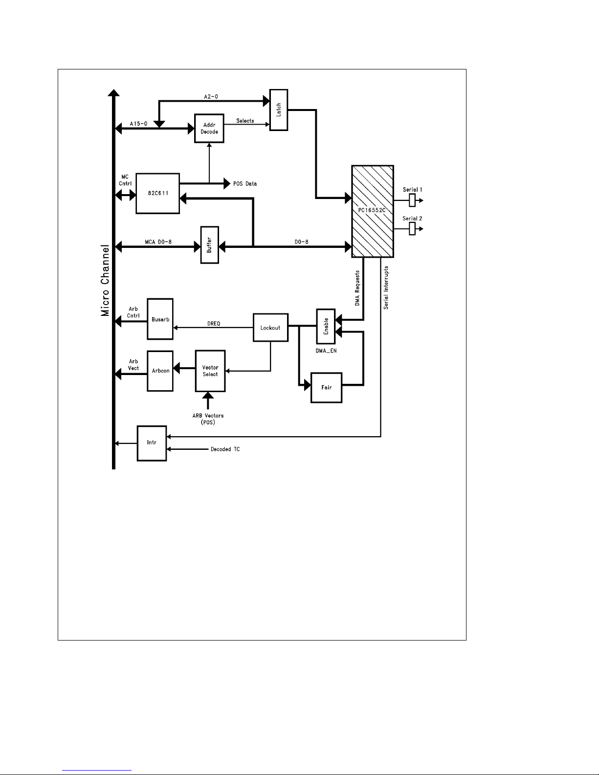
POSÐPROGRAMMABLE OPTION SELECT
A unique feature of Micro Channel machines is their Pro-
grammable Option Select, known as POS. POS eliminates
switches and jumpers from adapter cards by replacing their
function with programmable registers. The POS registers al-
low the system microprocessor to poll each adapter card to
determine its characteristics as well as write configuration
data to it. All resources required by an adapter (memory and
I/O addresses, interrupts used, DMA arbitration vectors,
etc.) can be relocatable and reconfigurable by the POS sys-
tem. Additionally, each card stores in POS registers a
unique ID number that the POS system uses to identify the
cards present in the system. A full understanding of the
POS mechanism is necessary before an adapter design is
undertaken. The IBM Technical Reference Manuals provide
details about POS that this document may not provide.
POS Mechanism
Each connector slot in the Micro Channel has a unique sig-
nal called CDSETUP that when asserted, puts the card resi-
dent in that slot in setup mode. The setup mode allows
access to a block of 8 POS registers located at I/O ad-
dresses 100h–107h. All cards in the system locate their
POS registers in this space but since only one card can be
placed in setup at a time, no conflicts can occur.
Micro Channel machines store in battery-backed CMOS
RAM the ID numbers of all resident adapters, the slot num-
bers they’re plugged into and the configuration data to be
written to their respective POS registers. During Power On
Self Test (POST), the system microprocessor puts each slot
in turn into setup mode and reads its ID. If it finds a valid ID
it sends the card its configuration data. If there is no card in
a slot, the microprocessor will read an ffH which it recogniz-
es as an empty slot.
Since the system remembers which adapter and ID resides
in each slot, removing a card, inserting a new card, or even
moving an existing card to a different slot will cause a POST
failure. IBM’s System Configuration utilities must then be run
to reconfigure the system by modifying the configuration
data stored in CMOS RAM.
ADFsÐAdapter Description Files
System board and adapter POS data is also stored on the
Reference diskette in the form of Adapter Description Files.
ADFs are given names corresponding to the ID of the card it
is to configure. The PC16552C Adapter has an ID number of
6E6Dh, giving it an ADF name of @6E6D.adf. A listing of
@6E6D.adf is included with this documentation.
The ADF is divided into sections which each list one or
more choices of resources to be allocated to the adapter
card. A given choice specifies the data to be loaded into a
particular POS register and also lists the resources allocat-
ed. For example, in @6E6D.adf, choosing ‘‘Serial 2’’
(COM2) for connector 1 will reserve the I/O address space
2f8–2ffh and will notify the system that IRQ3 is used. It also
specifies the data to be written to some of the bits in POS
registers 102 and 103. Note that pos[0]denotes POS102
and pos[1]denotes POS103 because registers POS100
and 101 contain the read-only card ID bytes which are not
referred to in ADFs. See PC16552C Adapter POS Register
Description for a description of the contents of the registers
used in this adapter.
The syntax for the ADF is straight forward and described in
detail in IBM’s Technical Reference manual. However, the
Configuration utilities are unforgiving of errors. Any errors in
a designer’s ADF will prevent any POS data for that card
from being loaded and the card from being enabled for op-
eration. In addition, the system will not boot to the operating
system while the new card is inserted until the ADF is cor-
rect and the system has been reconfigured with the new
data. One undocumented idiosyncrasy involves the 4-bit
fields for arbitration vectors. Since the system DMA control-
ler only recognizes vectors 0–7, only 3 bits are needed to
specify the vectors to be used on the card. However, the
Configuration utilities required that all four bits be specified,
including the most significant bit which is always 0.
Configuration Utilities
There are two different utilities on the Reference diskette
provided with the system which actually convert the ADFs to
configuration data in CMOS RAM. One of these utilities
must be run whenever a new card is installed. The first is
the Automatic Configuration program. It takes the first
choice in each resource list that will not cause a conflict with
other adapters in the system and automatically stores the
corresponding POS register data in CMOS RAM.
The second program is Set Configuration which allows the
user to manually select the resources desired. It first reads
the configuration data already in CMOS RAM and displays
the resources allocated to each installed card. It then allows
the user to change these choices of resources by displaying
one-by-one all of the options for that adapter listed in the
ADFs. After all new choices have been made, exiting the
program causes the new POS data to be loaded into CMOS
RAM and the system is reconfigured and re-booted.
3