Nexperia NX-HB-GAN039-TSCUL User manual

UM90008
NX-HB-GAN039-TSCUL 3.5 kW half-bridge evaluation board
with top-side cooled GaN FETs
Rev. 1.2 — 17 October 2023 user manual
Document information
Information Content
Keywords GaN FET, half-bridge, converter, evaluation board
Abstract The NX-HB-GAN039-TSCUL evaluation board is a half-bridge converter circuit using Nexperia
top-side cooled power GaN FETs.
Nexperia UM90008
NX-HB-GAN039-TSCUL 3.5 kW half-bridge evaluation board with top-side cooled GaN FETs
1. EVALUATION BOARD TERMS OF USE
The use of the Evaluation Board is subject to the Evaluation Board Terms of Use, which you can
find here. By using this Evaluation Board, you accept these terms.
2. High Voltage Safety Precautions
Read all safety precautions before use!
Please note that this document covers only the NX-HB-GAN039-TSCUL 3.5 kW half-bridge
evaluation board and its functions. For additional information, please refer to the Product
Specification
To ensure safe operation, please carefully read all precautions before handling the evaluation
board. Depending on the configuration of the board and voltages used, potentially lethal voltages
may be generated. Therefore, please make sure to read and observe all safety precautions
described below.
Before Use:
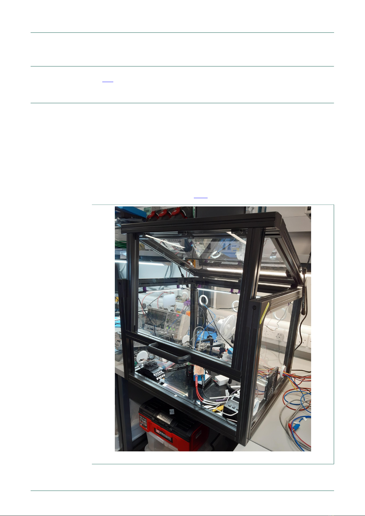
It is recommended that ALL operation and testing of the evaluation board is performed with the
board enclosed within a non-conductive enclosure that prevents the High Voltage supply to be
switched whilst open and accessible; see Fig. 1.
Fig. 1. Example of a safety enclosure in the Nexperia lab
UM90008 All information provided in this document is subject to legal disclaimers. © Nexperia B.V. 2023. All rights reserved
user manual Rev. 1.2 — 17 October 2023 2 / 24

Nexperia UM90008
NX-HB-GAN039-TSCUL 3.5 kW half-bridge evaluation board with top-side cooled GaN FETs
All probes should be position before turning on the High Voltage and should be held in place using
a suitable probe positioner e.g. PMK MSA100; see Fig. 2.
Fig. 2. Example of a probe positioner
Always use an oscilloscope with protective earth connected.
When probing High Voltage, ensure that the probes have the correct voltage rating / limit.
Ensure that all scope probes are compensated and de-skewed before use, refer to your
oscilloscope or probe manual for instructions on how to do this.
If possible, have a visual indicator of High Voltage located close to the evaluation board (LED bar
graph or voltmeter) To show when the Bus Voltage (Vbus) and Outputs are at dangerous levels.
Verify that none of the parts or components are damaged or missing.
Check that there are no conductive foreign objects on the board.
If any soldering or modifications are made or carried out, then please ensure that this is done
carefully so that solder splashes and debris are not created. Clean the board with Iso-propyl-
alcohol and allow it to dry.
Ensure that there is no condensation or moisture droplets on the circuit board, all testing should be
carried out within a dry environment without excessive humidity.
If used under conditions beyond the rated voltage and current specification, this may cause
defects, failure and or permanent damage.
NEVER handle the evaluation board during operation under ANY circumstances
After use the Nexperia Evaluation Board contains components which may store high voltage and
will take time to discharge. Carefully probe the evaluation board once the power has been removed
to check that all capacitors have been discharged. You must do this without touching the board
except for the multimeter probes that are being used to check.
This evaluation board is intended for use only in High Voltage Lab environments and should
be handled only by qualified personnel familiar with all safety and operating procedures. We
recommend carrying out operation and testing in a safe environment that includes restricted access
only to trained personnel, the use of High Voltage signage at all entrances, safety interlocks and
emergency stops and HV insulated flooring.
It should be noted that this evaluation board is intended to be used ONLY for evaluation purposes
and should not be used by consumers or designed into consumer equipment in its current form.
UM90008 All information provided in this document is subject to legal disclaimers. © Nexperia B.V. 2023. All rights reserved
user manual Rev. 1.2 — 17 October 2023 3 / 24
Nexperia UM90008
NX-HB-GAN039-TSCUL 3.5 kW half-bridge evaluation board with top-side cooled GaN FETs
3. Introduction
The NX-HB-GAN039-TSCUL top-side cooled half-bridge evaluation board provides the elements
of a simple buck or boost converter. This enables the basic study of the switching characteristics
and efficiency achievable with Nexperia’s 650 V GaN FETs. The circuit can be configured for
synchronous rectification, in either buck or boost mode. Selection jumpers allow the use of a single
logic input or separate high / low level inputs. The high-voltage input and output can operate at up
to 400 V DC, with a power output of up to 3.5 kW dependent upon cooling, ambient temperature
and switching frequency. The inductor provided is intended for efficient operation at 100 kHz,
however, other inductors and frequencies may be used.
The NX-HB-GAN039-TSCUL top-side cooled KIT is for evaluation purposes only. By using the
evaluation board you accept the terms of use, see GaN FET evaluation board Terms Of Use.
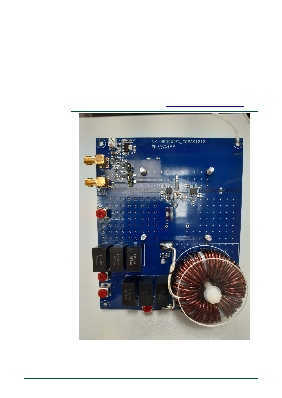
Fig. 3. NX-HB-GAN039-TSCUL top-side cooled half-bridge evaluation board
UM90008 All information provided in this document is subject to legal disclaimers. © Nexperia B.V. 2023. All rights reserved
user manual Rev. 1.2 — 17 October 2023 4 / 24
Nexperia UM90008
NX-HB-GAN039-TSCUL 3.5 kW half-bridge evaluation board with top-side cooled GaN FETs
3.1. Quick reference information
Table 1. NX-HB-GAN039-TSCUL top-side cooled Input/Output
Parameter Value
High-voltage input/output 400 VDC max
Auxiliary supply (J1) 10 V min, 18 V max
Logic inputs nominal 0 - 5 V
•for the pulse-generation circuit Vlo < 1.5 V, Vhi > 3.0 V
•for direct connection to gate drive Vlo < 0.8 V, Vhi > 2.0 V
SMA coaxial connectors
Switching frequency configuration dependent
•lower limit determined by peak inductor current
•upper limit determined by desired dead time and power dissipation
Power dissipation in the GaN FETs is limited by maximum junction temperature. Refer to the
GAN039-650NTB data sheet.
4. Warnings
This demo board is intended to demonstrate GaN FET technology. While it provides the main
features of a half-bridge converter, it is not intended to be a finished product and does not have all
the protection features found in commercial power supplies.
There is no specific protection against over-current or over-voltage on this board.
If the on-board pulse generation circuit is used in boost mode, a zero input corresponds to 100%
duty cycle for the active low-side switch.
UM90008 All information provided in this document is subject to legal disclaimers. © Nexperia B.V. 2023. All rights reserved
user manual Rev. 1.2 — 17 October 2023 5 / 24

Nexperia UM90008
NX-HB-GAN039-TSCUL 3.5 kW half-bridge evaluation board with top-side cooled GaN FETs
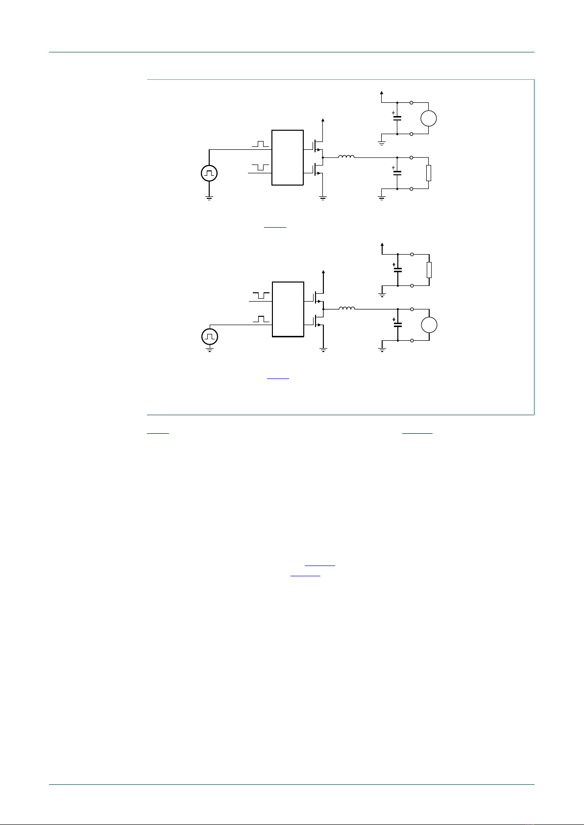
5. Circuit description
The circuit comprises a simple half-bridge featuring two GAN039-650NTB GaN FETs, as indicated
in the block diagram of Fig. 4. Two high-voltage ports are provided which can serve as either input
or output, depending on the configuration: boost or buck. In either case one GaN FET acts as
the active power switch while the other carries the freewheeling current. The latter device may
be enhanced, as a synchronous rectifier, or not. With GaN FETs the reverse recovery charge is
low and there is no need for additional freewheeling diodes. Two input connectors are provided
which can be connected to sources of logic-level command signals for the hi/lo gate driver. Both
inputs may be driven by off-board signal sources, or alternatively, a single signal source may be
connected to an on-board pulse-generator circuit which generates the two non-overlapping pulses.
Jumpers determine how the input signals are used.
An inductor is provided as a starting point for investigation. This is a 330 μH toroid intended to
demonstrate a reasonable compromise between size and efficiency for power up to 3.5 kW at a
switching frequency of 100 kHz.
aaa-028880
PULSE-GEN
CIRCUIT
HI/LO
GATE
DRIVER
HS GaN FET
LS GaN FET high voltage
buck output/
boost input
logic-level inputs
+HVDC
+HVDC
high voltage
buck input/
boost output
HS GaN FET and LS GaN FET = GAN039-650NTB
Fig. 4. Functional block diagram
6. Configuration
Fig. 5 shows the basic power connections for buck and boost modes. For buck mode, the HVDC
input (terminals J2, J3) is connected to the high-voltage supply and the output is taken from
terminals J5 and J7. For boost mode the connections are reversed.
Note that in boost mode a load must be connected. The load current affects the output voltage up
to the transition from DCM to CCM. In buck mode the load may be an open circuit. In the latter
case – buck mode, no load – the ripple current in the inductor is symmetric about zero, and the soft
switching behavior of the GaN FETs may be studied.
UM90008 All information provided in this document is subject to legal disclaimers. © Nexperia B.V. 2023. All rights reserved
user manual Rev. 1.2 — 17 October 2023 6 / 24
Nexperia UM90008
NX-HB-GAN039-TSCUL 3.5 kW half-bridge evaluation board with top-side cooled GaN FETs
aaa-028881
HI/LO
GATE
DRIVER
HS GaN FET
LS GaN FET
J2
J3
J5
J7
+HVDC
duty cycle = D
Vin\Vin
+HVDC
high voltage
input
+
-
Vout = D·HVDCload
(a) Buck Mode; see Fig. 4 regarding the complementary input
aaa-028882
HI/LO
GATE
DRIVER
HS GaN FET
LS GaN FET
J2
J3
J5
J7
+HVDC
duty cycle = D
Vin\
Vin
+HVDC
high voltage
input
Vs
+
-
Vout = Vs/(1-D)load
(b) Boost Mode; see Fig. 4 regarding the complementary input
HS GaN FET and LS GaN FET = GAN039-650NTB
Fig. 5. Supply and load connections for Buck (a) and Boost (b) configurations
Fig. 6 shows possible configurations for the gate-drive signals. In Fig 6(a) a single input from an
external signal source is used together with the on-board pulse generation circuit. J4 is used, J6 is
left open circuit. Jumpers JP1 and JP2 are in the top position, as shown. If the high-side transistor
is to be the active switch (e.g. buck mode), then the duty cycle of the input source should simply
be set to the desired duty cycle (D). If the low-side transistor is to be the active switch (e.g. boost
mode) the duty cycle of the input source should be set to (1-D), where D is the desired duty cycle
of the low-side switch.
Caution: If the on-board pulse-generation circuit is used for boost mode, be aware that a steady
state zero input (or disconnected signal source) will result in the low-side FET being turned
on continuously. Ensure that high voltage is not applied to J5 until the input is switching. This
configuration results in synchronous rectification. If it is desired to let the device carrying the
freewheeling current act as a diode, then the appropriate jumper should be placed so that the pull-
down resistor is connected to the driver. Fig 6(b) shows a buck-mode configuration where the low-
side device is not enhanced. Finally, Fig 6(c) shows use of two external signal sources as inputs to
the gate driver.
For any configuration an auxiliary supply voltage of 10 V - 18 V must be supplied at connector J1.
Pull-down resistors R5 and R6 have a value of 4.99 kΩ. If a 50 Ω signal source is used and
50 Ω termination is desired, then R5 and R6 may be replaced (or paralleled) with 1206 size 50 Ω
resistors.
UM90008 All information provided in this document is subject to legal disclaimers. © Nexperia B.V. 2023. All rights reserved
user manual Rev. 1.2 — 17 October 2023 7 / 24

Nexperia UM90008
NX-HB-GAN039-TSCUL 3.5 kW half-bridge evaluation board with top-side cooled GaN FETs
aaa-028883
PULSE-GEN
CIRCUIT
HI/LO
GATE
DRIVER
JP1
1
HS GaN FET
LS GaN FET
+HVDC
Vin
JP2
1
J4
J6
(a)
aaa-028884
PULSE-GEN
CIRCUIT
HI/LO
GATE
DRIVER
0
HS GaN FET
LS GaN FET
+HVDC
Vin
JP2
1
JP1
1
J4
J6
(b)
aaa-028885
PULSE-GEN
CIRCUIT
HI/LO
GATE
DRIVER
HS GaN FET
LS GaN FET
+HVDC
Vin
Vin\ JP2
1
J4
J6
JP1
1
(c)
HS GaN FET and LS GaN FET = GAN039-650NTB
Fig. 6. Input configurations. (a) using a single source for either buck or boost mode
(b) buck mode without synchronous rectification (c) using two signal sources
7. Design details
For this evaluation board, the half-bridge converter circuit has been implemented on a 4-layer PCB
and uses two Nexperia GAN039-650NTB GaN FETs.
The circuit schematic, PCB layout and bill of materials for the NX-HB-GAN039-TSCUL top-side
cooled evaluation board are shown in the next sections.
UM90008 All information provided in this document is subject to legal disclaimers. © Nexperia B.V. 2023. All rights reserved
user manual Rev. 1.2 — 17 October 2023 8 / 24

Nexperia UM90008
NX-HB-GAN039-TSCUL 3.5 kW half-bridge evaluation board with top-side cooled GaN FETs
7.1. NX-HB-GAN039-TSCUL top-side cooled schematic
Fig. 7. Schematic
UM90008 All information provided in this document is subject to legal disclaimers. © Nexperia B.V. 2023. All rights reserved
user manual Rev. 1.2 — 17 October 2023 9 / 24

Nexperia UM90008
NX-HB-GAN039-TSCUL 3.5 kW half-bridge evaluation board with top-side cooled GaN FETs
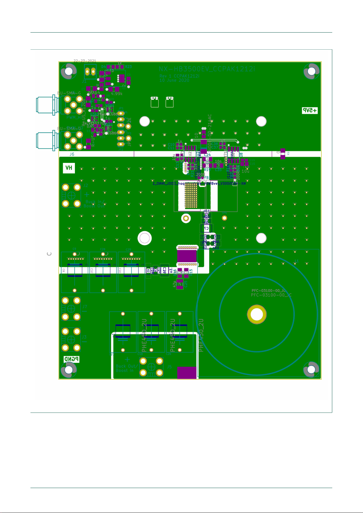
7.2. NX-HB-GAN039-TSCUL top-side cooled PCB layout
Fig. 8. PCB top layer, HV
UM90008 All information provided in this document is subject to legal disclaimers. © Nexperia B.V. 2023. All rights reserved
user manual Rev. 1.2 — 17 October 2023 10 / 24
Nexperia UM90008
NX-HB-GAN039-TSCUL 3.5 kW half-bridge evaluation board with top-side cooled GaN FETs
Fig. 9. PCB bottom layer, power ground
UM90008 All information provided in this document is subject to legal disclaimers. © Nexperia B.V. 2023. All rights reserved
user manual Rev. 1.2 — 17 October 2023 11 / 24

Nexperia UM90008
NX-HB-GAN039-TSCUL 3.5 kW half-bridge evaluation board with top-side cooled GaN FETs
Fig. 10. PCB inner layer 2, power ground
UM90008 All information provided in this document is subject to legal disclaimers. © Nexperia B.V. 2023. All rights reserved
user manual Rev. 1.2 — 17 October 2023 12 / 24

Nexperia UM90008
NX-HB-GAN039-TSCUL 3.5 kW half-bridge evaluation board with top-side cooled GaN FETs
Fig. 11. PCB inner layer 15, HV
UM90008 All information provided in this document is subject to legal disclaimers. © Nexperia B.V. 2023. All rights reserved
user manual Rev. 1.2 — 17 October 2023 13 / 24

Nexperia UM90008
NX-HB-GAN039-TSCUL 3.5 kW half-bridge evaluation board with top-side cooled GaN FETs
Fig. 12. PCB silkscreen
UM90008 All information provided in this document is subject to legal disclaimers. © Nexperia B.V. 2023. All rights reserved
user manual Rev. 1.2 — 17 October 2023 14 / 24
Nexperia UM90008
NX-HB-GAN039-TSCUL 3.5 kW half-bridge evaluation board with top-side cooled GaN FETs
7.3. NX-HB-GAN039-TSCUL top-side cooled Bill of Materials (BOM)
Table 2. NX-HB-GAN039-TSCUL Bill of Materials
Part Value Package Description Supplier Supplier p/n Voltage
C1 22u C1206 Capacitor, ceramic Farnell 2525173 35V
C2 1u C0805 Capacitor, ceramic Farnell 2094043 50V
C3 2.2u C0805 Capacitor, ceramic Farnell 2346931 50V
C4 10n C1206_3216Metric Capacitor, ceramic Farnell 1759518 630V
C5 10n C1206_3216Metric Capacitor, ceramic Farnell 1759518 630V
C6 10n C1206 Capacitor, ceramic Farnell 1759518 630V
C7 .1u C_1812_4532Metric Capacitor, ceramic Farnell 2085218 1KV
C8 .1u C2225K Capacitor, ceramic Farnell 1838767 or
2896821
1KV
C9 2.2uF Panasonic ECWFE2W225K Farnell 2581173 450V
C10 .1u C0603 Capacitor, ceramic Farnell 2749806 100V
C11 .1u C0603 Capacitor, ceramic Farnell 2749806 100V
C12 .1u C0603 Capacitor, ceramic Farnell 2749806 100V
C13 10u C0805 Capacitor, ceramic Farnell 2528772 35V
C14 .1u C0603 Capacitor, ceramic Farnell 2749806 100V
C15 10u C0805 Capacitor, ceramic Farnell 2528772 35V
C16 .1u C2225K Capacitor, ceramic Farnell 1838767 or
2896821
1KV
C17 .1u C2225K Capacitor, ceramic Farnell 1838767 or
2896821
1KV
C18 2.2uF Panasonic ECWFE2W225K Farnell 2581173 450V
C19 100pF C0603 Capacitor, ceramic Farnell 1740605 100V
C20 .1u C0603 Capacitor, ceramic Farnell 2749806 100V
C21 .1u C0603 Capacitor, ceramic Farnell 2749806 100V
C22 .1u C0603 Capacitor, ceramic Farnell 2749806 100V
C23 220pF C0603 Capacitor, ceramic Farnell 498579 100V
C24 10n C1206_3216Metric Capacitor, ceramic Farnell 1759518 630V
C25 47p C1210 Capacitor, ceramic Farnell 1855914 1KV
C26 2.2uF Panasonic ECWFE2W225K Farnell 2581173 450V
C27 2.2uF Panasonic ECWFE2W225K Farnell 2581173 450V
C28 2.2uF Panasonic ECWFE2W225K Farnell 2581173 450V
C29 2.2uF Panasonic ECWFE2W225K Farnell 2581173 450V
C30 .1u C2225K Capacitor, ceramic Farnell 1838767 or
2896821
1KV
C31 .1u C2225K Capacitor, ceramic Farnell 1838767 or
2896821
1KV
C32 .1u C2225K Capacitor, ceramic Farnell 1838767 or
2896821
1KV
C33 10n C1206_3216Metric Capacitor, ceramic Farnell 1759518 630V
C34 10n C1206_3216Metric Capacitor, ceramic Farnell 1759518 630V
C35 10n C1206_3216Metric Capacitor, ceramic Farnell 1759518 630V
C36 .1u C_1812_4532Metric Capacitor, ceramic Farnell 2085218 1KV
C37 .1u C0603 Capacitor, ceramic Farnell 2749806 100V
UM90008 All information provided in this document is subject to legal disclaimers. © Nexperia B.V. 2023. All rights reserved
user manual Rev. 1.2 — 17 October 2023 15 / 24

Nexperia UM90008
NX-HB-GAN039-TSCUL 3.5 kW half-bridge evaluation board with top-side cooled GaN FETs
Part Value Package Description Supplier Supplier p/n Voltage
C38 .1u C0603 Capacitor, ceramic Farnell 2749806 100V
D1 ES1J DO-214AC DIODE Farnell 2677373 600V
D2 BAT54 SOT23 Schottky Diodes Farnell 1081190
D3 BAT54 SOT23 Schottky Diodes Farnell 1081190
D4 LED LED_0805_2012 Metric 2.0 x 1.25mm SMD
CHIP LED
Farnell 2610419
FB1 30R R_0603_1608 Metric ferrite bead Farnell 1515741
FB2 30R R_0603_1608 Metric ferrite bead Farnell 1515741
HS1 Heatsink COOL_INNO_1 SR_Heatsinks Cool Innovations 3-282810MS76855
Heatsink Insulator Shim AIN 40 mm x 40 mm x 0.5 mm SFXPCB 345-1548-ND
Heatsink thermal paste Farnell 725572
J1 22-23-2021 2.54mm 2 pin header Farnell 1462926
J2 terminal block KEYSTONE_ 8191-2 Screw terminal Mouser 534-8191-2
J3 terminal block KEYSTONE_ 8191-2 Screw terminal Mouser 534-8191-2
J4 BU-SMA-G BU-SMA-G FEMALE SMA
CONNECTOR
Farnell 2112448
J5 terminal block KEYSTONE_ 8191-2 Screw terminal Mouser 534-8191-2
J6 BU-SMA-G BU-SMA-G FEMALE SMA
CONNECTOR
Farnell 2112448
J7 terminal block KEYSTONE_ 8191-2 Screw terminal Mouser 534-8191-2
JP1 Pin Header 2.54mm 3-pin header Farnell 1248150
JP2 Pin Header 2.54mm 3-pin header Farnell 1248150
L1 330uH HB Inductor PFC-03100-00_JC ACAL BFI/
Cambridge
55439A2 MPP
CORE
R1 4.99k R1206 Resistor Farnell 1470015
R2 499k R1206 Resistor Farnell 1470019
R3 10MEG R1206 Resistor Farnell 1469973
R4 10R R0805 Resistor Farnell 2303326
R5 51R R1206 Resistor Farnell 1470021
R6 51R R1206 Resistor Farnell 1470021
R7 15R R0603 Resistor RS Components 122-3692
R8 1k R0603 Resistor Farnell 1469740
R9 0R R1206 Resistor Farnell 1469963
R10 1k5 R0603 Resistor Farnell 1469743
R11 15R R0603 Resistor RS Components 122-3692
R15 15 R1206 Resistor Farnell 9236660
R16 15 R1206 Resistor Farnell 9236660
R17 10 R1206 Resistor Farnell 1738986
R18 10 R1206 Resistor Farnell 1738986
R19 10 R1206 Resistor Farnell 1738986
R21 15R R0603 Resistor RS Components 122-3692
R22 15R R0603 Resistor RS Components 122-3692
TP1 TPSPAD1-13 P1-13 TEST PIN Farnell 1463077
TP2 TPSPAD1-13 P1-13 TEST PIN Farnell 1463077
TP3 TPSPAD1-13 P1-13 TEST PIN Farnell 1463077
UM90008 All information provided in this document is subject to legal disclaimers. © Nexperia B.V. 2023. All rights reserved
user manual Rev. 1.2 — 17 October 2023 16 / 24

Nexperia UM90008
NX-HB-GAN039-TSCUL 3.5 kW half-bridge evaluation board with top-side cooled GaN FETs
Part Value Package Description Supplier Supplier p/n Voltage
TP4 TPSPAD1-13 P1-13 TEST PIN Farnell 1463077
TP5 TPSPAD1-13 P1-13 TEST PIN Farnell 1463077
U1 LT3082 SOT223-3 Linear Regulator Mouser 584-LT3082EST
#PBF
U2 Si8271BB-IS SOIC-8_ 3.9x4.9mm_
P1.27mm
Hi/Lo Iso gate driver Farnell 2524443
U3_A1 74LVC1G17GW SOT353-1 Schmitt Trigger buffer Nexperia 74LVC1G17GW
U4_B1 74AUP1G86GW SOT353-1 2-input X-OR gate Nexperia 74AUP1G86GW
U5_B1 74AUP1G86GW SOT353-1 2-input X-OR gate Nexperia 74AUP1G86GW
U6 GAN039-650NTB CCPAK1212i GaN FET Nexperia GAN039-650NTB
U7 GAN039-650NTB CCPAK1212i GaN FET Nexperia GAN039-650NTB
U8 Si8271BB-IS SOIC-8_ 3.9x4.9mm_
P1.27mm
Hi/Lo Iso gate driver Farnell 2524443
Washers for Heatsink (x4) M4 Nylon washer Farnell 2472665
Nut For Heatsink M4 Nylon nut Farnell 7016955
Standoffs (x4) M3 x 60mm stand off RS Components 664-3347
Washers for Standoff (x8) M3 Nylon washer Farnell 2472664
Nut for Standoff M3 Nylon nut Farnell 2472687
Spacer for Top Side
Cooled Heatsink
M4 x 3mm Nylon Spacer Farnell 2837901
Standoffs (x4) M3 x 60mm stand off RS Components 664-3347
Inductor Holder Plastic Disc 46mm x 3mm
Inductor Nut Nylon Nut M5 Farnell 7016967
Inductor Screw Nylon Screw M5 x 40mm Farnell 2472726
Inductor Washer Nylon Washer M5 Farnell 2472666
8. Using the board
The board can be used for evaluation of basic switching functionality in a variety of circuit
configurations. It is not a complete circuit, but rather a building block. It can be used in steady-state
DC/DC converter mode with output power up to 3.5 kW.
UM90008 All information provided in this document is subject to legal disclaimers. © Nexperia B.V. 2023. All rights reserved
user manual Rev. 1.2 — 17 October 2023 17 / 24
Nexperia UM90008
NX-HB-GAN039-TSCUL 3.5 kW half-bridge evaluation board with top-side cooled GaN FETs
9. Dead time control
The required form of the gate-drive signals is shown in Fig. 13. The times marked A are the
deadtimes when neither transistor is driven on. The deadtime must be greater than zero to avoid
shoot-through currents. The Si8271 Gate driver does not provide deadtime setting for the half
bridge. The deadtime between high side and low side drivers is provided by U5B1 and U4B1 using
their RC timing components. The typical setting provides 100 nS dead time.
VGS 1
VGS 2
Fig. 13. Non-overlapping gate pulses
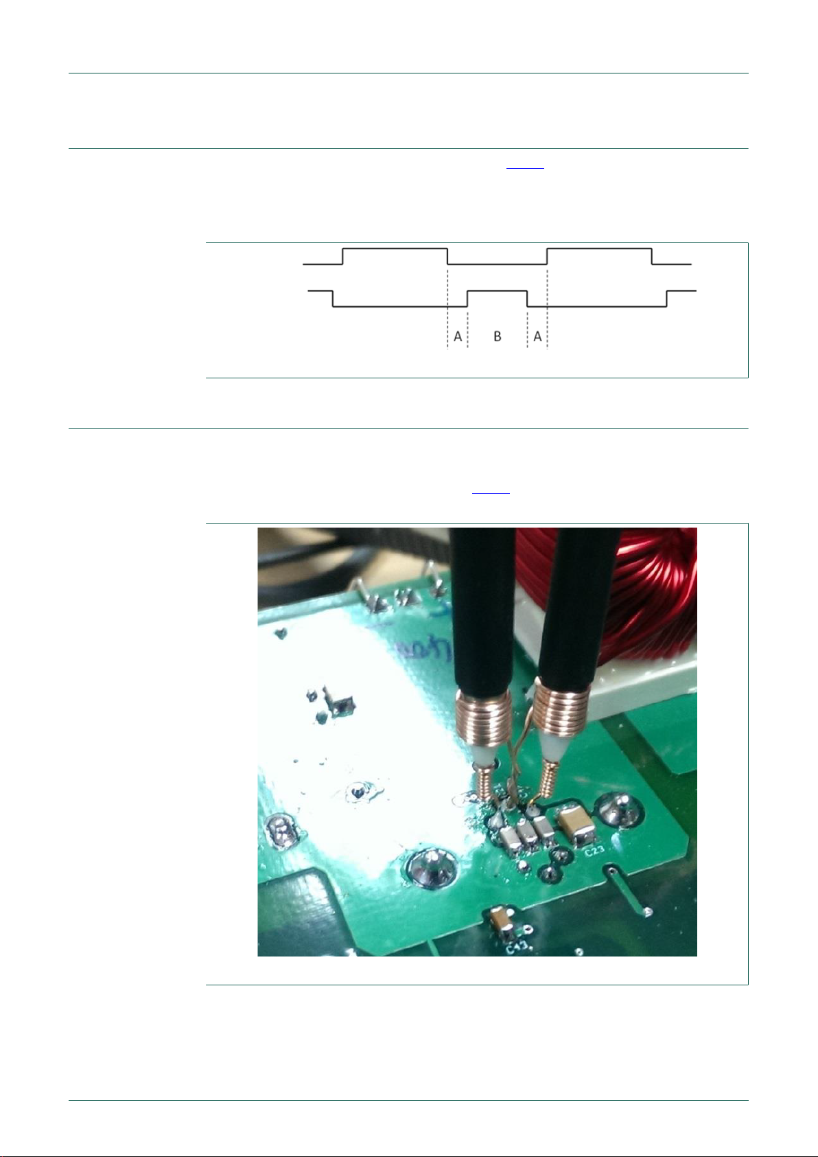
10. Probing
Test points 2 and 5 (TP2, TP5) are provided for probing the switching waveform. In order to
minimize inductance during measurement, the tip and the ground of the probe should be directly
attached to the sensing points to minimize the sensing loop. Coiled bus wire can be effectively
used to make these connections, as indicated in Fig. 14. See Nexperia application note AN90004
for further details.
Fig. 14. Low-inductance probing of fast, high-voltage signals
UM90008 All information provided in this document is subject to legal disclaimers. © Nexperia B.V. 2023. All rights reserved
user manual Rev. 1.2 — 17 October 2023 18 / 24
Nexperia UM90008
NX-HB-GAN039-TSCUL 3.5 kW half-bridge evaluation board with top-side cooled GaN FETs
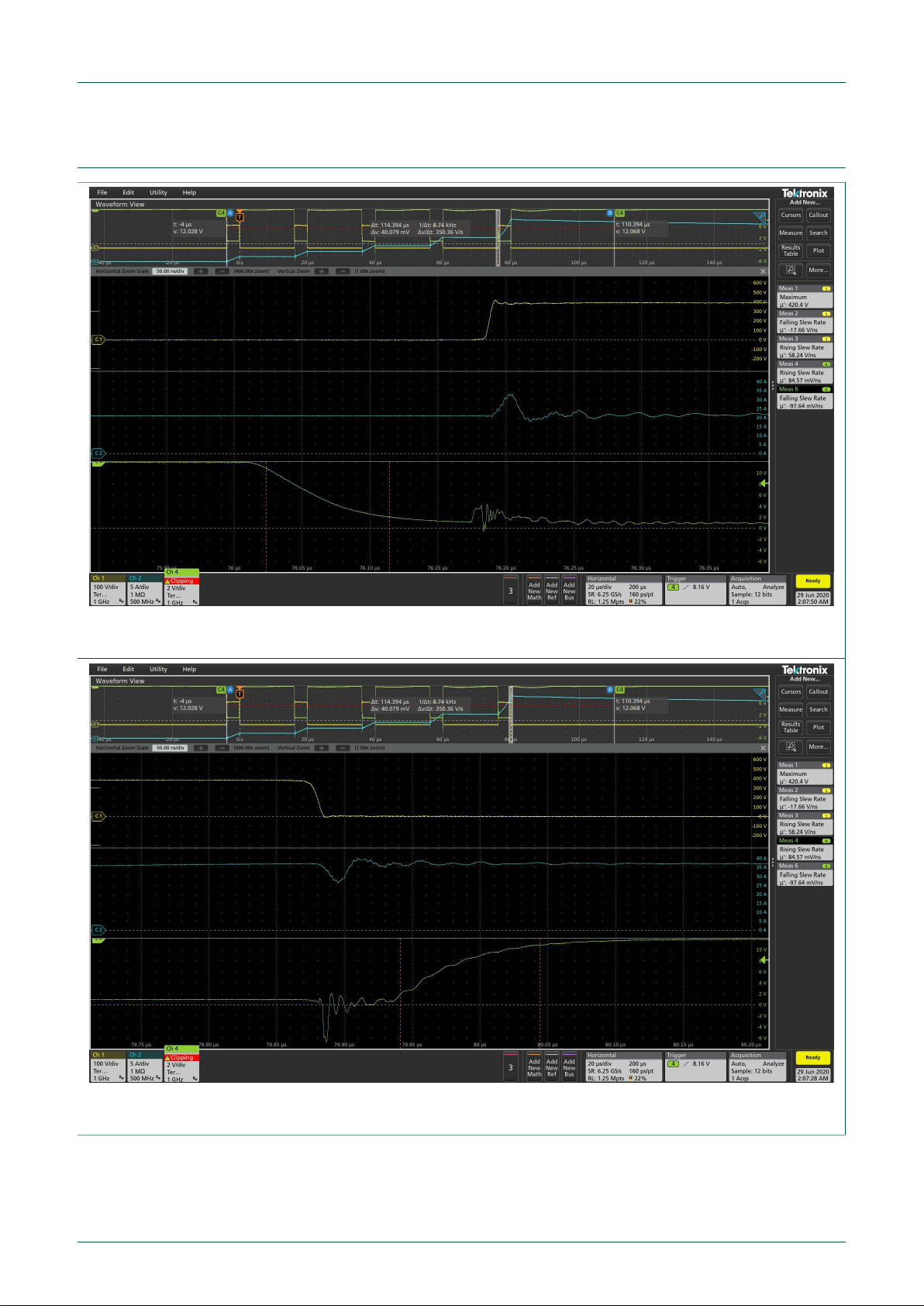
11. Typical switching waveforms
Channel 1 - Yellow = Switching node; Channel 2 - Blue = Inductor current; Channel 4 - Green = LS VGS
Fig. 15. Turn off @ 20 Amps
Channel 1 - Yellow = Switching node; Channel 2 - Blue = Inductor current; Channel 4 - Green = LS VGS
Fig. 16. Turn on @ 35 Amps
UM90008 All information provided in this document is subject to legal disclaimers. © Nexperia B.V. 2023. All rights reserved
user manual Rev. 1.2 — 17 October 2023 19 / 24

Nexperia UM90008
NX-HB-GAN039-TSCUL 3.5 kW half-bridge evaluation board with top-side cooled GaN FETs
12. Efficiency sweep
Efficiency has been measured for this circuit in buck mode with a 400 VDC input and 230 VDC
output, switching at 100 kHz.
aaa-032324
96
94
98
100
Efficiency
(%)
92
Output power (W)
0 400030001000 2000
Fig. 17. Efficiency for a buck converter 400 V : 230 V
13. Revision history
Table 3. Revision history
Revision
number
Date Description
1.2 20231017 High Voltage Safety Precautions added. Evaluation board name changed from
NX-HB3500EV-CCPAK1212i to NX-HB-GAN039-TSCUL.
1.1 20211014 Initial version Fig. 12 added.
1.0 20200911 Preliminary version.
UM90008 All information provided in this document is subject to legal disclaimers. © Nexperia B.V. 2023. All rights reserved
user manual Rev. 1.2 — 17 October 2023 20 / 24
Table of contents
Other Nexperia Motherboard manuals


