Nexperia NBM5100 User manual

Nexperia UM90022
NBM5100; NBM7100 Evaluation board module
1. Introduction
The NBM5100x and NBM7100x are battery booster integrated circuits intended to expand the
lifetime and current capability of a coin cell battery like CR2032 and Lithium Thionyl batteries.
This manual gives a quick start of the NBM5100x and NBM7100x evaluation boards usage
together with the PC application or standalone.
The NBM5100x, NBM7100x evaluation board is fully assembled, containing all necessary
components to evaluate the performance and behavior of these battery boosters.
In total 4 variants of the evaluation board are available:
Table 1. Evaluation board variants
Evaluation
board variant
Bus interface Auto start
mode
Storage
Cap Charge
Balance
Function
Max Storage
Cap Voltage
Max Load
Current
NBM7100A I²C + - 11 V 200 mA
NBM5100A I²C + + 5.5 V 150 mA
NBM7100B SPI - - 11 V 200 mA
NBM5100B SPI - + 5.5 V 150 mA
All variants use the same PCB design and expose a USB to SPI/USB to I²C interface to allow
control of the Battery booster from a PC application.
2. Hardware description
The Evaluation Board enables evaluation of the Battery Booster products by controlling them from
a PC or connection to a board under development. The NBM5100x, NBM7100x evaluation kit is
fully assembled, containing apart from a CR2032 battery cell all necessary components to evaluate
the performance and behavior of the battery boosters before applying them in an application. The
top area of the PCB contains an USB to I²C and USB to SPI converter and a level shifter circuit for
controlling the Evaluation board with a PC GUI application. The following sections give a detailed
overview of the module and available test pins for observing the behavior.
2.1. Storage capacitor
By default, one storage capacitor is mounted for the NBM7100x series. For the NBM5100x two
(balanced) super capacitors are mounted in series. The size of these capacitors depends on the
amount of energy needed to supply the load. For demonstration purposes 1000 µF capacitors
are placed on the NBM7100x board and 470 mF for the NBM5100x board. Both boards offer the
possibility to mount leaded (super-) capacitors. It is also possible to connect a custom storage
capacitor to connector J6.
UM90022 All information provided in this document is subject to legal disclaimers. © Nexperia B.V. 2023. All rights reserved
user manual Rev. 1 — 11 July 2023 2 / 21

Nexperia UM90022
NBM5100; NBM7100 Evaluation board module
2.2. Breakout board
Fig. 1. Breakout DIL converter board
The Evaluation board also includes a DIL converter board, which can be broken from the Main
PCB. Removing it from the main board will not impact the operation of it, as the board is electrically
not connected to it. This enables an easy evaluation of the product in an application prototype or
on a breadboard. An inductor was not included on the board and has to be connected externally to
allow evaluation of different inductors. The Pin numbers on the TOP side silkscreen directly map to
the pin numbers of the battery booster IC.
2.3. Jumper description
Fig. 2. Top view
Fig. 3. Bottom view
UM90022 All information provided in this document is subject to legal disclaimers. © Nexperia B.V. 2023. All rights reserved
user manual Rev. 1 — 11 July 2023 3 / 21

Nexperia UM90022
NBM5100; NBM7100 Evaluation board module
Table 2. Evaluation board variants
Jumper
name
PCB
side
Position Description
1-2 (Left) Selects 7-bit I²C address 0x2e
2-3 (Right) Selects 7-bit I²C address 0x2f
JP1 Top
Open Mandatory position for NBM5100B and NBM7100B (SPI variants)
1-2 (top) Selects PC (FTDI) to drive the Load matrix.JP2 Top
2-3 (bot) Selects NBM RDY signal to drive the Load matrix.
Closed Connects the Battery positive pole and the external power supply
input to the supply input to Battery supply of NBM.
JP3 Top
Open External J2 supply input is not connected.
JP4 Bottom Closed Mandatory position to ground TST pin. Don’t open this jumper.
JP5 Top Open Disconnect Balance pin from capacitors.
Closed Connect Balance pin to center pin of series capacitors. Mandatory
for NBM5100A & NBM5100B board in their default configuration.
JP6 Top Open Don’t bypass low side capacitor. This is required for NBM5100A /
NBM5100B boards which have 2 capacitors in series.
Closed Mandatory position for NBM7100A and NBM7100B variants to
connect the negative pin of the storage capacitor to ground.
Open Disconnect on board capacitor.JP7 Top
Closed Connect on board storage capacitor(s) to CAP pin of NBM.
The intention of this pin it to give the ability to measure the
charging current.
JP8 Top Close Default position. Connects the on board inductor to NBM. The
Jumper can be used to measure the coil current. Default should
be closed, when removed the IC will not operate correctly.
Open Disconnect VDHs (sense) line from VDH output.JP9 Bottom
Close Default position. Connects VDHs to VDH output.
JP10 Top Open Connects VDH output of NBM to connector J7 and can be used to
measure the load current.
Close Disconnects VDH output from JP7. Useful to disconnect all loads
from Battery booster.
P12 Top Option to connect an external load which can be controlled over
the Load Matrix and on-board FET. Remove R24 to use this
feature, in case the load is high ohmic.
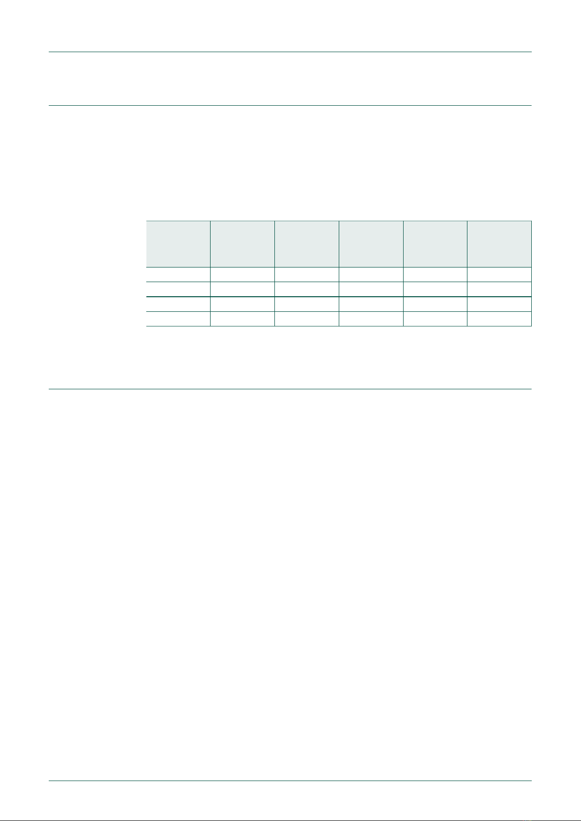
Pin header JP2 and J9 (Load Matrix)
The Load Matrix is a circuit (see Fig. 4) to simulate load current pulses for evaluation purposes.
Multiple loads in form of resistors are present in the load matrix. An additional LED is present to
show a visual representation of a capacitor loading. The loads are switched with Transistors. Using
a Jumper bank the source of the load signal, but also the load current can be set.
UM90022 All information provided in this document is subject to legal disclaimers. © Nexperia B.V. 2023. All rights reserved
user manual Rev. 1 — 11 July 2023 4 / 21

Nexperia UM90022
NBM5100; NBM7100 Evaluation board module
Fig. 4. Load matrix circuit
As visible from above picture the center pin row of the 6x3 pin header connects to the FET gate
pins for load actuation. The left side connects to SMB connector J8 for external load triggering.
The right side connects depending on Jumper JP2 setting either to the FTDI for actuation of a load
pulse from the PC GUI application (future GUI extension, JP2 position 1-2) or to the NBM RDY pin
(JP2 position 2-3).
Fig. 5. Load matrix Jumper pins
Multiple jumpers can be placed at the same time to add up the individual currents.
UM90022 All information provided in this document is subject to legal disclaimers. © Nexperia B.V. 2023. All rights reserved
user manual Rev. 1 — 11 July 2023 5 / 21
Nexperia UM90022
NBM5100; NBM7100 Evaluation board module
Table 3. Evaluation board variants
Row
(enumerated from top to bottom)
Approximate current
(VDP = 3.6 V)
Comment
1 1 mA -
2 10 mA -
3 20 mA -
4 50 mA -
5 100 mA -
6 200 mA This selection supplies a high
power LED
Example jumper placement to select 200 mA LED as current sink driven by the NBM ready signal
is shown in Fig. 6.
Fig. 6. Jumper placement to select 200 mA LED
Delivery state jumper settings
When the boards get delivered, they use different jumper settings. Below table summarizes the
default jumper setting.
Table 4. Delivery state jumper settings
Jumper NBM5100A
Default position
NBM5100B
Default position
NBM7100A
Default position
NBM7100B
Default position
JP1 0x2E open 0x2E open
JP2 2-3 2-3 2-3 2-3
JP3 closed closed closed closed
JP4 closed closed closed closed
JP5 closed closed open open
JP6 open open closed closed
JP7 closed closed closed closed
JP8 closed closed closed closed
JP9 closed closed closed closed
JP10 closed closed closed closed
JP12 open open open open
UM90022 All information provided in this document is subject to legal disclaimers. © Nexperia B.V. 2023. All rights reserved
user manual Rev. 1 — 11 July 2023 6 / 21

Nexperia UM90022
NBM5100; NBM7100 Evaluation board module
2.4. Connector description
Fig. 7. Connector description
Pin header J1 (Digital TP)
This jumper block makes all digital IO signals available. Depending on the Battery booster type, the
pins have different usages.
Pin header J4 (SPI)
Table 5. Pin header J4 (SPI)
NBM5100A
NBM7100A
NBM5100B
NBM7100B
NBM5100A
NBM7100A
NBM5100B
NBM7100B
SDI = START pin
for auto mode
SDI = SPI MOSI
pin
GND GND
CSN = I²C
address select
CSN = SPI chip
select pin
GND GND
RDY = ready signal (output) GND GND
SDA = I²C data SDA = SPI MISO GND GND
SCL = I²C clock SCL = SPI SCLK GND GND
UM90022 All information provided in this document is subject to legal disclaimers. © Nexperia B.V. 2023. All rights reserved
user manual Rev. 1 — 11 July 2023 7 / 21

Nexperia UM90022
NBM5100; NBM7100 Evaluation board module
Pin header J3 (I²C)
Table 6. Pin header J3 (I²C)
NBM5100A
NBM7100A
NBM5100B
NBM7100B
GND
SDA = I²C data SDA = SPI MISO
VDP = VDP voltage output from NBM
(the intention is to provide an IO voltage level reference)
SCL = I²C clock SCL = SPI SCLK
Pin Header J7 (Output)
Table 7. Pin Header J7 (Output)
NBM5100A
NBM7100A
NBM5100B
NBM7100B
OUT = VDH output voltage from NBM. (ensure jumper JP10 is
placed)
GND
VDHs = VDH sense signal to NBM. Default-wise it is connected
to the OUT pin using solder-jumper JP9
Pin Header J6 (External capacitor)
Use this pin header to connect an external capacitor. An external capacitor can be used in parallel
to the mounted one. In case only an external capacitor should be used, it is required to desolder
the mounted capacitor.
Table 8. Pin Header J6 (External capacitor)
NBM5100A
NBM7100A
NBM5100B
NBM7100B
- = GND
+ = Positive capacitor terminal
SMB connector J8 (Load)
The Load connector can be used to connect an external function generator (or microcontroller) to
create a timed load pulse for product evaluation. The center pin of the connector connects to the
left side pins of the J9 load selector pin header. The input impedance is high-ohmic.
UM90022 All information provided in this document is subject to legal disclaimers. © Nexperia B.V. 2023. All rights reserved
user manual Rev. 1 — 11 July 2023 8 / 21

Nexperia UM90022
NBM5100; NBM7100 Evaluation board module
Table 9. SMB connector J8 (Load)
NBM5100A
NBM7100A
NBM5100B
NBM7100B
SMB male connector
SMB connector J5 (Start)
The Start connector can be used to connect an external function generator to generate a Start
pulse to the battery booster IC (evaluation of autonomous mode). The input impedance is 100 kΩ.
Table 10. SMB connector J5 (Start)
NBM5100A
NBM7100A
NBM5100B
NBM7100B
SMB male connector
UM90022 All information provided in this document is subject to legal disclaimers. © Nexperia B.V. 2023. All rights reserved
user manual Rev. 1 — 11 July 2023 9 / 21
Nexperia UM90022
NBM5100; NBM7100 Evaluation board module
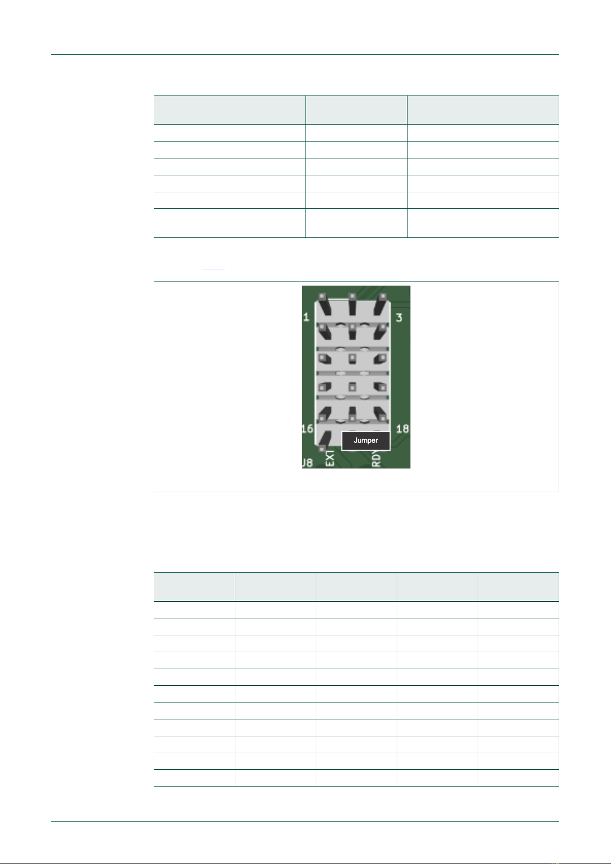
3. Test points
Many test points are provided to observe waveforms or voltage levels of the Battery booster. A
description of the test point location and connection is listed below.
Fig. 8. Test points
Table 11. Pin header J4 (SPI)
Test pin name Connected to Description
TP1 External Supply + pin Measure point for input supply voltage
TP2 GND
TP3 GND Ground bar. Use to connect an oscilloscope probe
ground lead.
TP4 VBT VBT voltage going to VBT pin of NBM.
TP5 TST Do not use.
TP6 BAL Balance pin measurement point. Useful for NBM5100 to
measure capacitor voltage of each capacitor.
TP7 CAP Capacitor positive terminal, connected to CAP pin of
NBM.
TP8 VDP Connected to VDP pin of NBM.
TP9 LX1 LX1 inductor pin.
TP10 LX2 LX2 inductor pin.
TP11 Pin 2: VDH
Pin 1: GND
Measurement point for VDH output in case Jumper J10
is open.
TP12 VDHs VDH Sense input. In case solder Jumper JP9 is opened,
it can be used to inject an externally supplied sense
signal.
TP13 GND Ground bar. Use to connect an oscilloscope probe
ground lead
UM90022 All information provided in this document is subject to legal disclaimers. © Nexperia B.V. 2023. All rights reserved
user manual Rev. 1 — 11 July 2023 10 / 21
Nexperia UM90022
NBM5100; NBM7100 Evaluation board module
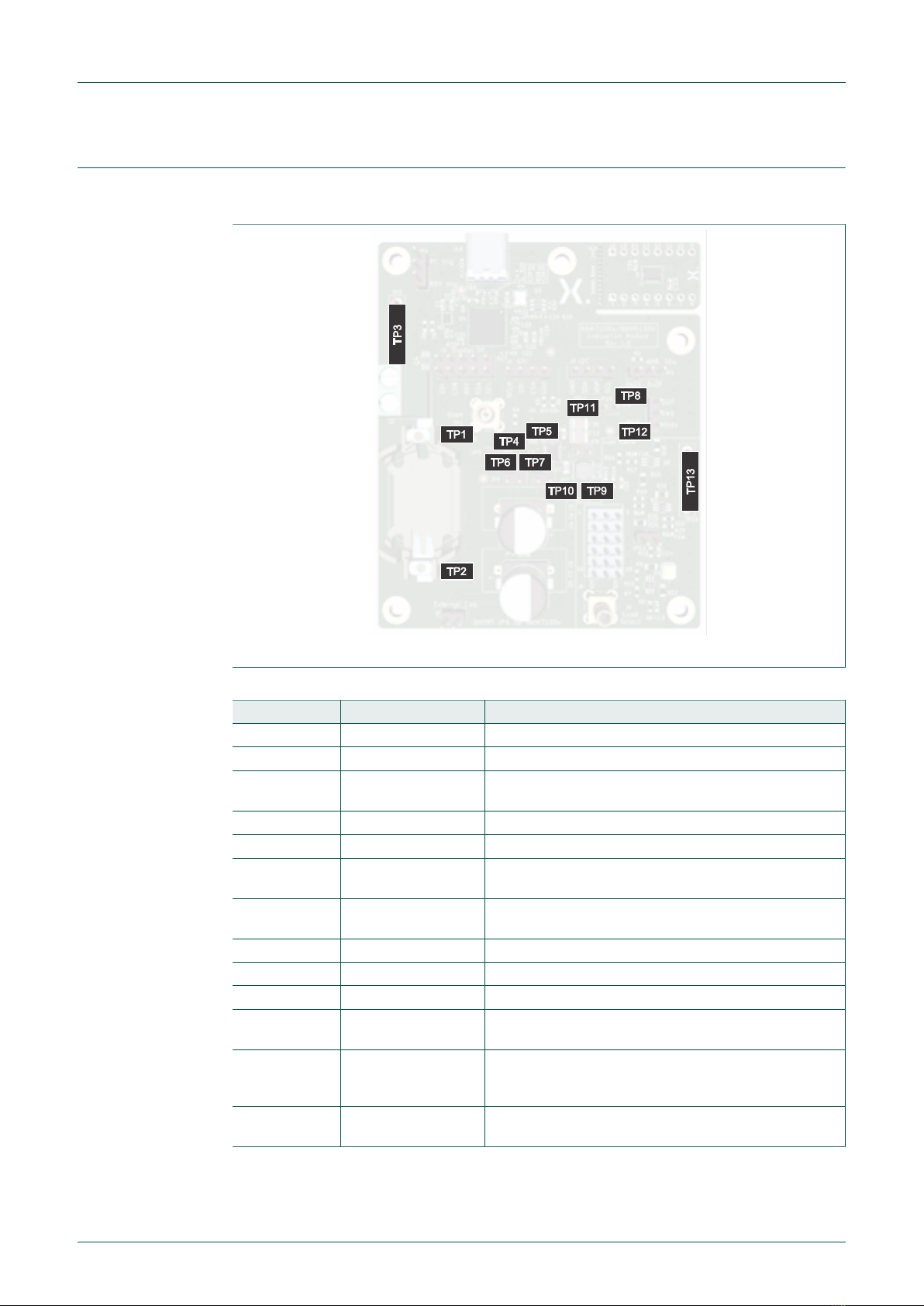
4. Using the Evaluation board with PC
Below steps are assuming as precondition, that the board is in default jumper setting state. Insert a
CR2032 Battery into the coin cell holder or supply externally 3 V to the supply connector J2. Next
connect the Evaluation board to the PC. When connecting it the first time a driver will be installed
automatically by windows. This can take a few minutes. Windows will confirm once the driver is
installed. In case you want to doublecheck if the driver got correctly installed, open the Windows
device manager and check for the presence of the device:
Fig. 9. Windows device manager USB controllers
Now the device is ready to be used with the GUI application. The automatic driver installation is
a one-time action. Following connections over USB don’t require waiting time. In case the Driver
does not install automatically, it can be download from this website: https://ftdichip.com/drivers/
d2xx-drivers/ and installed manually. The GUI is delivered as a .zip archive, which needs to be
extracted. It can be placed at any location of your PC harddrive. No installation is required. The
GUI itself can be started by doubleclicking the .exe file. After starting the GUI, the main screen
content is expected to look like this:
UM90022 All information provided in this document is subject to legal disclaimers. © Nexperia B.V. 2023. All rights reserved
user manual Rev. 1 — 11 July 2023 11 / 21

Nexperia UM90022
NBM5100; NBM7100 Evaluation board module
Fig. 10. Battery manager Evaluation and Rundown Tool GUI
The status bar indicates, if the Battery booster managed to connect to the Evaluation module and
which kind of Interface (I²C Address 0x2e/0x2f or SPI) was identified.
Fig. 11. Battery manager Status bar
Testing continuous mode
Click on the Continuous mode button:
After that it can be observed that the charge cycle count, stored charge and actual v_cap voltage
increases. The V_cap voltage show the voltage across the storage capacitor(s). The voltage can
be observed with an oscilloscope or multimeter on TP7 of the board too.
UM90022 All information provided in this document is subject to legal disclaimers. © Nexperia B.V. 2023. All rights reserved
user manual Rev. 1 — 11 July 2023 12 / 21

Nexperia UM90022
NBM5100; NBM7100 Evaluation board module
The VDP output voltage is in this state still the battery supply voltage. The Battery booster is in
charged state, but not generating its supply from the storage capacitor. To turn on consumption
from the storage capacitor the active mode has to be turned on by clicking the “Force active state”
button:
By clicking the “force active state button” the charge state changes to the ready state. Output
power will now be supplied from the storage capacitor. Forcing the active state during charging
is called override mode and can be useful if instant power needs to be available. Forcing the
active state is normally done when the device indicates that the storage capacitor is fully charged,
indicated by a high ready signal. A load to the output voltage connector J7 can be connected or
enable a load in the load matrix. Now you can observe in the GUI V_cap field, but also e.g. on an
oscilloscope the storage capacitor voltage decreasing, because the energy is consumed from it.
Care should be taken that you don’t keep the active state on too long, cause the V_cap voltage can
drop below its minimum limit. Disable the force active state for that reason after some time. The
storage cap will charge again afterwards.
Troubleshooting
In case the Evaluation board is not powered from battery or external supply, it will be visible from
the status bar:
Fig. 12. Battery manager Status bar
Check, if the Battery booster is powered correctly. E.g. the CR2032 could be empty or the external
supply is not passing through because Jumper J2 is not placed. In case the USB to SPI/I²C device
was not found it is also indicated:
Fig. 13. Battery manager Status bar
Check, if the Device driver got correctly installed and the USB cable is plugged into the board &
PC.
UM90022 All information provided in this document is subject to legal disclaimers. © Nexperia B.V. 2023. All rights reserved
user manual Rev. 1 — 11 July 2023 13 / 21

Nexperia UM90022
NBM5100; NBM7100 Evaluation board module
5. Using the Evaluation board stand alone
I²C or SPI control from external Microcontroller
It is also possible to control the Battery booster IC using an off-board microcontroller or external
SPI/I²C master. To be able to use this mode, ensure that the USB connector is not plugged in. Only
supply VBAT by inserting a CR2032 coin battery or by supplying it from an external power source.
Two Control options are available:
1. Jumper J4 makes SPI pins available for wiring to an external SPI master. This option is
available for NBM5100B and NBM7100B variants of the boards.
2. Jumper J3 makes I²C pins available for control from an external I²C master. Use this option for
NBM5100A and NBM7100A boards. Pull-up resistors for SDA and SCL lines to VDP are placed
on board already (1 kΩ resistors R5 and R6).
When connecting an external master, make sure, that you IO levels of this master follow the VDP
voltage. The VDP pin of Jumper J3 can be used to supply an external board and ensure correct IO
levels.
Auto mode
The autonomous mode of NBM5100A and NBM7100A allows a simple evaluation of Battery
booster. This mode is not supported by NBM5100B or NBM7100B, because they don’t have a start
input pin. Place a CR2032 coin cell battery in the BT1 battery holder, make sure that the jumper
between pin 17 and 18 of the load matrix (J9) is placed. Apply a high active start pulse with a width
of about 10 µs (min 10 µs, max 150 µs) on the start SMB connector (J4). The charge cycle of the
storage capacitor will start and when the device exits the charge state, the white LED will turn on
until the storage capacitor is depleted.
UM90022 All information provided in this document is subject to legal disclaimers. © Nexperia B.V. 2023. All rights reserved
user manual Rev. 1 — 11 July 2023 14 / 21

Nexperia UM90022
NBM5100; NBM7100 Evaluation board module
6. Schematic
Fig. 14. Schematic (1 of 3)
UM90022 All information provided in this document is subject to legal disclaimers. © Nexperia B.V. 2023. All rights reserved
user manual Rev. 1 — 11 July 2023 15 / 21
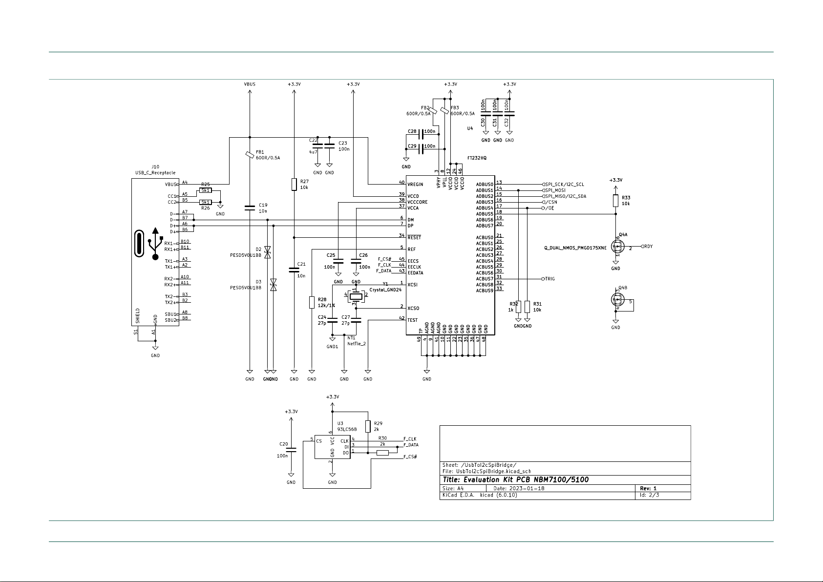
Nexperia UM90022
NBM5100; NBM7100 Evaluation board module
Fig. 15. Schematic (2 of 3)
UM90022 All information provided in this document is subject to legal disclaimers. © Nexperia B.V. 2023. All rights reserved
user manual Rev. 1 — 11 July 2023 16 / 21
Nexperia UM90022
NBM5100; NBM7100 Evaluation board module
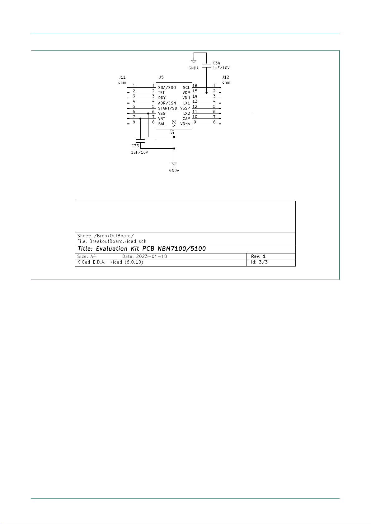
Fig. 16. Schematic (3 of 3)
UM90022 All information provided in this document is subject to legal disclaimers. © Nexperia B.V. 2023. All rights reserved
user manual Rev. 1 — 11 July 2023 17 / 21
Nexperia UM90022
NBM5100; NBM7100 Evaluation board module
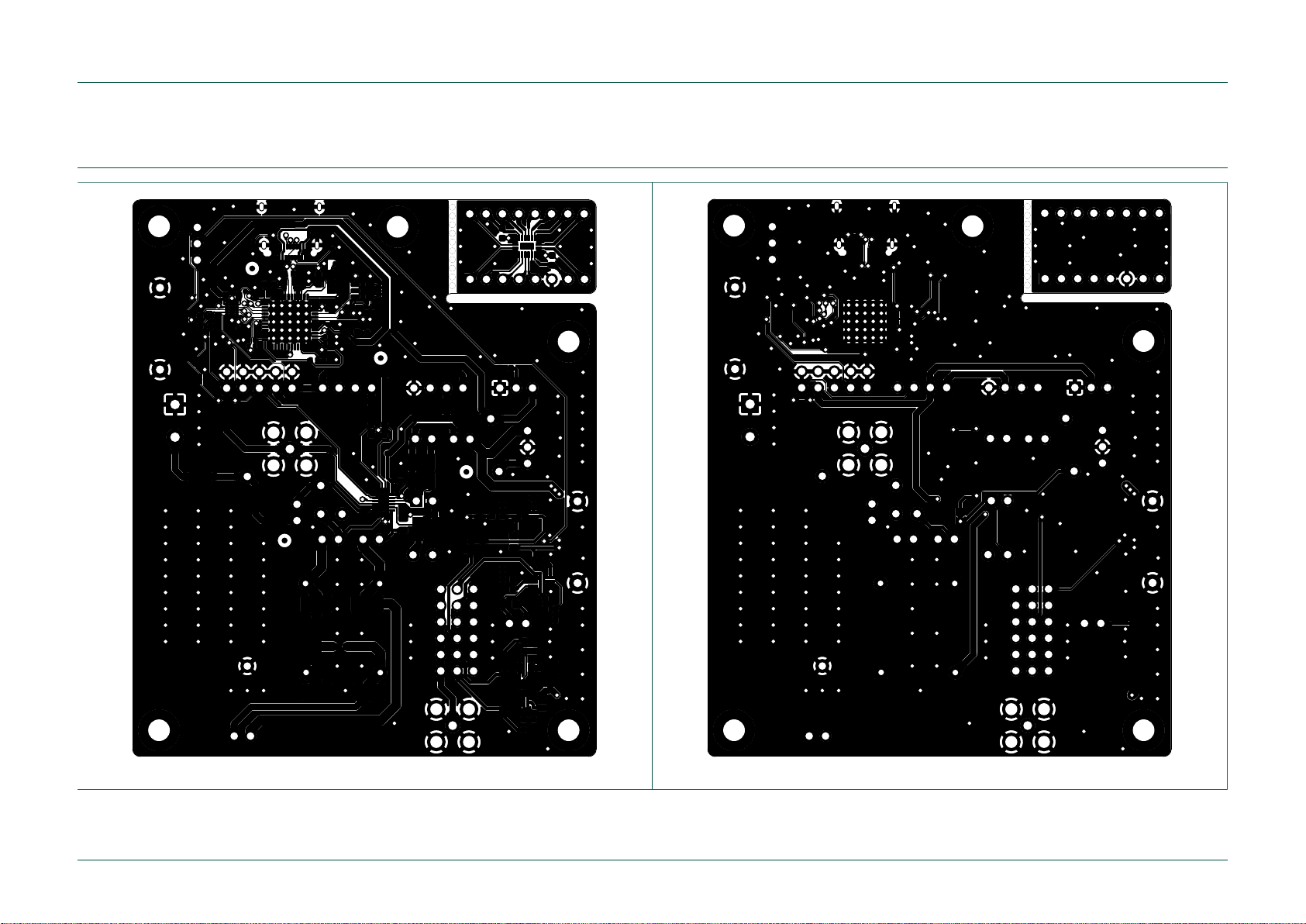
7. Board layout
Fig. 17. Top Side Layer Fig. 18. Bottom Side Layer
UM90022 All information provided in this document is subject to legal disclaimers. © Nexperia B.V. 2023. All rights reserved
user manual Rev. 1 — 11 July 2023 18 / 21

Nexperia UM90022
NBM5100; NBM7100 Evaluation board module
8. Revision history
Table 12. Revision history
Revision
number
Date Description
UM90022 v.1 20230711 Initial version
UM90022 All information provided in this document is subject to legal disclaimers. © Nexperia B.V. 2023. All rights reserved
user manual Rev. 1 — 11 July 2023 19 / 21

Nexperia UM90022
NBM5100; NBM7100 Evaluation board module
9. Legal information
Definitions
Draft — The document is a draft version only. The content is still under
internal review and subject to formal approval, which may result in
modifications or additions. Nexperia does not give any representations or
warranties as to the accuracy or completeness of information included herein
and shall have no liability for the consequences of use of such information.
Disclaimers
Limited warranty and liability — Information in this document is believed
to be accurate and reliable. However, Nexperia does not give any
representations or warranties, expressed or implied, as to the accuracy
or completeness of such information and shall have no liability for the
consequences of use of such information. Nexperia takes no responsibility
for the content in this document if provided by an information source outside
of Nexperia.
In no event shall Nexperia be liable for any indirect, incidental, punitive,
special or consequential damages (including - without limitation - lost
profits, lost savings, business interruption, costs related to the removal
or replacement of any products or rework charges) whether or not such
damages are based on tort (including negligence), warranty, breach of
contract or any other legal theory.
Notwithstanding any damages that customer might incur for any reason
whatsoever, Nexperia’s aggregate and cumulative liability towards customer
for the products described herein shall be limited in accordance with the
Terms and conditions of commercial sale of Nexperia.
Right to make changes — Nexperia reserves the right to make changes
to information published in this document, including without limitation
specifications and product descriptions, at any time and without notice. This
document supersedes and replaces all information supplied prior to the
publication hereof.
Suitability for use — Nexperia products are not designed, authorized or
warranted to be suitable for use in life support, life-critical or safety-critical
systems or equipment, nor in applications where failure or malfunction
of an Nexperia product can reasonably be expected to result in personal
injury, death or severe property or environmental damage. Nexperia and its
suppliers accept no liability for inclusion and/or use of Nexperia products in
such equipment or applications and therefore such inclusion and/or use is at
the customer’s own risk.
Applications — Applications that are described herein for any of these
products are for illustrative purposes only. Nexperia makes no representation
or warranty that such applications will be suitable for the specified use
without further testing or modification.
Customers are responsible for the design and operation of their applications
and products using Nexperia products, and Nexperia accepts no liability for
any assistance with applications or customer product design. It is customer’s
sole responsibility to determine whether the Nexperia product is suitable
and fit for the customer’s applications and products planned, as well as
for the planned application and use of customer’s third party customer(s).
Customers should provide appropriate design and operating safeguards to
minimize the risks associated with their applications and products.
Nexperia does not accept any liability related to any default, damage, costs
or problem which is based on any weakness or default in the customer’s
applications or products, or the application or use by customer’s third party
customer(s). Customer is responsible for doing all necessary testing for the
customer’s applications and products using Nexperia products in order to
avoid a default of the applications and the products or of the application or
use by customer’s third party customer(s). Nexperia does not accept any
liability in this respect.
Export control — This document as well as the item(s) described herein
may be subject to export control regulations. Export might require a prior
authorization from competent authorities.
Translations — A non-English (translated) version of a document is for
reference only. The English version shall prevail in case of any discrepancy
between the translated and English versions.
Trademarks
Notice: All referenced brands, product names, service names and
trademarks are the property of their respective owners.
UM90022 All information provided in this document is subject to legal disclaimers. © Nexperia B.V. 2023. All rights reserved
user manual Rev. 1 — 11 July 2023 20 / 21
This manual suits for next models
5
Table of contents
Other Nexperia Motherboard manuals


