North Coast Synthesis MSK 009 User manual

MSK 009 Coiler Multi-Mode
Filter and Rectifier
North Coast Synthesis Ltd.
Matthew Skala
November 24, 2020

Documentation for the MSK 009
Copyright ©2018, 2019, 2020 Matthew Skala
This documentation is free: you can redistribute it and/or modify it under the terms of the GNU General
Public License as published by the Free Software Foundation, version 3.
This documentation is distributed in the hope that it will be useful, but WITHOUT ANY WARRANTY;
without even the implied warranty of MERCHANTABILITY or FITNESS FOR A PARTICULAR PUR-
POSE. See the GNU General Public License for more details.
You should have received a copy of the GNU General Public License along with this documentation. If not,
see http://www.gnu.org/licenses/.
2

Contents
General notes 5
Controls and connections ......................................... 5
TUNE knob ............................................... 5
res knob ................................................. 5
att knob ................................................. 5
IN inputs ................................................ 6
CV inputs ................................................ 6
HP, BP, and LP outputs ........................................ 6
Specifications ................................................ 6
Voltage modification ............................................ 7
Source package ............................................... 7
PCBs and physical design ......................................... 7
Use and contact information ........................................ 7
Safety and other warnings 9
Bill of materials 10
Building Board 2 12
Preliminaries ................................................ 12
Decoupling capacitors ........................................... 12
Fixed resistors ............................................... 12
Semiconductors ............................................... 14
Electrolytic and film capacitors ...................................... 15
Trimmer potentiometers .......................................... 15
Inductors .................................................. 15
Eurorack power connector ......................................... 16
Building Board 1 17
Preliminaries ................................................ 17
Some notes on knobs ............................................ 17
Decoupling capacitors ........................................... 19
Fixed resistors ............................................... 19
Semiconductors ............................................... 20
Compensation capacitors ......................................... 21
Exponential converter cluster ....................................... 21
Board to board connectors ......................................... 22
Panel components ............................................. 22
Final assembly ............................................... 23
Adjustment and testing 25
Short-circuit test .............................................. 25
Output offset adjustment ......................................... 25
Troubleshooting .............................................. 26
3

Patch ideas 28
Circuit explanation 30
Two-pole state-variable intuition ..................................... 30
Integrators ................................................. 31
Input mixer and rectifier .......................................... 34
Exponential converter ........................................... 35
Mechanical drawings 37
4
General notes
This manual documents the MSK 009 Coiler Multi-
Mode Filter and Rectifier, which is a module for
use in a Eurorack modular synthesizer. The mod-
ule contains a voltage-controlled two-pole state vari-
able filter implemented using inductors (coils, hence
the name) as the main energy-storing components in
the integrators. It also uses capacitors, which have
their main effect at bass frequencies, with the filter’s
behaviour shading from capacitor-based to inductor-
based between about 500Hz to 2kHz. There are sep-
arate outputs for high-pass, band-pass, and low-pass
transfer functions, and two audio inputs, one of which
goes through a full-wave rectifier before being fed into
the filter.
Controls and connections
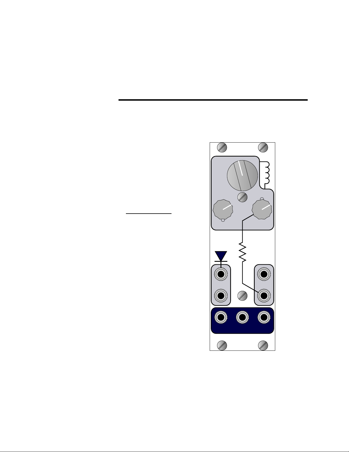
The front panel of the module is shown in Figure 1.
TUNE knob This knob adjusts the overall frequency
of the filter, for all three outputs. Its setting is added
to the control voltage inputs. It should cover the
entire usable range of the filter, with a little bit of
excess at the low end to allow for “closing” the filter
more completely when using voltage control in a low-
pass gate patch.
res knob This sets the “resonance” of the filter by
attenuating one of the feedback paths. Counter-
clockwise for a flatter response curve, clockwise for
a sharper peak. Near the clockwise maximum res-
onance, the filter will oscillate. Because of the way
the inductors respond differently to phase at different
points on the audio spectrum, this knob’s effect inter-
acts with the current frequency setting; the height of
the resonance peak and the point at which oscillation
begins will change with the cutoff frequency, creating
a wide range of varying-timbre effects.
att knob This is an attenuator for the CV2 input—
the lower of the two CV inputs, to which this knob
is joined by the zigzag resistor line in the panel art,
symbolizing attenuation. With the knob fully clock-
wise the sensitivity of this input is approximately
T
U
N
E
res att
fw rect
coiler
multi
mode
filter
IN CV
HP BP LP
MSK 009
NORTH
COAST
Figure 1: Module front panel.
5

1V/octave, the same as the unattenuated input. At
lower settings, the CV2 input is less sensitive.
IN inputs Audio inputs to the filter. The upper in-
put, marked with a diode symbol and the notation fw
rect, is subjected to full-wave rectification (positive
and negative voltages translated into their absolute
values) before being applied to the filter. The lower
input is a direct connection. Both inputs may be used
at once; their effects are summed.
The rectified input includes a phase inverter (both
positive and negative voltages are translated into neg-
ative) to cancel out the naturally-occuring phase in-
version between the input and LP output in this filter
topology. As a result, if you feed an audio signal into
the rectified input with the filter cutoff significantly
below the frequency of the audio, it will be rectified
and filtered into a positive voltage tracking the overall
amplitude of the input signal. This way the module
can be used as an envelope follower.
The inputs can accept any voltages between the
module’s power rails (−12V to +12V) without dam-
age. The module my be overdriven, creating signifi-
cant distortion, with inputs beyond about ±5V.
CV inputs Exponential control voltages for filter
cutoff frequency. The upper socket (CV1) has a
nominal sensitivity of 1V/octave; but the tracking
of this filter is not meant to be very accurate, and
it cannot be made highly accurate because of the
somewhat unpredictable properties of the inductors.
Tracking will differ in different parts of the audio
spectrum. The CV-processing circuit is partially
temperature-compensated, with zeroth-order “offset”
compensation but not first-order “tracking” compen-
sation. The lower socket’s (CV2) sensitivity is ad-
justable with the att knob, to a maximum of the same
sensitivity as CV1. The CV1 input, attenuated CV2
input, and TUNE knob setting are all summed to
produce the control value for the filter core.
Both CV inputs can accept voltages anywhere be-
tween the module’s power rails (−12V to +12V) with-
out damage. Which voltages are useful depends on
the patch and the setting of the TUNE knob, but a
typical user might aim for 0V to 5V.
HP, BP, and LP outputs These are the three out-
puts of the filter core: high-pass, band-pass, and low-
pass. Because this is a two-pole filter, the asymptotic
slopes of the response curves are 12dB/octave for the
high-pass and low-pass, and 6dB/octave on each of
two slopes for the band-pass.
All three outputs are active simultaneously,
driven by the combined input from the two IN jack
sockets. The phase relationships among the three
outputs will change with frequency as the filter shifts
between using its capacitors and its inductors; that
means mixing outputs to produce other filter func-
tions (such as notch filtering) may produce results
that sound good, but they are unlikely to be strong
on measures like stopband attenuation.
Voltage levels on the audio outputs will normally
be similar to the voltage levels on the inputs, with the
maximum possible voltage limited by possible clip-
ping in the op amp chips at around ±10V. Output
level at maximum oscillation will be about ±5V. At
the lowest resonance setting, the BP output will be
a little quieter than the other two, an effect which
tends to disappear at higher resonance.
Specifications
The nominal input impedance is 100kΩfor all inputs
except the rectifier input, which varies between 50kΩ
and 100kΩ. Nominal output impedance is 1kΩfor all
outputs.
Any voltage between the power supply rails (nom-
inally ±12V) is safe for the module, on any input;
output voltages are limited by the capabilities of the
op amps to about ±10V and will clip if the inputs
are driven sufficiently hard. Distortion resulting from
limiting in internal feedback paths may show up be-
fore the outputs actually clip.
The circuit is DC-coupled throughout; as a result,
it can operate at very low frequencies, but small DC
offsets may appear on the outputs. Trimmers are
provided for minimizing offset effects.
Briefly shorting any input or output to any fixed
voltage at or between the power rails, or shorting
two to each other, should be harmless to the module.
Patching the MSK 009’s output into some other mod-
ule’s output should be harmless to the MSK 009, but
doing that is not recommended because it is possible
the non-MSK 009 module may be harmed.
This module (assuming a correct build using the
recommended components) is protected against re-
verse power connection. It will not function with the
power reversed, but will not cause or suffer any dam-
age. Some other kinds of power misconnection may
possibly be dangerous to the module or the power
supply.
In normal operation the maximum current de-
mand of this module is 25mA from the +12V supply
6

and 25mA from the -12V supply. Placing an unusu-
ally heavy load on the outputs (for instance, with so-
called passive modules) can increase the power supply
current beyond those levels.
Voltage modification
This circuit is designed for ±12V power. It should
work acceptably on ±15V power without modifica-
tion, assuming all components are rated for the in-
creased voltage, but some current levels and adjust-
ment ranges are related to the power supplies and so
just applying ±15V power with no changes may not
give optimal results. In particular, I would expect
doing that to create “dead zones” at the ends of the
tuning control range. My suggestion if using ±15V
power would be to increase all four 220kΩresistors
(R5, R8, R19, and R29) to 270kΩ; that should restore
the intended current levels and adjustment ranges.
I have calculated but not tested these resistor
changes.
Source package
A ZIP archive containing source code for this doc-
ument and for the module itself, including things
like machine-readable CAD files, is available from the
Web site at https://northcoastsynthesis.com/.
Be aware that actually building from source requires
some manual steps; Makefiles for GNU Make are pro-
vided, but you may need to manually generate PDFs
from the CAD files for inclusion in the document,
make Gerbers from the PCB design, manually edit
the .csv bill of materials files if you change the bill of
materials, and so on.
Recommended software for use with the source
code includes:
•GNU Make;
•L
A
T
E
X for document compilation;
•LaTeX.mk (Danjean and Legrand, not to be
confused with other similarly-named L
A
T
EX-
automation tools);
•Circuit_macros (for in-document schematic di-
agrams);
•Kicad (electronic design automation);
•Qcad (2D drafting); and
•Perl (for the BOM-generating script).
The kicad-symbols/ subdirectory contains my
customised schematic symbol and PCB footprint li-
braries for Kicad. Kicad doesn’t normally keep de-
pendencies like symbols inside a project directory, so
on my system, these files actually live in a central di-
rectory shared by many projects. As a result, upon
unpacking the ZIP file you may need to do some re-
configuration of the library paths stored inside the
project files, in order to allow the symbols and foot-
prints to be found. Also, this directory will probably
contain some extra bonus symbols and footprints not
actually used by this project, because it’s a copy of
the directory shared with other projects.
The package is covered by the GNU GPL, version
3, a copy of which is included in the file COPYING.
PCBs and physical design
The enclosed PCB design is for two boards. Board
1 is 3.90′′ ×1.50′′ or 99.06mm×38.10mm. Board 2 is
a little shorter, 3.40′′ ×1.50′′ or 86.36mm×38.10mm.
The two boards are intended to mount in a stack par-
allel to the Eurorack panel, held together with M3
machine screws and male-female hex standoff hard-
ware. See Figure 2. Including 18mm of clearance for
the mated power connector, the module should fit in
46mm of depth measured from the back of the front
panel.
Use and contact information
This module design is released under the GNU GPL,
version 3, a copy of which is in the source code pack-
age in the file named COPYING. One important con-
sequence of the license is that if you distribute the
design to others—for instance, as a built hardware
device—then you are obligated to make the source
code available to them at no additional charge, in-
cluding any modifications you may have made to the
original design. Source code for a hardware device in-
cludes without limitation such things as the machine-
readable, human-editable CAD files for the circuit
boards and panels. You also are not permitted to
limit others’ freedoms to redistribute the design and
make further modifications of their own.
I sell this and other modules, both as fully assem-
bled products and do-it-yourself kits, from my Web
storefront at http://northcoastsynthesis.com/.
Your support of my business is what makes it pos-
sible for me to continue releasing module designs for
free. The latest version of this document and the
associated source files can be found at that Web site.
Email should be sent to
7

13mm
stand-
off
11mm
stand-
off
2mm front panel
2×1.6mm PCBs
18mm
clearance
for mated
power
connector
≈46mm depth
Figure 2: Assembled module, side view.
8

Safety and other warnings
Ask an adult to help you.
North Coast Synthesis Ltd. does not offer war-
ranties or technical support on anything we did not
build and sell. That applies both to modules built
by you or others from the kits we sell, and to fully-
assembled modules that might be built by others us-
ing our plans. Especially note that because we pub-
lish detailed plans and we permit third parties to
build and sell modules using our plans subject to the
relevant license terms, it is reasonable to expect that
there will be modules on the new and used markets
closely resembling ours but not built and sold by us.
We may be able to help in authenticating a module
of unknown provenance; contact us if you have ques-
tions of this nature.
For new modules purchased through a reseller,
warranty and technical support issues should be
taken to the reseller first. Resellers buy modules from
North Coast at a significant discount, allowing them
to resell the modules at a profit, and part of the way
they earn that is by taking responsibility for support-
ing their own customers.
We also sell our products to hobbyists who enjoy
tinkering with and customizing electronic equipment.
Modules like ours, even if originally built by us, may
be quite likely to contain third-party “mods,” added
or deleted features, or otherwise differ from the stan-
dard specifications of our assembled modules when
new. Be aware of this possibility when you buy a
used module.
Soldering irons are very hot.
Solder splashes and cut-off bits of component
leads can fly a greater distance and are harder to
clean up than you might expect. Spread out some
newspapers or similar to catch them, and wear eye
protection.
Lead solder is toxic, as are some fluxes used with
lead-free solder. Do not eat, drink, smoke, pick your
nose, or engage in sexual activity while using solder,
and wash your hands when you are done using it.
Solder flux fumes are toxic, especially from lead-
free solder because of its higher working temperature.
Use appropriate ventilation.
Some lead-free solder alloys produce joints that
look “cold” (i.e. defective) even when they are cor-
rectly made. This effect can be especially distressing
to those of us who learned soldering with lead solder
and then switched to lead-free. Learn the behaviour
of whatever alloy you are using, and then trust your
skills.
Water-soluble solder flux must be washed off
promptly (within less than an hour of application)
because if left in place it will corrode the metal. Sol-
der with water-soluble flux should not be used with
stranded wire because it is nearly impossible to re-
move from between the strands.
Residue from traditional rosin-based solder flux
can result in undesired leakage currents that may af-
fect high-impedance circuits. This module does not
use any extremely high impedances, but small leakage
currents could possibly reduce its accuracy. If your
soldering leaves a lot of such residue then it might be
advisable to clean that off.
Voltage and current levels in some synthesizer cir-
cuits may be dangerous.
Do not attempt to make solder flow through the
board and form fillets on both sides of every joint.
Some soldering tutorials claim that that is desirable
or even mandatory, it does look nicer, and it may
happen naturally when the conditions are good and
the leads happen to be small in relation to the holes.
But with large wire leads that just fit in the holes,
when the holes are connected to the ground plane
(even through thermal reliefs), on some harder-to-
wet lead finishes, with lead-free solder, and so on,
you may only end up dumping excessive heat into
the joint and damaging the components while you
fuss over perfect fillets. A well-made solder joint that
just covers the pad and makes good contact to the
lead on one side of the board, is good enough.
Building your own electronic equipment is seldom
cheaper than buying equivalent commercial products,
due to commercial economies of scale from which you
as small-scale home builder cannot benefit. If you
think getting into DIY construction is a way to save
money, you will probably be disappointed.
9

Bill of materials
Qty Ref Value/Part No.
1 C12 33pF radial ceramic, 0.2′′ lead spacing
1 C1 100pF radial ceramic, 0.2′′ lead spacing
2 C2, C3 6800pF film, 0.2′′ lead spacing
6 C6–C11 0.1µF axial ceramic
2 C4, C5 10µF radial aluminum electrolytic, 0.1′′ lead spacing
1 D1 1N4148 or 1N914; switching diode
2 D4, D5 1N5230B 4.7V Zener
2 D2, D3 1N5818 or SB130; Schottky rectifier
2 H1, H2 nut for M3 machine screw
2 H3, H4 M3x11 M3 male-female standoff, 11mm body length
2 H7, H8 M3x13 M3 male-female standoff, 13mm body length
6 H15–H20 M3x6 M3 machine screw, 6mm body length
4 H11–H14 nylon washer for M3 machine screw
7 J1–J7 1502 03 switched mono 3.5mm panel jack, Lumberg
1 J8 female single-row socket, 10 pins at 0.1′′
2 L1, L2 22mH EPCOS 5% axial ferrite choke, B82144A2226J
1 P1 male single-row header, 10 pins at 0.1′′
1 P2 male Eurorack power header, 2×5pins at 0.1′′
2 Q1, Q2 PN200A PNP general purpose amplifier, TO-92 EBC
4 R22, R23, R32,
R33
510Ω
3 R15, R27, R37 1kΩ
1 R6 1.8kΩ
1 R7 2.7kΩ
2 R24, R34 9.1kΩ
2 R25, R35 10kΩ
1 R10 18kΩ
1 R38 22kΩ
4 R21, R26, R31,
R36
27kΩ
1 R11 36kΩ
2 R9, R17 51kΩ
2 R20, R30 100kΩhorizontal single turn, Vishay T73YP or similar
3 R2, R4, R16 100kΩvertical conductive plastic panel pot, BI Technolo-
gies P260T series, linear taper
7 R1, R3,
R12–R14, R18,
R28
100kΩ
4 R5, R8, R19,
R29
220kΩ
10

Qty Ref Value/Part No.
1 U3 LM13700 dual operational transconductance amp
2 U1, U2 TL074 quad JFET-input op amp
Fixed resistors should be 1% metal film throughout. RoHS-certified zinc-plated steel hardware is recom-
mended, not stainless steel because of galvanic-corrosion incompatibility with aluminum parts.
Newer kits may include TL074B op amps instead of TL074, to make offset nulling easier.
Also needed: solder and related supplies, PCB, panel, knobs, a cable tie, Eurorack power cable, etc.
11
Building Board 2
The recommended order for building this module is
to assemble Board 2, the one further from the front
panel, first. That will make it easier to get all the
physical positioning right for the components that
bridge between the boards or pass through the panel.
Note that although I’m describing a separate step
for each component value, and that’s how I built my
prototype so as to have plenty of photo opportunities,
if you are reasonably confident about your skills you
may find it easier to populate all or most of the board
(i.e. put the components in place) and then solder
them in a single step. Except where noted, the order
in which you add components does not matter much.
Preliminaries
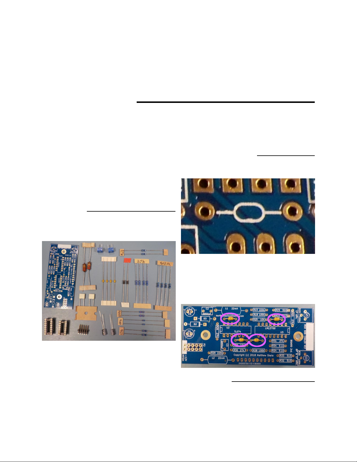
Count out the right number of everything according
to the bill of materials. There is an abbreviated BOM
for Board 2, excluding a few items that will be added
when combining this board with Board 1, in Table 2.
There are two trimmers to be installed on this
board. Before installing them, use an ohmmeter to
adjust each one to 50% of its range. Measure the re-
sistance along the track, then measure the resistance
from the wiper to one end and adjust to make the
wiper half the total track resistance. This need not
be exact, but having them start near their midpoints
will help with adjustment later, by reducing issues
with interaction among the different settings. With
both trimmers pre-set to 50%, the module should ba-
sically work even if it is not at its best, whereas if
they are installed at extreme values instead, then you
may have trouble getting it up and running enough
to adjust it more accurately.
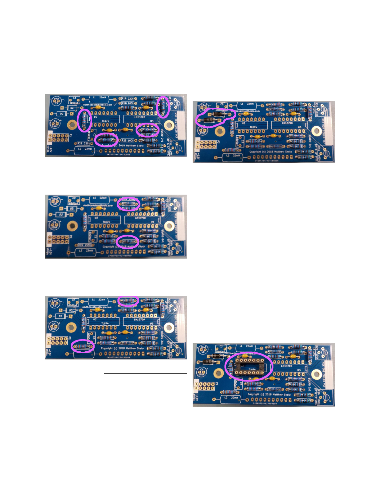
Decoupling capacitors
The four axial ceramic 0.1µF decoupling capacitors,
C8 to C11, are shown on the board by a special sym-
bol without their reference designators.
Install these four capacitors where the symbol ap-
pears. They are not polarized and may be installed
in either orientation. These capacitors act as filters
for the power supplies to the op amp and OTA chips.
An MSK 009 kit should include six of these capaci-
tors, and only four are used on this board; save the
remaining two for use on Board 1.
Fixed resistors
Resistors are never polarized. I like to install mine in
a consistent direction for cosmetic reasons, but this
is electrically unnecessary. In this module, the fixed
12

Qty Ref Value/Part No.
2 C2, C3 6800pF film, 0.2′′ lead spacing
4 C8–C11 0.1µF axial ceramic
2 C4, C5 10µF radial aluminum electrolytic, 0.1′′ lead spacing
2 D2, D3 1N5818 or SB130; Schottky rectifier
2 L1, L2 22mH EPCOS 5% axial ferrite choke, B82144A2226J
1 P2 male Eurorack power header, 2×5pins at 0.1′′
4 R22, R23, R32, R33 510Ω
2 R24, R34 9.1kΩ
2 R25, R35 10kΩ
4 R21, R26, R31, R36 27kΩ
2 R20, R30 100kΩhorizontal single turn, Vishay T73YP or similar
2 R18, R28 100kΩ
2 R19, R29 220kΩ
1 U2 14-pin DIP socket
1 U3 16-pin DIP socket
Table 2: Bill of Materials for assembling Board 2. Also needed is the PCB itself.
resistors are metal film 1% type. They usually have
blue bodies and four colour bands designating the
value, plus a fifth band for the tolerance. The tol-
erance band is brown for 1%, but note that we may
occasionally ship better-tolerance resistors in the kits
than the specifications require, if we are able to source
them at a good price. Accordingly, I mention only the
four value band colours for this type of resistor; if you
are using resistors with other codes, you are respon-
sible for knowing them. Note that colour codes on
metal film 1% resistors are often ambiguous (reading
from one end or the other end may give two different
values, both plausible) and some of the colours are
hard to distinguish anyway. If in doubt, always mea-
sure with an ohmmeter before soldering the resistor
in place.
Install the four 510Ω(green-brown-black-black)
resistors R22, R23, R32, and R33. These resistors,
with the 100kΩones added later, set the signal levels
at the inputs of the OTA chips.
Install the two 9.1kΩ(white-brown-black-brown)
resistors R24 and R34. These limit the maximum
control current for the OTAs.
Install the two 10kΩ(brown-black-black-red) re-
sistors R25 and R35. These are feedback resistors for
the current-to-voltage converters in the filter core.
13
Install the four 27kΩ(red-violet-black-red) resis-
tors R21, R26, R31, and R36. These are feedback
resistors for the integrators (R26 and R36), and set
the current for the linearizing diodes in the LM13700
chips (R1 and R31).
Install the two 100kΩ(brown-black-black-orange)
resistors R18 and R28. These resistors participate in
setting the input levels for the OTA chips. A full
kit contains seven resistors of this value; five should
remain for use on Board 1.
Install the two 220kΩ(red-red-black-orange) re-
sistors R19 and R29. These resistors set the adjust-
ment ranges for the DC offset trimmers. A full kit
contains four resistors of this value; save two for use
on Board 1.
Semiconductors
Install the two 1N5818 or SBA130 Schottky rectifier
diodes D2 and D3. These are for reverse-voltage pro-
tection; they cut off power to the module when the
power plug is backwards. They are polarized and it is
important to install them in the right direction. Each
diode is packaged inside a black or dark grey plastic
slug with a white or light grey stripe at one end;
that end is the cathode. The silkscreen markings on
the board have a corresponding stripe and the diodes
should be installed with their stripes matching the
markings on the board. The solder pads for the cath-
odes are also square instead of round. Installing these
backwards means they will have the opposite of the
intended protective effect.
Install the 14-pin DIP socket for the operational
amplifier chip U2. This chip does most of the am-
plification in the filter core. DIP sockets themselves
do not care which direction you install them, but it
is critically important that the chips installed in the
sockets should be installed in the right direction. To
help with that, the sockets will probably be marked
with notches at one end (indicating the end where
Pin 1 and Pin 14 are located) and you should in-
stall the sockets so that the notched ends match the
notches shown on the PCB silkscreen. The solder pad
for Pin 1 is also distinguished by being rectangular
instead of rounded.
Installing DIP sockets without having them tilted
at a funny angle can be tricky. I recommend inserting
the socket in the board, taping it in place on the
component side with vinyl electrical tape or sticking
it there with a small blob of putty at each end, then
soldering one pin on one corner and checking that
the socket is snug against the board before soldering
the other pins. That way, if you accidentally solder
the first pin with the socket tilted, it will be easier
to correct (only one pin to desolder instead of all of
them).
If you somehow manage to solder an entire socket
in backwards, don’t try to desolder it to turn it
around. Just leave it as it is and remember that when
14

you insert the chip, you must insert it so the chip
matches the markings on the board, not the turned-
around socket.
Install the 16-pin DIP socket for the OTA (opera-
tional transconductance amplifier) chip U3. This chip
contains two current-controlled amplifiers, which, by
means of a frequency-dependent control current, tune
the filter core to the desired frequency. See the gen-
eral instructions regarding DIP sockets above.
Electrolytic and film capacitors
Install the two 6800pF film capacitors C2 and C3.
These are timing components used in the integrators
at low frequencies to complement the inductors used
at medium to high frequencies. They are unpolarized
components and may be installed in either orienta-
tion.
The markings on film capacitors may vary de-
pending on the manufacturer and model. These ones
might be marked “682” (for 68 followed by two 0s
number of picofarads), “6n8” (for 6.8nF), or even
“0.0068” (value in µF). However, these are the only
film capacitors in the module, so confusion is unlikely.
Install the two 10µF electrolytic capacitors C4
and C5, which filter the power supply for the mod-
ule as a whole. These are polarized components and
they may explode if installed backwards. Each one
will be marked on its casing with a stripe and minus
signs to indicate the negative lead; the positive lead
will probably also be longer. These clues should be
matched with the markings on the PCB: plus and
minus symbols in the silkscreen and a square solder
pad for the positive (long) lead.
Trimmer potentiometers
If you have not already set the trimmers to 50% of
their full scale value as described under “Preliminar-
ies” above, then do it now.
Trimmers usually are not washable, so if you plan
to clean your boards by full immersion in water or
other solvent, your last chance is now; future clean-
ing will have to be done with a brush and some care
to avoid letting liquid seep into the trimmers. Even
now you should take some care with the DIP sockets,
because solvent can carry flux residue into them and
form a varnish-like layer if not carefully rinsed away.
Trimmers are not exactly polarized, but the three
legs of each trimmer serve different functions and
need to be connected to the right holes. The physi-
cal arrangement of the legs and corresponding holes
should make it impossible to install the trimmers
wrong way round.
Install the two 100kΩtrimmers R20 and R30.
These trimmers are for compensating DC offsets in
the filter core.
Inductors
The two 22mH ferrite-bobbin inductors, that is, coils,
L1 and L2 give this module its name. Install them
now. They are the main timing components in the
filter core, serving at medium to high frequencies.
Single inductors like these have no polarity and may
be installed in either direction; the situation is more
complicated with transformers made of two or more
interacting inductors.
15

The inductors are delicate, especially in the area
where the leads attach to the bodies, because the
windings that connect to the leads are made of very
fine wire. The ferrite core material is also somewhat
brittile. It is important not to bend the leads too
close to the bodies. There is some extra space for the
inductors on the circuit board to allow for a gentle
bend radius.
Eurorack power connector
Install the 2×5-pin Eurorack power connector J2.
This connector is not polarized in itself, although
the connection it makes is polarized. As with the
DIP sockets, you should be careful to get it installed
snugly against the board, not tilted at an angle. Use
tape or putty to hold it in place, solder one pin, then
check that it is straight before you solder the other
pins.
The six pins in the centre of the connector, that is
all except the four corner pins, are for grounding and
they are all connected together on the board. Thus, if
you accidentally form solder bridges among these six
pins while installing the connector, don’t waste effort
trying to remove them; they will have no electrical
effect.
In between completed boards is a good time to
take a break.
16

Building Board 1
Board 1 has components on both sides, and for best
results, it is important to install them in the right
order. Build Board 2 first, and see the general com-
ments in the Board 2 chapters about how to approach
the task.
Preliminaries
Count out the right number of everything according
to the bill of materials. There is an abbreviated BOM
for the items needed in this chapter (including the
connection to Board 2 and final assembly of the mod-
ule) in Table 3.
Some notes on knobs
The first batch of knobs I ordered for North Coast
products turned out to have serious quality problems,
specifically with the setscrews that hold the knobs
onto the potentiometer shafts. Some of the screws
had marginal threads that would strip when the screw
was tightened, and I ended up having to do a bunch of
extra testing and ship extra knobs to some customers
to replace any that might fail. Later batches have
also had issues, although they’re under better control
now because the bad first batch served as a warning
to step up the testing procedures. Starting with kits
prepared in August 2019, I switched to blue knobs
with 100% testing; in September 2020, I switched to
a new manufacturer, and knobs that are a slightly
darker shade of blue. Although all the knobs I ship
in kits now have been tested and passed at least twice,
and should be fine to use, I am also shipping spare
setscrews in any kits with knobs from batches where
a signficant number of knobs failed testing.
Here are some things to be aware of as a kit
builder.
•Some photos in these instructions were taken
with the older grey knobs, and some dealers
will still have kits containing grey knobs in their
stock, but newer kits will have blue knobs.
•Do not overtighten the setscrews when attach-
ing the knobs! The screw should be tight
enough to hold the knob onto the shaft, but
there’s no advantage to making it tighter than
that, and overtightening may risk destroying
the screw thread or damaging the drive slot.
•If, despite my efforts to make sure no bad screws
get sent to customers, you still get a bad screw
that cannot be tightened and no spare for it,
then please contact me.
•If you want to source an exact replacement for
the setscrew, it should be an M3×3mm flat-tip
slotted setscrew, which is also sometimes called
a “grub screw,” made of RoHS-compliant brass
(possibly by exemption). Stainless steel is fine
too, and I may sometimes ship stainless steel
screws instead of brass if I can find a reliable
source for them; plain steel should not be used
here for galvanic corrosion reasons. Hex-socket
screws are fine if you have the driver for them,
but I don’t ship those because I’m not sure all
DIY builders do have the right driver.
•Because it’s a standard M3 thread, in a pinch
it’s possible to substitute a plain M3 machine
screw such as are commonly used with Eurorack
cases, although one of those would obviously
look less nice.
17

Qty Ref Value/Part No.
1 C12 33pF radial ceramic, 0.2′′ lead spacing
1 C1 100pF radial ceramic, 0.2′′ lead spacing
2 C6, C7 0.1µF axial ceramic
1 D1 1N4148 or 1N914; switching diode
2 D4, D5 1N5230B 4.7V Zener
2 H1, H2 nut for M3 machine screw
2 H3, H4 M3x11 M3 male-female standoff, 11mm body length
2 H7, H8 M3x13 M3 male-female standoff, 13mm body length
2 H15, H16 M3x6 M3 machine screw, 6mm body length
7 J1–J7 1502 03 switched mono 3.5mm panel jack, Lumberg
1 J8 female single-row socket, 10 pins at 0.1′′
1 P1 male single-row header, 10 pins at 0.1′′
2 Q1, Q2 PN200A PNP general purpose amplifier, TO-92 EBC
3 R15, R27, R37 1kΩ
1 R6 1.8kΩ
1 R7 2.7kΩ
1 R10 18kΩ
1 R38 22kΩ
1 R11 36kΩ
2 R9, R17 51kΩ
3 R2, R4, R16 100kΩvertical conductive plastic panel pot, BI Technolo-
gies P260T series, linear taper
5 R1, R3, R12–R14 100kΩ
2 R5, R8 220kΩ
1 U3 LM13700 dual operational transconductance amp
2 U1, U2 TL074 quad JFET-input op amp
1 U1 14-pin DIP socket
Table 3: Bill of Materials for Board 1. Newer kits may include TL074B op amps instead of TL074, to
make offset nulling easier. Also needed: the PCB itself, the aluminum front panel, knobs, a cable tie, the
assembled Board 2, and panel-to-rack mounting hardware.
18
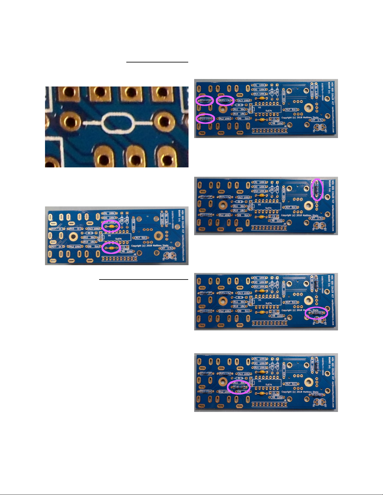
Decoupling capacitors
The two axial ceramic 0.1µF decoupling capacitors
C6 and C7 are shown on the board by a special sym-
bol without their reference designators.
Install these two capacitors where the symbol ap-
pears. They are not polarized and may be installed
in either orientation. These capacitors act as filters
for the power supplies to the op amp chip, protecting
them from high-frequency crosstalk.
Fixed resistors
Resistors are never polarized. I like to install mine in
a consistent direction for cosmetic reasons, but this
is electrically unnecessary. In this module, the fixed
resistors are metal film 1% type. They usually have
blue bodies and four colour bands designating the
value, plus a fifth band for the tolerance. The tol-
erance band is brown for 1%, but note that we may
occasionally ship better-tolerance resistors in the kits
than the specifications require, if we are able to source
them at a good price. Accordingly, I mention only the
four value band colours for this type of resistor; if you
are using resistors with other codes, you are respon-
sible for knowing them. Note that colour codes on
metal film 1% resistors are often ambiguous (reading
from one end or the other end may give two different
values, both plausible) and some of the colours are
hard to distinguish anyway. If in doubt, always mea-
sure with an ohmmeter before soldering the resistor
in place.
Install the three 1kΩ(brown-black-black-brown)
resistors R15, R27, and R37. These are current-
limiting resistors to protect the audio outputs, and
other modules, in case of short circuits or bad patch-
ing.
Install the 1.8kΩ(brown-grey-black-brown) resis-
tor R6. This is the feedback resistor for the CV-
processing op amp, setting the CV sensitivity to ap-
proximately 1V/octave. Do not confuse this with the
18kΩresistor, which has a similar colour code.
Install the 2.7kΩ(red-violet-black-brown) resistor
R7. This is a ballast resistor for the temperature-
servo op amp, preventing the voltage gain of the tran-
sistor in the feedback loop from rendering the ampli-
fier unstable.
Install the 18kΩ(brown-grey-black-red) resistor
R10. This resistor is used to control the gain in the
full-wave rectifier circuit.
Install the 22kΩ(red-red-black-red) resistor R38.
This resistor controls the amount of clipping applied
on an internal feedback path, to set the amplitude
19

level during oscillation. Do not confuse this resistor
with the 220kΩresistors, which have a similar colour
code.
Install the 36kΩ(orange-blue-black-red) resistor
R11. This controls the level of the full-wave rectified
input signal applied to the input mixer.
Install the two 51kΩ(green-brown-black-red) re-
sistors R9 and R17. These are used for level and
impedance control: R9 on the rectifier input, and
R17 on the internal BP feedback path.
Install the five 100kΩ(brown-black-black-orance)
resistors R1, R3, R12, R13, and R14. The first three
of these are used to set input impedances for the un-
rectified audio input and both CV inputs. The re-
maining two, R13 and R14, set gain levels in the in-
put mixer.
Install the two 220kΩ(red-red-black-orange) re-
sistors R5 and R8. The first, R5, controls the scale
of the main tuning knob; the second, R8, contols the
reference current for the exponential converter.
Semiconductors
There are two different kinds of diodes to install on
this board and they look almost exactly alike: one
1N4148 or 1N914 switching diode named D1, and two
1N5230B or equivalent 4.7V Zener diodes named D4
and D5. All three diodes will be packaged in little
pink glass beads with near-microscopic etched num-
bers indicating their type. Be careful not to confuse
them; swapping the switching diode with a Zener will
result in incorrect behaviour of the full-wave rectifier
at high input voltages, and incorrect feedback levels
probably causing either very strong oscillation at all
resonance settings, or preventing oscillation entirely.
If you are unsure which diode is which and you
cannot confidently read the etched markings, hook up
a diode in series with a 10kΩresistor reverse-biased
across a 12V power supply and measure the voltage
drop across the diode. If it is near 12V, then you are
testing the switching diode; if it is near 4.7V, you are
testing one of the Zener diodes; if it is near 0.6V, you
probably have the diode connected forward-biased
and should reverse the polarity of it or the power
supply.
Both kinds of diodes are polarized and must be
installed in the correct direction to function properly.
One end of the glass body of the diode package will
be labelled with a black band or stripe; that end is
the cathode. The direction for the cathode is marked
on the PCB silkscreen by a matching stripe in the
printed symbol; and the solder pad for the cathode is
square rather than round. The note “4.7V” is also on
the PCB silkscreen next to the locations of the two
Zener diodes as an added reminder of which diode
goes where.
20
Table of contents


