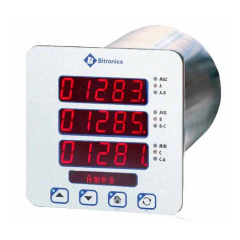
Novatech Bitronics M87X Series User manual

M87X SERIES MEASUREMENT SYSTEM
Monitoring and Recording IED Manual
August 15, 2018
ML0021 Document Revision R
© 2018 by Bitronics, LLC


ML0021 August 15, 2018 ii Copyright 2018 Bitronics, LLC
TABLE OF CONTENTS
FIRMWARE VERSION.....................................................................................................................................vii
M87x MANUAL SET .........................................................................................................................................ix
INSTALLATION AND MAINTENANCE.............................................................................................................x
WARRANTY AND ASSISTANCE......................................................................................................................x
AUTHORIZED REPRESENTATIVE IN THE EUROPEAN UNION ..................................................................xi
COPYRIGHT NOTICE.......................................................................................................................................xi
TRADEMARKS .................................................................................................................................................xi
SAFETY SECTION..........................................................................................................................................xiii
1.0 DESCRIPTION ............................................................................................................................................1
1.1 Introduction..............................................................................................................................................1
1.2 Features ..................................................................................................................................................1
1.3 Specifications ..........................................................................................................................................1
1.4 Standards and Certifications .................................................................................................................10
1.4.1 Revenue Accuracy.........................................................................................................................10
1.4.2 Environment...................................................................................................................................10
2.0 HOUSING AND BACKPLANE .................................................................................................................15
2.1 Installation .............................................................................................................................................18
2.2 Initial Inspection.....................................................................................................................................18
2.3 Protective Ground/Earth Connections...................................................................................................18
2.4 Instrument Mounting..............................................................................................................................18
2.5 Surge Protection....................................................................................................................................18
2.6 Cleaning ................................................................................................................................................18
2.7 Removal and Installation of Modules ....................................................................................................19
3.0 HOST / ANALOG-DIGITAL SIGNAL PROCESSOR MODULE H11/H12 AND A10...............................20
3.1 Host board.............................................................................................................................................20
3.1.1 Serial Port/Front Panel Board ........................................................................................................20
3.1.1a Service Port (P1) .....................................................................................................................20
3.1.1b Standard Serial Ports (P2, P3, P4)..........................................................................................21
3.1.1c Diagnostic Status LED’s (S1, S2, S3, S4) ...............................................................................22
3.1.1d RS485 Connections.................................................................................................................22
3.1.2 Self-Test Modes .............................................................................................................................31
3.1.3 System Clock .................................................................................................................................32
3.2 A10 Analog-Digital Signal Processor Board .........................................................................................32
3.2.1 Calibration ......................................................................................................................................32
3.2.2 Instantaneous Measurement Principles.........................................................................................32
3.2.2a Sampling Rate and System Frequency...................................................................................32
4.0 MEASUREMENTS ....................................................................................................................................33
4.1 Current (1/4-Cycle Update) ...................................................................................................................33
4.1.1 Neutral and Residual Current (1/4-Cycle Update) .........................................................................33
4.2 Voltage Channels (1/4-Cycle Update)...................................................................................................33
4.3 Power Factor (1-Cycle Update).............................................................................................................34
4.4 Watts / Volt-Amperes (VAs) / VARs (1-Cycle Update)..........................................................................34
4.4.1 Geometric VA Calculations ............................................................................................................35
4.4.2 Arithmetic VA Calculations.............................................................................................................35
4.4.3 Equivalent VA Calculations............................................................................................................36

ML0021 August 15, 2018 iii Copyright 2018 Bitronics, LLC
4.5 Energy (1-Cycle Update).......................................................................................................................36
4.6 Frequency (1-Cycle Update) .................................................................................................................37
4.7 Demand Measurements (1-Second Update) ........................................................................................37
4.7.1 Ampere and Fundamental Ampere Demand .................................................................................38
4.7.2 Volt Demand ..................................................................................................................................38
4.7.3 Power Demands (Total Watts, VARs, and VAs)............................................................................39
4.7.4 Voltage THD Demand....................................................................................................................39
4.7.5 Current TDD Demand ....................................................................................................................39
4.7.6 Demand Resets .............................................................................................................................39
4.7.7 Demand Interval.............................................................................................................................39
4.8 Harmonic Measurements (1-Cycle Update)..........................................................................................40
4.8.1 Voltage Distortion (THD) (1-Cycle Update) ...................................................................................40
4.8.2 Current Distortion (THD and TDD) (1-Cycle Update) ....................................................................40
4.8.3 Fundamental Current (1-Cycle Update).........................................................................................41
4.8.4 Fundamental Neutral Current (M871 Only) (1-Cycle Update) .......................................................41
4.8.5 Fundamental Voltage (1-Cycle Update) ........................................................................................41
4.8.6 Fundamental Watts / Volt-Amperes (VAs) / VARs (1-Cycle Update) ............................................42
4.8.7 K-Factor (1-Cycle Update) .............................................................................................................42
4.8.8 Displacement Power Factor (1-Cycle Update) ..............................................................................42
4.8.9 Phase Angle (1-Cycle Update) ......................................................................................................42
4.8.10 Resistance, Reactance, Impedance (1-Cycle Update)................................................................43
4.8.11 Slip Frequency (1-Cycle Update).................................................................................................43
4.8.12 Individual Phase Harmonic Magnitudes and Phase Angles (1-Cycle Update)............................43
4.9 Temperature (1-Second Update) ..........................................................................................................43
4.10 Symmetrical Components (1-Cycle Update) .....................................................................................43
4.11 Supply Voltage and Current Unbalance (1-Cycle Update) ................................................................43
4.12 Flicker..................................................................................................................................................44
4.13 Fault Analysis ......................................................................................................................................44
4.13.1 Line Parameters...........................................................................................................................44
4.13.2 Peak Current................................................................................................................................44
4.13.3 Status Indication and Reset .........................................................................................................44
4.13.4 SOELOG Output ..........................................................................................................................45
4.13.5 Protocol Output ............................................................................................................................45
4.14 List of Available Measurements ..........................................................................................................47
5.0 FUNCTIONAL DESCRIPTION..................................................................................................................50
5.1 Passwords.............................................................................................................................................50
5.2 Configuration .........................................................................................................................................50
5.3 Triggering ..............................................................................................................................................52
5.3.1 Threshold Trigger...........................................................................................................................52
5.3.1a Trigger Hysteresis....................................................................................................................52
5.3.2 Digital Input Trigger........................................................................................................................54
5.3.3 Edge and Level Triggers................................................................................................................54
5.3.4 Manual Trigger...............................................................................................................................55
5.3.5 Logical Combinations of Triggers ..................................................................................................55
5.3.6 Cross Triggering Multiple 70 Series Units (Inter-triggering) ..........................................................55
5.3.7 Fault Distance Triggers..................................................................................................................55
5.3.8 Periodic Triggers............................................................................................................................56
5.4 Recording ..............................................................................................................................................57
5.4.1 Waveform Recorder.......................................................................................................................57
5.4.1a Default Frequency Setting for Waveform Recorder ................................................................59
5.4.1b Indicating Waveform Records with Digital Outputs .................................................................59
5.4.1c Retrieving and Deleting Waveform Recorder Files .................................................................60
5.4.2 Disturbance Recorders ..................................................................................................................60
5.4.2a Indicating Disturbance Records with Digital Outputs ..............................................................61
5.4.2b Retrieving and Deleting Disturbance Recorder Files ..............................................................61
5.4.3 Trend Recorder ..............................................................................................................................62
5.4.3a Retrieving Trend Records........................................................................................................62
5.4.4 Comtrade Format ...........................................................................................................................62
5.4.4a Comtrade ZIP Files...................................................................................................................63

ML0021 August 15, 2018 iv Copyright 2018 Bitronics, LLC
5.4.5 IEEE Long File Naming Convention ...............................................................................................63
5.4.6 Voltage Fluctuation Table (VFT) File ..............................................................................................65
5.4.7 Sequence of Events (SOE) File......................................................................................................67
5.4.8 Sequence of Events Recorder (SER) File ......................................................................................67
5.5 M87x File System..................................................................................................................................68
5.5.1 FTP Server.....................................................................................................................................68
5.5.1a Introduction to FTP ..................................................................................................................69
5.5.1b M87x FTP Implementation ......................................................................................................69
5.5.2 Zmodem, TELNET, and Command Line Interface ........................................................................70
5.6 Assigning Pulse Outputs to Energy Values ..........................................................................................71
5.7 IRIG-B ...................................................................................................................................................71
5.7.1 Overview ........................................................................................................................................71
5.7.2 Introduction to IRIG Standards ......................................................................................................72
5.7.2a Time Code Format (Rate Generation).....................................................................................72
5.7.2b Format Designation .................................................................................................................72
5.7.2c Carrier/Resolution ....................................................................................................................73
5.7.2d Coded Expressions..................................................................................................................73
5.7.3 M87x IRIG-B Implementation.........................................................................................................73
5.7.3a M87x IRIG-B Receiver.............................................................................................................73
5.7.3b M87x IRIG-B Decoder .............................................................................................................73
5.7.3c M87x IRIG-B Time Qualifier.....................................................................................................74
5.7.4 Determining the Correct Year ........................................................................................................74
5.7.5 Methods of Automatic Clock Adjustments .....................................................................................75
5.7.6 Types of M87x Clock Synchronization...........................................................................................75
5.7.6a Frequency Adjustments and Free Wheeling ...........................................................................75
5.7.6b Permanent IRIG-B Source Connection ...................................................................................76
5.7.7 Stages of IRIG-B Synchronization and Accuracy ..........................................................................76
5.7.7a Power-Up Stage ......................................................................................................................76
5.7.7b Time Lock Stage......................................................................................................................76
5.7.7c Frequency Lock Stage.............................................................................................................77
5.7.7d Final Lock Stage......................................................................................................................77
5.7.8 Notes On Operation .......................................................................................................................77
5.7.9 IRIG-B Electrical Specifications .....................................................................................................77
5.7.10 IRIG-B Port Wiring Instructions (Pulse Width Coded, IRIG-B master, .........................................77
Demodulated)...........................................................................................................................................77
5.7.11 Modulated IRIG-B .........................................................................................................................78
5.7.12 Setup Instructions for Use of the M87x Modulated IRIG-B Converter (Sine ................................78
Wave, Amplitude Modulated, IRIG-B master)..........................................................................................78
5.8 Time Sync & Setting.............................................................................................................................79
5.8.1 Time Sync Status Registers.........................................................................................................79
5.8.2Manual time setting by Command-Line instruction.....................................................................79
5.8.3Unsolicited DNP Time set (DNP master sets the IED clock)......................................................79
5.8.4IRIG-B Time sync (time-synchronization via dedicated IED port) ..............................................79
5.8.5(UCA) Network Time Synchronization - time synchronization over Ethernet .............................80
5.8.6SNTP (Simple Network Time Protocol) - time synchronization over Ethernet ...........................80
5.8.7DNP Time sync (slave requesting DNP time be set) ..................................................................80
5.9 Using the M87x with a Bitronics Analog Output Converter...................................................................81
5.10 Automatic Event Notification ...............................................................................................................81
5.10.1 Email Notifications .......................................................................................................................81
5.10.2 Serial Notifications .......................................................................................................................81
5.10.3 Data Sent .....................................................................................................................................81
5.10.4 Error Recovery .............................................................................................................................82
5.10.5 Example .......................................................................................................................................82
5.10.6 Control Characters........................................................................................................................82
6.0 POWER SUPPLY V10 ..............................................................................................................................83
6.1 Introduction............................................................................................................................................83
6.2 Features ................................................................................................................................................83
6.3 Specifications ........................................................................................................................................83
6.3.1 Environmental ................................................................................................................................84

ML0021 August 15, 2018 vCopyright 2018 Bitronics, LLC
6.3.2 Physical..........................................................................................................................................84
6.4 Power Supply and Protective Ground (Earth) Connections..................................................................85
6.5 Overcurrent Protection ..........................................................................................................................85
6.6 Supply/Mains Disconnect......................................................................................................................85
7.0 SIGNAL INPUT MODULE S10 - S12, S1C (M871), S13 - S17, S2C (M872) ..........................................86
7.1 Introduction............................................................................................................................................86
7.2 Features ................................................................................................................................................86
7.3 Specifications ........................................................................................................................................87
7.4 Current Input (CT) Connections ............................................................................................................93
7.5 Voltage Input (VT) Connections ............................................................................................................94
7.5.1 Overcurrent protection for Voltage input (VT) Connections...........................................................94
7.6 Current Measurements..........................................................................................................................95
7.6.1 Neutral Current (Residual Current) for WYE Connections ............................................................95
7.7 Voltage Measurements .........................................................................................................................95
7.8 Changing Transformer Ratios ...............................................................................................................95
7.9 User (External Transformer) Gain and Phase Correction.....................................................................95
7.10 Calibration ...........................................................................................................................................96
7.11 Installation and Calibration for the S1C Option...................................................................................96
8.0 ETHERNET MODULE P10, P11, P12 OR E1, E3 OPTION WITH H12 HOST......................................108
8.1 Introduction..........................................................................................................................................108
8.2 Features ..............................................................................................................................................109
8.3 Specifications (For P1x Modules Unless Otherwise Noted) ...............................................................109
8.4 Environmental .....................................................................................................................................110
8.5 Physical ...............................................................................................................................................110
8.6 Hot Swap (HS) Compatibility (P1x Modules) ......................................................................................110
8.7 Hardware Configuration ......................................................................................................................110
8.8 Cabling ................................................................................................................................................111
8.9 Connections ........................................................................................................................................111
8.10 Troubleshooting the Connection .......................................................................................................111
8.11 Indicators...........................................................................................................................................111
8.12 Software Configuration......................................................................................................................112
8.13 Technical Details ...............................................................................................................................112
8.13.1 Jumper Settings (P1x) ...............................................................................................................114
8.13.2 Troubleshooting .........................................................................................................................115
8.13.3 PHYSTS Register Contents (P1x) .............................................................................................116
8.13.4 Statistics Gathered by Ethernet Driver ......................................................................................117
9.0 DIGITAL INPUT / OUTPUT MODULE P30A, P31, P33.........................................................................118
9.1 Introduction..........................................................................................................................................118
9.2 Features ..............................................................................................................................................118
9.3 Specifications ......................................................................................................................................119
9.4 Environmental .....................................................................................................................................120
9.5 Physical ...............................................................................................................................................120
9.6 Hot Swap (HS) Compatibility...............................................................................................................120
9.7 Description ...........................................................................................................................................120
9.7.1 P30A .............................................................................................................................................120
9.7.2 P31...............................................................................................................................................121
9.7.3 P33...............................................................................................................................................121
9.8 System Design Considerations ...........................................................................................................121
9.8.1 Input / Output Impedance .............................................................................................................121
9.8.2 Input Assignments .......................................................................................................................121
9.9 Debounce Time Setting.......................................................................................................................122
9.10 Setting Digital I/O Module Jumpers...................................................................................................125
9.10.1 Disassembly of the P30A Module..............................................................................................125
9.10.2 Disassembly of the P31 Module ................................................................................................125
9.10.3 CompactPCITM Interface Board (692) Jumper Settings.............................................................126
9.10.4 I/O Board (693) Jumper Settings ...............................................................................................127
9.10.5 Health Status Digital Output Setting (Optional assignment of Digital Output 1 of Module 0)....129

ML0021 August 15, 2018 vi Copyright 2018 Bitronics, LLC
9.10.6 Disassembly of the P33 Module ................................................................................................129
9.10.7 Digital Output Board (803) Jumper Settings ..............................................................................129
10.0 TRANSDUCER INPUT MODULE P40..................................................................................................131
10.1 Introduction........................................................................................................................................131
10.2 Features ............................................................................................................................................132
10.3 Specifications ....................................................................................................................................133
10.4 Environmental ...................................................................................................................................133
10.5 Physical .............................................................................................................................................134
10.6 Hot Swap (HS) Compatibility.............................................................................................................134
10.7 Description .........................................................................................................................................134
10.8 System Design Considerations .........................................................................................................134
10.8.1 Input Type Jumper Settings .......................................................................................................134
10.8.2 Transducer Input Scaling Configuration ....................................................................................136
10.8.3 Setting the Data Update Rate (Poll rate) for P40 Transducer Inputs ........................................136
Appendix A - Cross Triggering....................................................................................................................138
Appendix B - Firmware Version History.....................................................................................................154

ML0021 August 15, 2018 vii Copyright 2018 Bitronics, LLC
FIRMWARE VERSION
The following table provides the most recent firmware and software versions. For best
results, the Configurator version used should match with the firmware version. A complete
list of firmware and software versions is provided on the 70 Series Utilities CD.
NOTE: Host firmware versions 3.0x require 70 Series IEDs with 64 MB SDRAM. Do not
attempt to upgrade older 70 Series IEDs with insufficient memory to v3.0x.
Firmware Versions
Description Bios
Version DSP
Firmware Host
Firmware Configurator Utilities
CD Release
Date
M87x Product Release,
New Hardware supported
Dual Bus, Analog I/O 2.1/3.0* 1.21 2.05 2.31 2.43 03/24/06
M87x Product Release, Fault
Location, Adjustable Sample
Rate 3.40 1.30 2.17 2.43 2.56 12
/
21
/
07
M87x Product Release; Add
Demand per phase for Watts
,VAr, & VA. Configurator &
Biview improvements w/
modems. Change to Digital I/O
default watchdog contact
(Configurator setup).
Support new version of hardware
on P3x, P4x modules. 3.40 1.30 2.18 3.00A 2.57 10
/
17
/
08
M87x Product Release: Added
1mHz accuracy on M87x.
Improved poll rate to 100ms for a
single P40 transducer inputs
module. Fault distance
configuration is changed. Time
sync with respect to DNP master
is changed from the DNP master
jamming the time to asking the
master what time to jam.
Increased waveform recording
limit from 999 post trigger for
longer recording. 3.40 1.31 2.19 3.02 2.58 09/30
/
2009
Mx7x Product Release,
IEC61850 & SNTP; Avg 3-Ph
Amps and Avg 3-Ph Volts 3.40 1.30 3.01.0 3.01 3.01 1/30/2009

ML0021 August 15, 2018 viii Copyright 2018 Bitronics, LLC
Firmware Versions
Description Bios
Version DSP
Firmware Host
Firmware Configurator Utilities
CD Release
Date
M87x Product Release: Added
1mHz accuracy on M87x.
Improved poll rate to 100ms for a
single P40 transducer inputs
module. Fault distance
configuration is changed. Time
sync with respect to DNP master
is changed from the DNP master
jamming the time to asking the
master what time to jam.
Increased waveform recording
limit from 999 post trigger for
longer recording. 3.40 1.31 3.02.0 3.02 3.02 09/30/2009
M87x Product Release: Added
virtual I/O to DR. Added Peak
Fault Current Measurement.
Improved password security.
Added support for control
characters for SMS. 3.40 1.31 3.04 3.04 3.04 10
/
15/2010
M87x Product Release:
Added support for dual peak
current input range M872 (S16,
S17), IEEE C37.232 naming
convention, periodic triggering,
and 4 IEC 61850 buffered
re
p
orts. 3.40 1.32 3.05 3.05 3.05 2/28
/
2011
M87x Product Release:
Increased pre and post trigger
times for DR recorders, modified
base memory to 1MB 3.40 1.32 3.07 3.07 3.07 11
/
11
/
2011
M87x Product Release: New H12
Host Processor with and without
E1 and E3 Ethernet options N/A 1.33 4.01 4.01 4.01 3
/
15
/
13
M87x Product Release: Support
for IEC 61850 Deadbands N/A 1.33 4.02 4.02 4.02 4/25/13
M87x Product Release:
IEC trigger options DNP3
certification N/A 1.33 4.07 4.04 4.04 10/28/13
M871 Product Release: Support
S1C split core option N/A 1.34 4.082 4.06 4.06 11/14/14
M871 Product Release: Support
new P33 module N/A 1.35 4.09 4.09 4.09 6/22/15
Maintenance Upgrade N/A 1.35 4.10 4.10 4.10 3/10/16
M87x – Add double point
status object for input bit
pairs, add IEC61850
support for P33 module N/A 1.35 4.11 4.11 4.11 6/15/16
Correct Utilities CD Auto-Launch N/A 1.35 4.11 4.11 4.12 7/11/16
Add .csv SER file; maintenance
u
pg
rade N/A 1.35 4.13 4.13 4.13 2/16
/
17
BiView changes; maintenance
u
pg
rade N/A 1.35 4.15 4.14 4.15 3/21/17

ML0021 August 15, 2018 ix Copyright 2018 Bitronics, LLC
Firmware Versions
Description Bios
Version DSP
Firmware Host
Firmware Configurator Utilities
CD Release
Date
M87x Product Release: Support
for S2C s
p
lit core o
p
tion N/A
1.35 M871
1.36 M872 4.16 4.16 4.16 8/29/17
Maintenance Upgrade N/A
1.35 M871
1.36 M872 4.17 4.17 4.17 4/5/18
Windows XP Support for
Confi
g
urator and BiView N/A
1.35 M871
1.36 M872 4.17 4.18 4.18 4/26/18
* H10/H11
M87X MANUAL SET
ML0021 M87x User Manual
ML0022 70 SERIES UCA®Manual
ML0024 M87x Modbus Plus Module & Protocol
ML0025 70 SERIES Modbus Protocol
ML0026 70 SERIES DNP3 Protocol
ML0027 M870D Remote Display Manual – Obsolete Product
ML0034 70 SERIES IEC61850®Protocol Manual
ML0047 D650 Remote Display Manual

ML0021 August 15, 2018 xCopyright 2018 Bitronics, LLC
CERTIFICATION
Bitronics LLC certifies that the calibration of our products is based on measurements using
equipment whose calibration is traceable to the United States National Institute of
Standards Technology (NIST).
INSTALLATION AND MAINTENANCE
Bitronics LLC products are designed for ease of installation and maintenance. As with any
product of this nature, installation and maintenance can present electrical hazards and
should be performed only by properly trained and qualified personnel. If the equipment is
used in a manner not specified by Bitronics LLC, the protection provided by the equipment
may be impaired.
In order to maintain UL recognition, the following Conditions of Acceptability shall apply:
a) Terminals and connectors that shall be connected to live voltages are restricted to non-
field wiring applications only.
b) After installation, all hazardous live parts shall be protected from contact by personnel or
enclosed in a suitable enclosure.
WARRANTY AND ASSISTANCE
This product is warranted against defects in materials and workmanship for a period of one
hundred and twenty (120) months from the date of their original shipment from the factory.
Products repaired at the factory are likewise warranted for eighteen (18) months from the
date the repaired product is shipped, or for the remainder of the product's original
warranty, whichever is greater. Obligation under this warranty is limited to repairing or
replacing, at our designated facility, any part or parts that our examination shows to be
defective. Warranties only apply to products subject to normal use and service. There are
no warranties, obligations, liabilities for consequential damages, or other liabilities on the
part of Bitronics LLC except this warranty covering the repair of defective materials. The
warranties of merchantability and fitness for a particular purpose are expressly excluded.
For assistance, contact Bitronics LLC at:
Telephone: 610.997.5100
Fax: 610.997.5450
Website: www.novatechweb.com/bitronics
Shipping:
261 Brodhead Road
Bethlehem, PA 18017-8698
USA

ML0021 August 15, 2018 xi Copyright 2018 Bitronics, LLC
AUTHORIZED REPRESENTATIVE IN THE EUROPEAN UNION
NovaTech Europe BVBA
Kontichsesteenweg 71
2630 Aartselaar
Belgium
T+32.3.458.0807
F+32.3.458.1817
COPYRIGHT NOTICE
This manual is copyrighted and all rights are reserved. The distribution and sale of this
manual is intended for the use of the original purchaser or his agents. This document may
not, in whole or part, be copied, photocopied, reproduced, translated or reduced to any
electronic medium or machine-readable form without prior consent of Bitronics LLC, except
for use by the original purchaser.
The product described by this manual contains hardware and software that is protected by
copyrights owned by one or more of the following entities:
Bitronics LLC, 261 Brodhead Road, Bethlehem, PA 18017;
Ardence, Inc., Five Cambridge Center, Cambridge, MA 02142;
SISCO, Inc., 6605 19½Mile Road, Sterling Heights, MI 48314-1408;
General Software, Inc., Box 2571, Redmond, WA 98073;
Schneider Automation, Inc., One High Street, North Andover, MA 01845;
Triangle MicroWorks, Inc., 2213 Middlefield Court, Raleigh, NC 27615
Greenleaf Software Inc., Brandywine Place, Suite 100, 710 East Park Blvd, Plano, TX
75074
TRADEMARKS
The following are trademarks or registered trademarks of Bitronics LLC:
The Bitronics logo Bitronics PowerPlex Triplex Triple-II
MultiComm PowerServe SubCycle Technology SubCycleStuf
The following are trademarks or registered trademarks of the DNP User's Group:
DNP DNP3
The following are trademarks or registered trademarks of the Electric Power Research
Institute (EPRI):
UCA. UCA2
The following are trademarks or registered trademarks of Schneider Automation, Inc.:
MODSOFT Modicon Modbus Plus Modbus Compact 984 PLC
The following are trademarks or registered trademarks of Ardence, Inc.:
Phar Lap the Phar Lap logo

ML0021 August 15, 2018 xii Copyright 2018 Bitronics, LLC
The following are trademarks or registered trademarks of Systems Integration Specialists
Company, Inc. (SISCO):
SISCO MMS-EASE Lite AX-S4MMS
The following are trademarks or registered trademarks of General Software, Inc.:
General Software the GS logo EMBEDDED BIOS Embedded DOS
The following are trademarks or registered trademarks of the PCI Industrial Computer
Manufacturers Group:
CompactPCI PICMG the CompactPCI logo the PICMG logo

ML0021 August 15, 2018 xiii Copyright 2018 Bitronics, LLC
SAFETY SECTION
This Safety Section should be read before commencing any work on the equipment.
Health and safety
The information in the Safety Section of the product documentation is intended to ensure
that products are properly installed and handled in order to maintain them in a safe
condition. It is assumed that everyone who will be associated with the equipment will be
familiar with the contents of the Safety Section.
Explanation of symbols and labels
The meaning of symbols and labels that may be used on the equipment or in the product
documentation is given below.
Installing, Commissioning and Servicing
Equipment connections
Personnel undertaking installation, commissioning or servicing work on this equipment
should be aware of the correct working procedures to ensure safety. The product
documentation should be consulted before installing, commissioning or servicing the
equipment.
Terminals exposed during installation, commissioning and maintenance may present a
hazardous voltage unless the equipment is electrically isolated.
If there is unlocked access to the equipment, care should be taken by all personnel to
avoid electric shock or energy hazards.

ML0021 August 15, 2018 xiv Copyright 2018 Bitronics, LLC
Voltage and current connections should be made using insulated crimp terminations to
ensure that terminal block insulation requirements are maintained for safety. To ensure
that wires are correctly terminated, the correct crimp terminal and tool for the wire size
should be used.
Before energizing the equipment, it must be grounded (earthed) using the protective
ground (earth) terminal, or the appropriate termination of the supply plug in the case of
plug connected equipment. Omitting or disconnecting the equipment ground (earth) may
cause a safety hazard.
The recommended minimum ground (earth) wire size is 2.5 mm2 (#12 AWG), unless
otherwise stated in the technical data section of the product documentation.
Before energizing the equipment, the following should be checked:
1. Voltage rating and polarity
2. CT circuit rating and integrity of connections
3. Protective fuse rating
4. Integrity of ground (earth) connection (where applicable)
5. Equipment operating conditions
The equipment should be operated within the specified electrical and environmental limits.
Current transformer circuits
Do not open the secondary circuit of a live CT since the high voltage produced may be
lethal to personnel and could damage insulation.
Insulation and dielectric strength testing
Insulation testing may leave capacitors charged up to a hazardous voltage. At the end of
each part of the test, the voltage should be gradually reduced to zero, to discharge
capacitors, before the test leads are disconnected.
Removal and insertion of modules
All M87x active circuitry is located on removable modules. Unless a Module is specifically
intended for Hot Swap (see documentation), it must not be inserted into or withdrawn from
equipment while it is energized, since this may result in damage. Hot Swap modules may
be installed and removed under power. Refer to the appropriate section or manual to
determine if the particular module is Hot Swap compatible. For all other modules,
remove all power from the unit before installing or removing any module.
All Hazardous Voltages MUST be removed from the M87x before removing or

ML0021 August 15, 2018 xv Copyright 2018 Bitronics, LLC
installing the Power Supply Module (Vxx) or the Signal Input Module (S1x).
All connections to a module must be removed before removing the module. Do not
attempt to install a module with signals connected.
Fiber optic communication
Where fiber optic communication devices are fitted, these should not be viewed directly.
Optical power meters should be used to determine the operation or signal level of the
device.
WARNING: EMISSIONS – CLASS A DEVICE (EN55011)
This is a Class A industrial device. Operation of this device in a residential area may
cause harmful interference, which may require the user to take adequate measures.
DECOMMISSIONING AND DISPOSAL
1. Decommissioning
The auxiliary supply circuit in the equipment may include capacitors across the
supply or to ground (earth). To avoid electric shock or energy hazards, after
completely isolating the supplies to the relay (both poles of any dc supply), the
capacitors should be safely discharged via the external terminals before
decommissioning.
2. Disposal
It is recommended that incineration and disposal to watercourses is avoided. The
product should be disposed of in a safe manner. Any products containing batteries
should have them removed before disposal, taking precautions to avoid short
circuits. Particular regulations within the country of operation may apply to the
disposal of lithium batteries.

ML0021 August 15, 2018 1Copyright 2018 Bitronics, LLC
1.0 DESCRIPTION
1.1 Introduction
The M87x family of monitoring and recording IEDs with SubCycleTM technology is a major
breakthrough in power measurement technology. The M87x IEDs were designed to
expand the limits of range, speed, and accuracy of measurement, speed of
communications, and modularity. It combines a modular-by-board chassis featuring a
CompactPCITM card cage, with a dual processor measurement system featuring a 32-bit
floating point Digital Signal Processor (DSP) and a 486-based host processor.
1.2 Features
Extensive measurement set including two sets of voltages and currents with
corresponding power and energy on some models
Simultaneous support of multiple protocols over multiple physical links
Two completely independent Disturbance Recorders
Two separate Waveform Recorders
Trend Recorder
Sequence of Event log
Voltage Fluctuation Table to use for sag and swell reporting
Two options for analog inputs, 8 voltages with 4 currents and 2 auxiliary voltages or 8
voltages with 6 currents
128 samples per cycle, 16-bit sampling.
32-bit floating point DSP, capable of 180 MFLOPS (Million Floating Point Operations
Per Second). A 128-point complex Fast Fourier Transform (FFT) is performed in less
than 50 microseconds.
486-class Host processor.
Watchdog timer maximizes system reliability.
4 Configurable serial ports - Three RS232/RS485 ports/one DB9M Service RS232 port
Fully compatible CompactPCITM backplane and system bus.
Rugged all-aluminum housing.
Choice of standard chassis (C07A5) with 3 option cPCI expansion bays, intermediate
chassis (C10A7) with 5 option bays or extended model (C12A8) with 6 option bays.
Option modules include digital I/O (P30A, P31 and P33), Ethernet (E1/E3, P10, P11,
P12), and transducer input (P40)
Split-core CT options (3 or 4 for M871, 6 for M872)
Optional detached display, D650 (replaced obsolete display M870D)
1.3 Specifications
Power Supply Input Voltage (Refer to Section 6 on Power supply)
Nominal: 24-250Vdc, 69-240Vac (50/60Hz)
Operating Range: 20-300Vdc, 55-275Vac (45-65Hz)
Burden: 50VA max, 20W max (C07A5)
70VA max, 25W max (C12A8 and C10A7)

ML0021 August 15, 2018 2Copyright 2018 Bitronics, LLC
(Refer to Section 7 on Signal input modules)
Input Signals (S10, S11, S12, S1C)
CT Current
Inputs (S10)
Configuration 4 Inputs. 3 Phase Currents and 1 Neutral.
Nominal 5Aac
Peak Current Linear to 100A symmetrical (141A peak) at all rated temperatures.
Overload 30Aac continuous. Withstands 400Aac for 2 seconds.
Isolation 2500Vac, minimum.
Burden 0.04VA @ 5A rms, 60Hz (0.0016Ω@ 60Hz).
Frequency 15-70Hz
CT Current
Inputs (S11)
Configuration 4 Inputs. 3 Phase Currents and 1 Neutral.
Nominal 1Aac/5Aac
Peak Current Linear to 20A symmetrical (28A peak) at all rated temperatures.
Overload 30Aac continuous. Withstands 400Aac for 2 seconds.
Isolation 2500Vac, minimum.
Burden 0.0016VA @ 1A rms, 60Hz (0.0016Ω@ 60Hz)/0.04VA @ 5A rms, 60Hz.
Frequency 15-70Hz
CT Current
Inputs (S12)
Configuration 4 Inputs. 3 Phase Currents and 1 Neutral.
Nominal 1Aac
Peak Current Linear to 4A symmetrical (5.7A peak) at all rated temperatures.
Overload 30Aac continuous. Withstands 400Aac for 2 seconds.
Isolation 2500Vac, minimum.
Burden 0.0016VA @ 1Arms, 60Hz (0.0016Ω@ 60Hz).
Frequency 15-70Hz
CT Current
Inputs (S1C) –
External, Split
Core
Configuration 3 Inputs, 3 Phase Currents, or 4 Inputs, 3 Phase Currents and 1 Neutral Current
Nominal 5Aac
Peak Current Linear to 100A symmetrical (141A peak) at all rated temperatures.
Overload 30Aac continuous. Withstands 400Aac for 2 seconds.
Isolation 2500Vac, minimum.
Burden Not applicable

ML0021 August 15, 2018 3Copyright 2018 Bitronics, LLC
Input Signals (S10, S11, S12, S1C)
Frequency 15-70Hz
VT (PT) AC
Voltage Inputs
(S10, S11,
S12) Terminals
9 to 16
(cont’d)
Configuration 8 Inputs, Measures 2 Buses, 3 or 4 Wire.
Nominal 120Vac
System Voltage Intended for use on nominal system voltages up to 480V rms phase-to-phase (277V rms
phase-to-neutral
)
.
Peak Voltage Reads to 600V peak (425V rms), input-to-case (ground)
Impedance >7.5MΩ, input-to-case (ground)
Voltage
Withstand
2.5kV rms 1min, input-to-case (ground)
2kV rms 1min, input-to-input
Frequency 15-70Hz
AUX
Measurement
Voltage Inputs
(S10, S11,
S12) Terminals
17 & 18
Configuration 2 Inputs: VAX1 & VAX2
Nominal 125Vdc / 120Vac
System Voltage Intended for use on nominal AC system voltages up to 480V rms phase-to-phase (277V
rms phase-to-neutral
)
, and DC s
y
stem volta
g
es up to 250Vdc.
Peak Voltage Reads to 600V peak (425V rms), input-to-case (ground)
Impedance >7.5MΩ, input-to-case (ground)
Voltage
Withstand
2.5kV rms 1min, input-to-case (ground)
2kV rms 1min, input-to-input
Frequency DC-70Hz
Input Signals (S13, S14, S15, S16, S17, S2C)
CT Current
Inputs (S13)
Configuration 6 Inputs. 2 sets of 3 Phase Currents
Nominal 5Aac
Peak Current Linear to 100A symmetrical (141A peak) at all rated temperatures.
Overload 30Aac continuous. Withstands 400Aac for 2 seconds.
Isolation 2500Vac, minimum.
Burden 0.04VA @ 5A rms, 60Hz (0.0016Ω@ 60Hz).
Frequency 15-70Hz

ML0021 August 15, 2018 4Copyright 2018 Bitronics, LLC
Input Signals (S13, S14, S15, S16, S17, S2C)
CT Current
Inputs (S14)
Configuration 6 Inputs. 2 sets of 3 Phase Currents
Nominal 1Aac/5Aac
Peak Current Linear to 20A symmetrical (28A peak) at all rated temperatures.
Overload 30Aac continuous. Withstands 400Aac for 2 seconds.
Isolation 2500Vac, minimum.
Burden 0.0016VA @ 1A rms, 60Hz (0.0016Ω@ 60Hz)/0.04VA @ 5A rms, 60Hz.
Frequency 15-70Hz
CT Current
Inputs (S15)
Configuration 6 Inputs. 2 sets of 3 Phase Currents
Nominal 1Aac
Peak Current Linear to 4A symmetrical (5.7A peak) at all rated temperatures.
Overload 30Aac continuous. Withstands 400Aac for 2 seconds.
Isolation 2500Vac, minimum.
Burden 0.0016VA @ 1Arms, 60Hz (0.0016Ω@ 60Hz).
Frequency 15-70Hz
CT Current
Inputs (S16)
M872 with dual
peak ranges
20A/100A
Configuration 6 Inputs. 3 Phase Currents from 2 Lines with different peak current ranges.
Nominal 5Aac
Peak Current Linear to 20A symmetrical (28A peak)/linear to 100A symmetrical (141A peak) at all
rated temperatures.
Overload 30Aac continuous. Withstands 400Aac for 2 seconds.
Isolation 2500Vac, minimum.
Burden 0.04VA @ 5A rms, 60Hz (0.0016ohms @ 60Hz).
Frequency 15-70Hz
CT Current
Inputs (S17)
M872 with dual
peak ranges
4A/20A
Configuration 6 Inputs. 3 Phase Currents from 2 Lines with different peak current ranges.
Nominal 1Aac
Peak Current Linear to 4A symmetrical (5.7A peak)/linear to 20A symmetrical (28A peak at all rated
temperatures.
Overload 30Aac continuous. Withstands 400Aac for 2 seconds.
Isolation 2500Vac, minimum.
Table of contents
Other Novatech Measuring Instrument manuals
