manuals.online logo
Brands
  1. Home
  2. •
  3. Brands
  4. •
  5. Onkyo
  6. •
  7. CD Player
  8. •
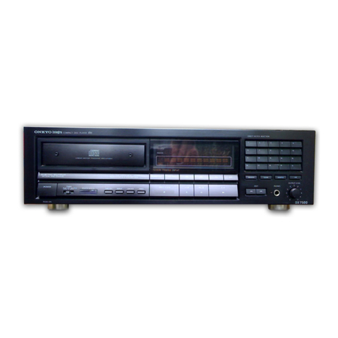
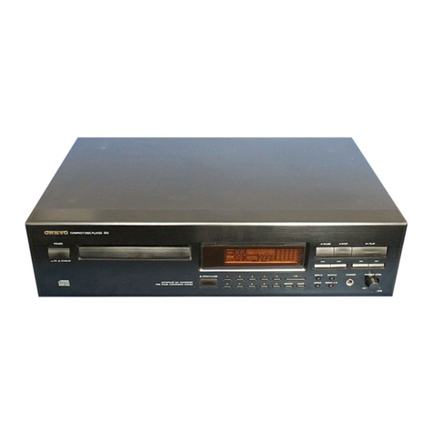
  9. Onkyo DX-C120 User manual

Onkyo DX-C120 User manual

Other manuals for DX-C120

1

This manual suits for next models

2

Other Onkyo CD Player manuals

Onkyo DX-C370 User manual

Onkyo

Onkyo DX-C370 User manual

Onkyo C-707CHX User manual

Onkyo

Onkyo C-707CHX User manual

Onkyo C-711 User manual

Onkyo

Onkyo C-711 User manual

Onkyo DX-C206 User manual

Onkyo

Onkyo DX-C206 User manual

Onkyo DX DX-7555 User manual

Onkyo

Onkyo DX DX-7555 User manual

Onkyo DX-V801 User manual

Onkyo

Onkyo DX-V801 User manual

Onkyo DX-708 User manual

Onkyo

Onkyo DX-708 User manual

Onkyo DX-7110 User manual

Onkyo

Onkyo DX-7110 User manual

Onkyo DV-SP503E User manual

Onkyo

Onkyo DV-SP503E User manual

Onkyo DX-705 User manual

Onkyo

Onkyo DX-705 User manual

Onkyo DV-CP706 User manual

Onkyo

Onkyo DV-CP706 User manual

Onkyo DX-C540 User manual

Onkyo

Onkyo DX-C540 User manual

Onkyo C-705TX User manual

Onkyo

Onkyo C-705TX User manual

Onkyo C-773 User manual

Onkyo

Onkyo C-773 User manual

Onkyo DV-CP802 User manual

Onkyo

Onkyo DV-CP802 User manual

Onkyo DX-C210 User manual

Onkyo

Onkyo DX-C210 User manual

Onkyo DX-C310 User manual

Onkyo

Onkyo DX-C310 User manual

Onkyo DX-788F User manual

Onkyo

Onkyo DX-788F User manual

Onkyo DX-704 User manual

Onkyo

Onkyo DX-704 User manual

Onkyo C-755 User manual

Onkyo

Onkyo C-755 User manual

Onkyo DX-C530 User manual

Onkyo

Onkyo DX-C530 User manual

Onkyo DX-M505 User manual

Onkyo

Onkyo DX-M505 User manual

Onkyo DV-CP706 User manual

Onkyo

Onkyo DV-CP706 User manual

Onkyo C-7030 User manual

Onkyo

Onkyo C-7030 User manual

Popular CD Player manuals by other brands

Arcam CD23 Handbook

Arcam

Arcam CD23 Handbook

Sanyo MCD-Z1F Service manual

Sanyo

Sanyo MCD-Z1F Service manual

JVC RC-ST3SL instructions

JVC

JVC RC-ST3SL instructions

Technics SL-P9066 operating instructions

Technics

Technics SL-P9066 operating instructions

Marantz HD-CD1 quick start guide

Marantz

Marantz HD-CD1 quick start guide

Sony DVP-FX850 Service manual

Sony

Sony DVP-FX850 Service manual

Philips AZ1140 Instrukcja obs?ugi

Philips

Philips AZ1140 Instrukcja obs?ugi

Alpine 7909 owner's manual

Alpine

Alpine 7909 owner's manual

JVC CH-X350 instructions

JVC

JVC CH-X350 instructions

RCA RP-7923 instruction manual

RCA

RCA RP-7923 instruction manual

Pioneer DEH-P3550MP XM Operation manual

Pioneer

Pioneer DEH-P3550MP XM Operation manual

Philips Shockproof AX2102 brochure

Philips

Philips Shockproof AX2102 brochure

Philips CD582 user manual

Philips

Philips CD582 user manual

Philips AZ 6821 operating manual

Philips

Philips AZ 6821 operating manual

Lasonic MSU-2020 user manual

Lasonic

Lasonic MSU-2020 user manual

Denon DCD-1420 Service manual

Denon

Denon DCD-1420 Service manual

Panasonic SJ-MR100 operating instructions

Panasonic

Panasonic SJ-MR100 operating instructions

Cambridge Audio SONATA CD30 manual 

Cambridge Audio

Cambridge Audio SONATA CD30 manual 

manuals.online logo
manuals.online logoBrands
  • About & Mission
  • Contact us
  • Privacy Policy
  • Terms and Conditions

Copyright 2025 Manuals.Online. All Rights Reserved.

b)
On
40748)
Cevy.0y
ad)
COxcy40)
ONKYO
SERVICE
MANUAL
©“
COMPACT
DISC
PLAYER
MODEL
DX-C120
MODEL
DX-C220
MODEL
DX-C320
BMD,
BMDN
|120V
AC,
60Hz
MP
230V
AC,
50Hz
only
DX-C220
|
120/220V
AC,
50/60Hz
SAFETY-RELATED
COMPONENT
WARNING!!
S
Pp
EC
|
F
|
C
AT
|
O
N
S
COMPONENTS
IDENTIFIED
BY
MARK
A
ON
Compact
Disc
Automatic
Changer
Model
DX-C320/C220/C120
THE
SCHEMATIC
DIAGRAM
AND
IN
THE
PARTS
Signal
readout
system:
Optical
non-contact
LIST
ARE
CRITICAL
FOR
RISK
OF
FIRE
AND
Reading
rotation:
About
500
-
200
r.p.m.
ELECTRIC
SHOCK.
REPLACE
THESE
COM-
| |
(constant
linear
velocity)
PONENTS
WITH
ONKYO
PARTS
WHOSE
PART
Error
correction
system:
Cross
interleave
Reed-Solomon
code
NUMBERS
APPEAR
AS
SHOWN
IN
THIS
MANUAL.
D/A
converter:
1
bit
PWM/ACCUPULSE
MAKE
LEAKAGE-CURRENT
OR
RESISTANCE
Sampling
frequency:
352.8
kHz
(8
times
oversampling)
MEASUREMENTS
TO
DETERMINE
THAT
Number
of
channels:
2
(stereo)
EXPOSED
PARTS
ARE
ACCEPTABLY
IN-
Frequency
response:
=
2Hz
-
20kHz
SULATED
FROM
THE
SUPPLY
CIRCUIT
BEFORE
Total
harmonic
distortion:
0.004%
(at
1kHz)
RETURNING
THE
APPLIANCE
TO
THE
Dynamic
range:
=
6d
CUSTOMER.
Signal
to
noise
ratio:
96dB
Channel
separation:
90dB
(at
1kHz)
Wow
and
Flutter:
Below
threshold
of
measurability
Output
level:
2
volts
r.m.s.
Power
consumption:
13
watts
Power
supply
rating:
European
and
Australian
models:
AC
230V,
50Hz
USA
and
Canadian
models:
AC
120V,
60Hz
Worldwide
model:
AC
120V
and
220V
Dimensions
(W
x
Hx
D):
455
x
120
x
425
mm
(17-15/16"
x
4-3/4"
x
16-11/16")
Weight:
7.4
kg
(16.3
lbs)
ONKYO.
AUDIO
COMPONENTS
Specifications
and
external
appearance
are
subject
to
change
1
without
notice
because
of
product
improvements.
b)
Son
-107/
0)
Cevy10710)
COxyle)
TABLE
OF
CONTENTS
Specifications
........c
cece
cece cece
cece
eeeeeeseeeeeneeneeeans
Service
procedures
........ccccccccccceeeccueceseeeeeeeeeeeees
Caution
on
replacement
of
optical
pickup..............
Protection
of
eyes
from
laser
beam.....................
Laser
warning
labels
................ccccccec
ce
nse
ee
eeueeeees
IC
block
diagrams
and
descriptions
.....................
Packing
VIEW.........
ccc
ccc
ecnceseeeceeecececcecceuereeneeeneues
Pick-up
drive
unit
......c..
ccc
cece
ccc
ceecsseeeeseesenneees
Chassis-exploded
View...........cccccsccceeeeccecceuueeeeuves
Parts
List...
ccc
ccc
cceceenceseeseeevsseeessseceunuerecnees
Block
diagram............cccc
ccc
c
ccc
seecacueevccceeseesuseeeees
Adjustment
procedures
.........cccccccsesececsseuvacecvseess
Printed
circuit
board
view
from
bottom
side.........
Printed
circuit
board-parts
list............cccccseeeeee
eee
Control
position
and
names
..........cccccece
eee
eeneee
ences
SERVICE
PROCEDURES
]
1.
Safety-check
out
2
After
correcting
the
original
service
problem,perform
2
the
following
safety
check
before
releasing
the
set
3
to
the
customer:
3
Connect
the
insulating-resistance
tester
between
the
4
plug
of
power
supply
cord
and
chassis.
9
Specifications:More
than
10Mohm
at
500V.
.
Voltage
Selector
(Back
panel)
Worldwide
models
are
equipped
with
a
voltage
selector
to
conform
with
local
power
supplies.Be
sure
to
set
this
switch
to
match
the
voltage
of
the
power
supply
in
user's
area
before
turning
the
power
switch
on.
Voltage
is
changed
by
sliding
the
groove
in
the
switch
with
a
screw
driver
to
the
right
or
left.
Confirm
that
the
switch
has
been
moved
all
the
way
to
the
right
or
left
before
turning
the
power
switch
on.
220V
~
120V
~
at
AC220V
220V
~~
120V
~
at
AC120V
CAUTION
ON
REPLACEMENT
OF
OPTICAL
PICK
UP
The
laser
diode
in
the
optical
pickup
block
is
so
sensitive
to
static
electricity
surge
current
and
etc,
that
the
components
are
liable
to
be
broken
down
or
its
reliability
remarkably
deteriorated.
PRECAUTIONS
1.Ground
for
the
work-desk.
Place
a
conductive
sheet
such
as
a
sheet
of
copper
(with
inpedance
lower
than
10M2Q)
on
the
work-
desk
and
place
the
set
on
the
conductive
sheet
so
that
the
chassis.
2.Grounding
for
the
test
equipment
and
tools.
Test
equipments
and
toolings
should
be
grounded
in
order
that
their
ground
level
is
the
same
the
ground
of
the
power
source.
During
repair,carefulley
take
the
following
precautions.
(The
following
precautions
are
included
in
the
service
parts.)
3.Grounding
for
the
human
body.
Be
sure
to
put
on
a
wnist-strap
for
grounding
whose
other
end
is
grounded.
Be
particularly
careful
when
the
workers
wear
synthetic
fiber
clothes,
or
air
is
dry.
4.Select
a
soldering
iron
that
permits
no
leakage
and
have
the
tip
of
the
iron
well-grounded.
5.Do
not
check
the
laser
diode
terminals
with
the
.
probe
of
a
circuit
tester
or
oscilloscope.
b)
Con
b-10740)
Cl
evyi07
40)
Cex
ye)
PROTECTION
OF
EYES
FROM
LASER
BEAM
DURING
SERVICING
This
set
employs
a
laser.
Therefore,
be
sure
to
follow
Laser
Diode
Properties
carefully
the
instructions
below
when
servicing.
@
Material:
GaAlAs
@
Wavelength:
760~800nm
WARNING?!
@
Emission
Duration:
continuous
WHEN
SERVICING,
DO
NOT
APPROACH
THE
LASER
@
Laser
output:
max.
0.5mW*
EXIT
WITH
THE
EYE
TOO
CLOSELY.
IN
CASE
IT
[IS
NECESSARY
TO
CONFIRM
LASER
BEAM
EMMISION,
BE
SURE
TO
OBSERVE
FROM
A
DISTANCE
OF
MORE
THAN
30cm
FROM
THE
SURFACE
OF
THE
OBJECTIVE
LENS
ON
THE
OPTICAL
PICK-UP
BLOCK.
LASER
WARNING
LABEL
These
labels
are
located
on
the
mechanism.
*This
output
is
the
value
measured
at
a
distance
about
1.8mm
from
the
objective
lens
surface
on
the
Optical
Pick-up
Block.
DANG
ER
-
—INVISIBLE
LASER
RADIATION
WHEN
OPEN
AND
INTERLOCK
FAILED
OR
DEFEATED.
AVOID
DIRECT
EXPOSURE
TO
BEAM.
HAZARDOUS
LASER
AND
VARNING
OSYNLIG
LASERSTRALNING
NAR
DENNA
DEL
AR
OPPNAD
OCH
SPARREN
AR
URKOPPLAD.
BETRAKTA
EJ
STRALEN.
UTION
—
LECTROMAGNETIC
RADIATION
WHEN
OPEN
AND
INTERLOCK
DEFEATED.
ATTENTION
—ravonnement
Laser
ET
ELECTROMAGNE
IQUE
DANGEREUX
S
VARO!
OUVERT
AVEC
L’ECLENCHEMENT
DE
SECURITE
ANNULE,
AVATTAESSA
JA
SUOQJALUKITUS
OHITETTAESSA
OLET
ALTTIINA
NAKYMATTOMALLE
LASERSATEILYLLE.
ALA
KATSO
SATEESEEN.
ADVARSEL
USYNLIG
LASERSTRALING
NAR
DEKSEL
o $
0G
°
BRYTES.
UNNGA
EKSPONERING
FOR
STRALEN.
SN
2983615
81Y
“CLASS
1
LASER
PRODUCT”
Db)
Ou
10748)
Cl
Or
y207
40)
COR
Y10
IC
BLOCK
DIAGRAMS
AND
DESCRIPTIONS
CXD2500AQ
(Digital
Signal
Processor)
Weems
C4M
87)
CLOCK
creme]
cent
aaron
O—
vco!l
(9)
DIGITAL
PLL
vcoo(s)
ARI-PITCH
PCO
@d
DOUBLE
SPEED)
;
FIL
a
E
:
18-TIMES
:
OVERSAMPLING
SHAPER
FILTER
bp
On
P4087
48)
€
O71071
9)
CO
y4e
|
a
pOK
_{
1
|FousOkinpt
————“—*s—“C*s*—S~s~s—s—ssCs
Ta
OS
~—s|
OO
[DAOR
~—sIGFSoupue
Cid
2
_|Fsw___|_©
{Oust
filter
changeover
output
for
spindle
motor
||
43
[pao7
|
O
|DAO7
_—sJRFCK
ouput
|
_3
|MON
_|
0
[Spindle
motor
conmoloupu
|
|
44
(DAG
|O|DA06
—_—*(C2P0oup—
[4
[MpP___|
©
|Spindle
motorservoconmol
=
|
45
=IDAOS
~~]
O
JDAOS
~—IXRAOFouput
|
5
[mps
__|
0
[Spindle
motorservoconrol
==
ss
dT
|
46
DAS
~~]
O
DADA
~—[MNTSouput
|
6
{Lock
|
O
|HwhenGPSisthehighlevel
|
ss
|
_47_|DAO3.—
|
O
JDAO3_—s[MNT2oupur
Tz
ince
Oo]
ft
as
faz
fc
face
[MNTioupu
3
[vcoo
__|
0
jOscillation
circuit
output
for
analog
EFM
PLL.
_|
{
49
[pao1
|
O
|DAO!
_|MNTOouput
|
9
]¥cor
|
1
[Osciaton
cet
input
for
anslog
EFM
PLL.
[50
[APTR
|
O
{Control
output
for
aperture
correction.
H
when
R
ch.
|
8.6436MHz
[51
_|APTL
__|
©
{Control
output
for
aperture
correction,
H
when
L
ch.
_
10
[Test
_{
I
|Test
terminal
|
52
|vss
|
—|Groundterminad
ss
eee
|
ae
|
12
{vss
|
—|[Groundwermind
=
—i—i‘CsCizr
33.8688MHz
input.
13-15
INC
|
|
54
|xtao
|
(Crystal
oscillation
circuit
output
of
16.9344MHz.
|
16
|VPCO
_|
O
[PLL
charge
pump
output
for
variable
pitch
|
prs
Crystal
selection
input
terminal.
L
when
16.9344MHz.
17
]VCKI
|
[tose
input
for
variable
pitch
from
VCO
H
when
33.8688MHz.
av
16.934MHz
|
56
_|FSTT__|_O
|2/3
divided
oupmofpins53and54.
|
18
[FILO
_|
O
JFiter
output
for
master
PLL.
|
s7_jc4M
_—s|
o
|4.2336MHzoupus—
|
49
[RII
——s|_._
{Fitter
input
for
master
PLL.
|
58
Ic16M
_|_O
116.9344
MHz
output
|
29
|pco
_|
©
[charge
pump
outputof
masterPLL
|
|
59
(MD2_—_s_T_{
Digital
output
control
input.
On
at
high
level.
22
|cttv
[1
|VCOconmol
voltage
inputfor
master
=|
|_61_|EMPH
|
_O
|Emphasis
control
output.
Active
high.
[23
JAVDD
|
__
[Analog
section
power
supply
(+5V)_
=|
|_62_|WFCK
__|
O
Write
frame
clock
output
|
24
|RF
|
1
|EFMsignalinpot
|
&
fscor
0
Sub-code
detection
output.
H
when
is
detected
SO
|
25
(BIAS
_|
1
|Asymmesy
circuit
constant
current
input
or
SI.
26
fasy1
|
1
[Asymmetry
comparator
voltage
input
______——«di
|
64
|SBSO
_|
©
|Serialouputofsub-codeP~W)
[28
jasye
[1
|Asymmewyconuolcircut,
|
fsaso
|
0
Sub
Q
80
bits,
PCM
peak,
and
level
data
16
bits
|
29
inc.
SEO]
|
——C—C“‘CSC‘C
output.
OO
PSSL
o
Audio
data
output
mode
changeover
input
|
67
{sock
{1
Clock
input
for
read
out
SQSO
Serial
data
at
L
and
paralier
data
at
H.
|
68
[MUTE
|
©
|Mutingcontroloutput.ActiveH.
31
[wock
[|
1
[D/A
interface
for
48
bits
slot.
Word
clock
f=2Fs.
_
|
|
69
|SENS
|
_[Sens
output.
Output
to
the
microprocessor
|
32
|LRCK
|
1
[D/A
imerface
for
48
bits
slot.
LR
clock
f=Fs.
|
|__70_[XRST
_|
I
|Systemreset.Resetatthelowlevel.
|
33
|[vpp
__|
_[Powersupplyterminal(+5V)
|
|
71
(DATA
_|_I_
|
Serial
data
input
from
the
microprocessor.
13449)
8
8=6pT
Data
output
terminals
XLTA
a
Latch
input
from
the
microprocessor.
re
eS
Latch
the
serial
data
at
the
trailing.
|
34
|pais
_|
oO
|DAI16
_|Seriatdata
of 48
bits
slot_
|
73
|vpp
_|_
_|Powersupplyweminl
|
35
|pais
|
O
[DAIS
_[Bitclockof
48
bits
slot__—_|
|
74
|[ctoK
_|
1
[Serial
data
transfer
clock input
from
microprocessor
_
|
36
|DAI4
_
|
O
|DA14
_|Serial
dataof
64
bits
slot__|
|
75
|SEIN
__|
I
|Sens
input
from
SSP
|
37
|DAI3__
|
O
|DAI3_
_|Bitclock
of
68
bits
slot
—_—
|
76
_|CNCI___|_I_|
Track
jump
numbers
count
signal
input
|
38
|pai2
|
©
[DAI2
—_—_—|LRclockof
68
bitsslor__—is
'_77_|DATO
_|
©
|SerialdataouputtoSSP_
Cid
|
39
[pau
|
o|pau
_—|GroPoupr
|
78
|x~To
|
|
40
{patio
_|
O}DAIO
_—{xuGFoupu
Cs
|
79
|CLKO
Note:
SSP:
1C101
CXA1372Q
BA6191
(Motor
Drive)
y)
ED)
9
Wy)
™
D<
££
TD
DD
€&
GO
OQEg«é
+
Er
FF
Ff
F
:
Forward
A:
Backward
bp
Gl
On
40748)
Covyey
48)
CO
ys6)
CXA1372Q
(Servo
Signal
Processor)
(»)
19401
Gs)
21
@r)224
(in)
aan0
nose
YOIVYVANOD
MOONIM
46
(6)
S19
HWO0IW
Lhd
LN
w21S5/530
vivo
WwW
4300330
$S34H00¥
#3151934
4d1H5
LNGN)
NOLLYSNIDMOD
36
VHd
ONINOVAL
d01ss(a1)
The
sled
runaway
prevention
circuit
operates
at
the
low
level
Serial
data
transfer
clock
input
from
microprocessor.
Q
is
DESCIRPION
IPINNO.
SYMBOL
[VO
|DESCIRPION,
et
CisCsCisS
IVC
tT
|
Mid-point
voltage
input
terminal.
|
__23|XLT_
tT
[Latch
input
terminal
for
microprocessor.
|
a
Connect
the
capacitor
between
FS3
andthispin
{|
24IDATA___|_
I
[Serial
data
input
terminal
for
microprocessor.
2)FGD
when
the
high
frequency
gain
focus
servo
|
2SIXRST_
{I
[Resetinputterminal.Activelow.
is
dropped.
|
26/C.OUT
|
O
[Signal
outputto
count
the
track
numbers.
3/FS3
Focus
servo
high
frequency
gain
changeover
|
2TSENS
|
9]
This
terminal
outputs
FZC,and
SSTOP
to
a
scoring
command
fom
te
microprocessor
FLB
Input
terminal
for
the
low
frequency
boost
of
|S
29|MIRR___|
O
|Mirrorcomparator
output
terminal,
pe
Tectus
servo
aueney
Boost
of
|_§
Oe
SS
FEO
___|
O
|Focus
drive
outputterminal,
|S
STASY
|
T._
[Auto
asymmetry
control
input
terminal.
|
«SFE-
|
I
|Inversion
input
terminal
of
focus
amplifier.
|
~——Ss32]EFM__—_—«|
O
[EFMccomparatoroutputterminal.
|
SRCH
YT
Time
constant
terminal
to
make
the
focus
search
[
33/FOK_—s{
O
[FocusOK
comparator
outputterminal.
_—=s_—_i|
waveform.
|
34ICCr
tO
[Defect
bottom
hold
outputterminal.
PRU
TT
Tracking
high
frequency
changeover
input
|
35}CC2_
|
[Defect
bottom
hold
input
terminal
from
CCl.
_—|
terminal.
|
37/CB_
s|_T
|Defect
bottom
hold
capacitor
connection
terminal.
|
|___1i|TAO
|
0
[Tracking
drive
outputterminal.
SSS
(CP
=|
[Mirror
hold
capacitor
connection
terminal.
_—_—|
|
2ITA-
iT
[Inversion
input
terminal
of
tracking
amplifier,
|
SOIRFI_
|
I
(RF
summing
amplifier
inputterminal.
ss
|__13{SL+
|
T_[No-inversion
input
terminal
of
sled
amplifier.
|
40|RFO
_|
O
[RF
summing
amplifier
output
terminal.
=i
|__14|SLO_|
©
[Sled
drive
outputterminal.
ss
SSS~=*«idC*S*C*C*~‘STZC~S~SC*”=ST-
|
Tracking
zero-cross
comparator
input
terminal.
_|
|___IS|SL-___
fT
[inversion
input
terminal
of
sled
amplifier.
|
—43(TE
_—'|
1
|Trackingerrorinputterminal.
a
focus
tracking.
when
defect.
a
ee
17|/ISET
focus
search,tarcking
jump,and
sled
kick
height
detection.
is
decided.
|
46/FZC_
|
[Focos
zero-cross
comparator
input
terminal.
|
|
__I8|/SSTOP___|
1
[Inner
switch
selection
inputterminal.
|
_47(FE
__|_I
[Focus
error
input
terminal.
PTs
einai
used
when
wack
jump.
—__
{48
FDFCT
a
Capacitor
connection
terminal
for
time
constant
21)/LOCK
SF
ion
circui
when
defect.
Se
bp
On
40740)
Oyr-107
48)
COKy10
SM5872CN
(D/A
Converter)
MCOM
LRCI
BCKI
DI
O——@——@—@
pt
MDT/FSEL1
MICROPROCESSOR
NTERF
C
INTERFACE
pie
nies
(5)
MUTEO
MCK/FSEL2
(12)
&
INFINITY/ZERO
Co
DE-EMPHASIS
DETECTOR
MLEN/DEEM
SELECTOR
MUTEI
ATTENATION
(6)
COUNTER
FILETR
PROCESSING
&
ATTENATION
PROCESSING
NOISE
SHARPER
&
PROCESSING
PWM
DATA
GENERATION
BLOCK
AVDDi
(17)
LO
AVSS1
LON
AVDD2
AVDD3
RON
AVSS2
RO
|
1
|xXTO
|
©
[Resonatorsection
28
(TH
|
[Resonatorsection
|
2
|xvss
|
|Ground
for
resonator
system
|
27
|XVDD
|
[SV
forresonatorsysiem
p33
ick
trp
6
avd
|
[SV
foranalog
section
icKo.—s«L-O|
Output
clock
of
resonator
section:
384fs
|
25
|IRo
if
ol
R
ch
PWM
output
(+)
|
5
|[MUTEO
|
0
[Infinity
zero
detector
output
|
24
[AVSS2__|
[Ground
for
analog
section
|
6
(MUTED
|
1
[Mutingourpu
|
23
(RON
|
OR
ch
PWM
output
(~)
|_7
|Mcom
[J
[Interface
switching
control
|
22
|avpp3
|
_
[SV
foranalogsection
|
8
|tRcr
|
1
|Sampling
rate
clock
of
input
data:
H=Lch,L=Rch_
|
21
|avpp2
|
[sv
foranalog
section
BCKI
|
1
[Bitclockofinpurdata
|
20
[LON
0
Ich
PWM
output
(+
ch
PWM
output(+)
|
10
[pr
|inpurdata
ss
—<—s—SCSCCCSS
ASST
|
—_[Ground
for
analog
section
SELL
fam
egieneyse
ais
|i
0
——_1
0
pout
|
__
|
12
|FSEL2
_|_I
|When
FSEL1,FSEL2,
and
MCOML
are
the
low
level.|
17
|AVDDI
|
[5Vforanalogsection
sss
|
13
|DEEM__|
I
|De-emphasis
contol
input
S|
16
IDVDD
|
—s[SWfordigital
section
=|
[|
14
|RSTN
|
|Systemreset:
L=Reset
—s—i‘C!S*dL«sS
=[DVSS
|
~—[Ground
fordigital
section
|
DX-C120/DX-C220/DX-C320
as—nd
gulyren
ie
uoneiedg
:
+
asind
suipes]
1
uoneiedg
:
|
indut
191J9Au09
C/V
:
OL'6'8'L'9
[9Q3|
MOT
9171
18
UOTIRIOdG
:
FT
[99]
YStY
Oy
1
UONIeISdO
:
H
Po
NT
08
posm
ON}
Pt
NT
Po
NT
8
ar
2
ae
ar
rr
er
a
Oqn]
JOWSIPUT
1Us9ss10NT
JOJ
indjno
1wawses
3qm
“Jj JO]
0
oN
ai
aqni
JOWDIpPUT
1UasSaIONy
10y
indino
1awgas
|
LC
8d
posn
1on[—_[
[ONT
ee
TS
<I
JWNT=J
WSWIOp=H)
YARIIq
[ssNosed
3y1
SUTNIDS
a
ANVAAALLAINOU
IOIOUS
SUIPBOT
JOJ
JUDLINDIOAO
JO
PeUDIS
9ATIDIOC]
pT
YT
|
INAYHOO
AT
INGUT
YONAMS
SUIQSIUIy
Usdo
SUIyYSNY
oT
TRO]
T
7 7
7
H
110d
JNGul
[EUSIS
JONUOS
S1OWIy
|
BIS
SUIZIUOIMIUAS
i
at
UU
PN
es
ee
re
<i
ON
PA
ct
iT
| J |
—
fy
TT
|
|
O
|
ON)
\S)
Zz.
ee)
MS'SASOTO'
AT
Zz
EE
.
el
AU
a6
v,
aa
O
Alo
Sl
asl
&
6S 8S
to
wy
9¢
gs
vs
t
=f
ON
Wp
wy
Wy
0s
cn
3
t~}
06
Jeusis
jONUOS
Surjony5
|
T
[0
ASO
IOHS
|
1
|
0)
TLOW
T
|
0
avLowd
iy
[@Snore-)
HO]
|
OF
|
JNGUT
IGNUSIUt
OJOYC
JOIDS1ap
UOTISOd
ISIp
[BsNnoIw;
a
.
°
BE
INCU!
JNIANLIIIUI
OJOY
UONOdep
UOTITSOd
dos
[asnore7)
PH]
TE
|
SNaS
dOLS
LOW
ce
[BUSTS
[ONUOS
1ase
]
PH
|
0
|
|
9
INdiNG
UONE[[I9SO
yO[O
WaIsAS
ff
8]
|
SE
NUE
UOTE]{IOSO
YOO
WIDISAS
P|
PE
ee
ca
pesTIONT
JN]
Ct
[EUILLID]
UOTISIj9S
[OPO]]
||
D919§
TIED-KA
Te
|
SO[CUY
10}
EUILLIOT
ATUANS
osel[OA
SdUaIOsOy
ni
|
OF
ka
87
Le
rr
ia
JBusIs
JONUOD
UOTIEIOI
[asnores)
mr
=
rs)
~
Z
#4
.
wv
a
‘DS
|
&
~
es)
al
al
S|
>
gi
ol
el
BIS
<|
<|
<|
=
S|
xe]
S13
gl
OI
SUISSID0Jd
[BUSIS
WOOL]
[RUSIS
ISUag
ee
RON
ONT
ST
J
SUISSODOId
[BUSTS
07
CG)
APOd
Qns
JO
YDOID
JOJSURN
[BLISS
Pe
[O]
AOOS|
FF
jeudts
SUNN]
H
LAW!
€1
__
een
HO
|
ca
<p
dutssoooid
jeudis
01
jeusdis
Surin
PH
|
0)
INWd
PoE
TESCO
TOT
ERT
>i
suIssaooid
[eUsIS
JO
PUbLULIOD
JO
BIep
[ellos
HO
|
VLIVd
|
OT
“DI
1088390010
[BUSIS
SY]
OF
PUBUIIOS
JO
[RUTULIAT
NANO
YOO[O
Josue
[BLS
|
{Of
HY
6
|
Assy
eT
rams]
YT
[ea
|
DOU
L
94
SQN]
LOIWIIPut
JUsoSaIONI
JOJ
speutuai
indino
1W3ig)]
H
El
¢
OS]
€
pas
109
RT
posmionf
of
fT
CY
vonduoseq]
=
[ON]
=
1OQwAS|
ON
(sossed0idoi0IN)
Z8O0-4DEvO8Ldd”
ll
EECEG
PACKING
VIEW
PARTS
LIST
REF.NO.
PART
NO.
201
82115018
202
27270357
206
29052854Y
29058255
Y
29052856Y
207
8
29091658Y
208
29091
659Y
209.
=
29100141Y
210
29110071
21)
282301
214
=
29095721Y
246
29360840Y
217
=
29355207Y
218
29360687Y
219
29361791Y
29361792Y
29361793
Y
29360708
Y
b)
en
40743)
Cl
Ory07
48)
COCy16)
DESCRIPTION
5P+18FN,
Screw
t0.5x
15x
5.2,
Spacer
Master
carton
box
<DX-C120>
Master
carton
box
<DX-C220>
Master
carton
box
<DX-C320>
Pad,
L
Pad,
R
700
x
600,
Poly
bag
Damplon
tape
Sealing
hook
Sheet,
Door
Label,
sheet
Instruction
sheet
Label,
Class1
<P>
Label
(UPC),
<N>,
DX-C120
Label
(UPC),
<N>,
DX-C220
Label
(UPC),
<N>,
DX-C320
Label
(UL),
<N>
PART
NO.
DESCRIPTION
Accessary
bag
ass'y
2010098A
Connection
cord
2010200
Remote
control
cord
24140289Y
RC-289C,
Remote
control
unit,
Except
DX-C110
3010054
UM-3,
Two
batteries,
Except
DX-C120
29342095
Y
Instruction
manual,
E
29342096Y
Instruction
manual,
<V>
29342097Y
Instruction
manual,
6
Land
<P>
29342098
Y
Instruction
manual,
3
Land
<W>
29365019AY
Warranty
card
<N>
29365020L,
Warranty
card
<V>
29358002K
Y
Service
station
list
<N>
25055040
CV-K-2,
Converstion
plug
<W>,
DX-C220
Only
29100097-1
350
x
250,Styrene
bag
29100094B
Styrene
bag
for
warranty
card
<V>
<D>:
120V
model
only
<P>:
230V
model
only
<W>:
Worldwide
model
only
<N>:
U.S.A.
model
only
<V>:
Germany
model
only
<C>:
Canadian
model
only
=)
N
o
9
~<
(a)
“~
©
“I
N
Oo
~<
Co
~
©
N
™
2
o<
a
MECHANISM-EXPLODED
VIEW
—~10—