Oval EL7510 User manual

1
Every OVAL product is fabricated, tested, and inspected under stringent quality control before it leaves our
factory.
To derive maximum benet from the product, we recommend you to be well familiar with the information and
instructions given in this manual before you place it in service and retain this manual at the eld location for
ready reference.
DATA COMMUNICATOR
Ins. No. E-922-1-E
MODEL : EL7510

E-922-1-E
2
CONVENTIONS
Shown in this manual are the signal words NOTE, CAUTION and WARNING, as described in the
examples below:
NOTE: Notes are separated from the general text to bring the user's attention to
important information.
CAUTION: Caution statements signal the user about hazards or unsafe practices
which could result in minor personal injury or product or property damage.
WARNING: Warning statements signal the user about hazards or unsafe practices
which could result in severe personal injury or death.
1. PREFACE............................................... 3
2. SAFETY PRECAUTIONS ...................... 3
2.1 Conrming the Nameplate .............................. 3
2.2 Structural Notice ............................................. 4
2.3 Explosionproof Precautions ............................ 4
3. GENERAL INFORMATION.................... 5
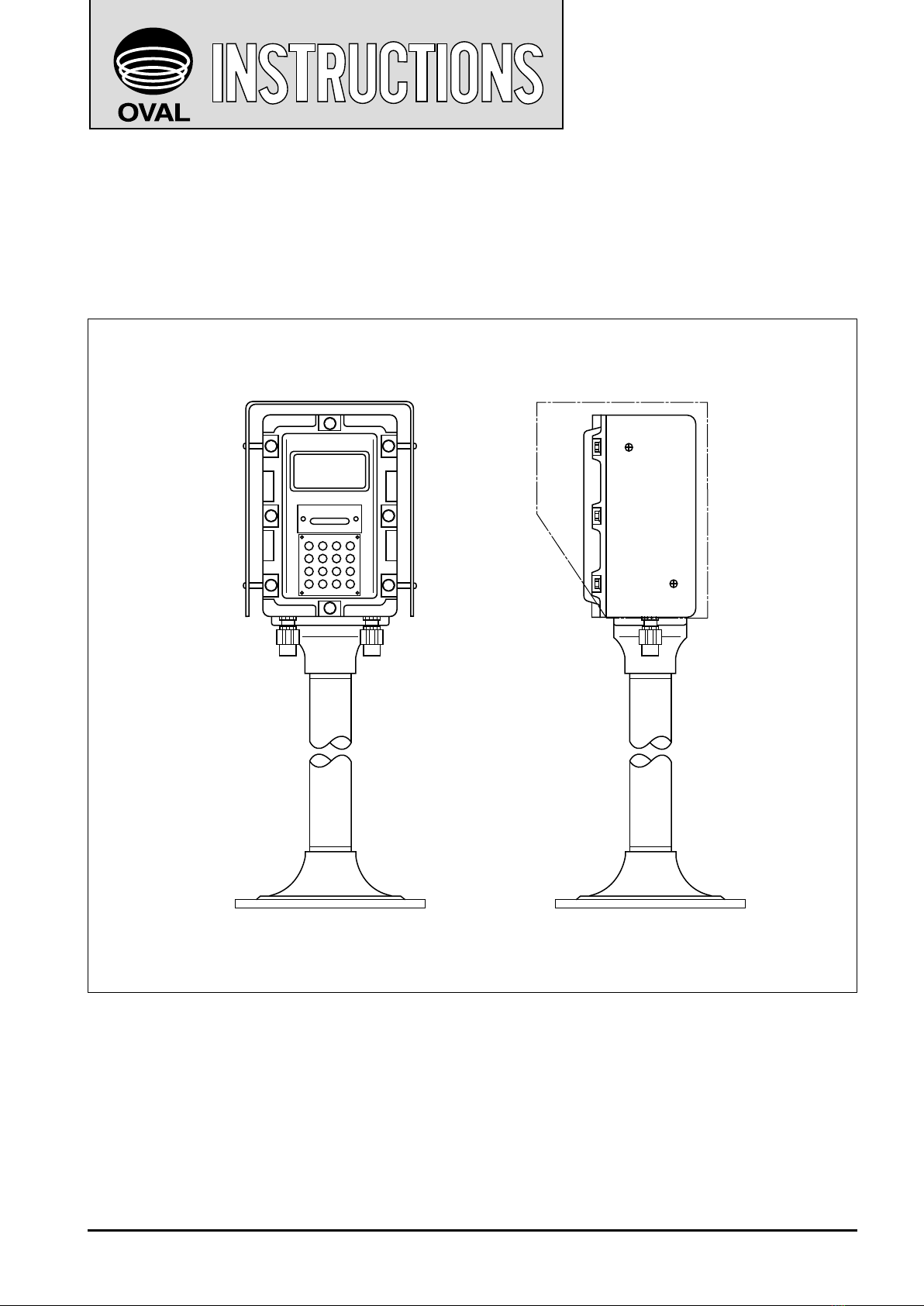
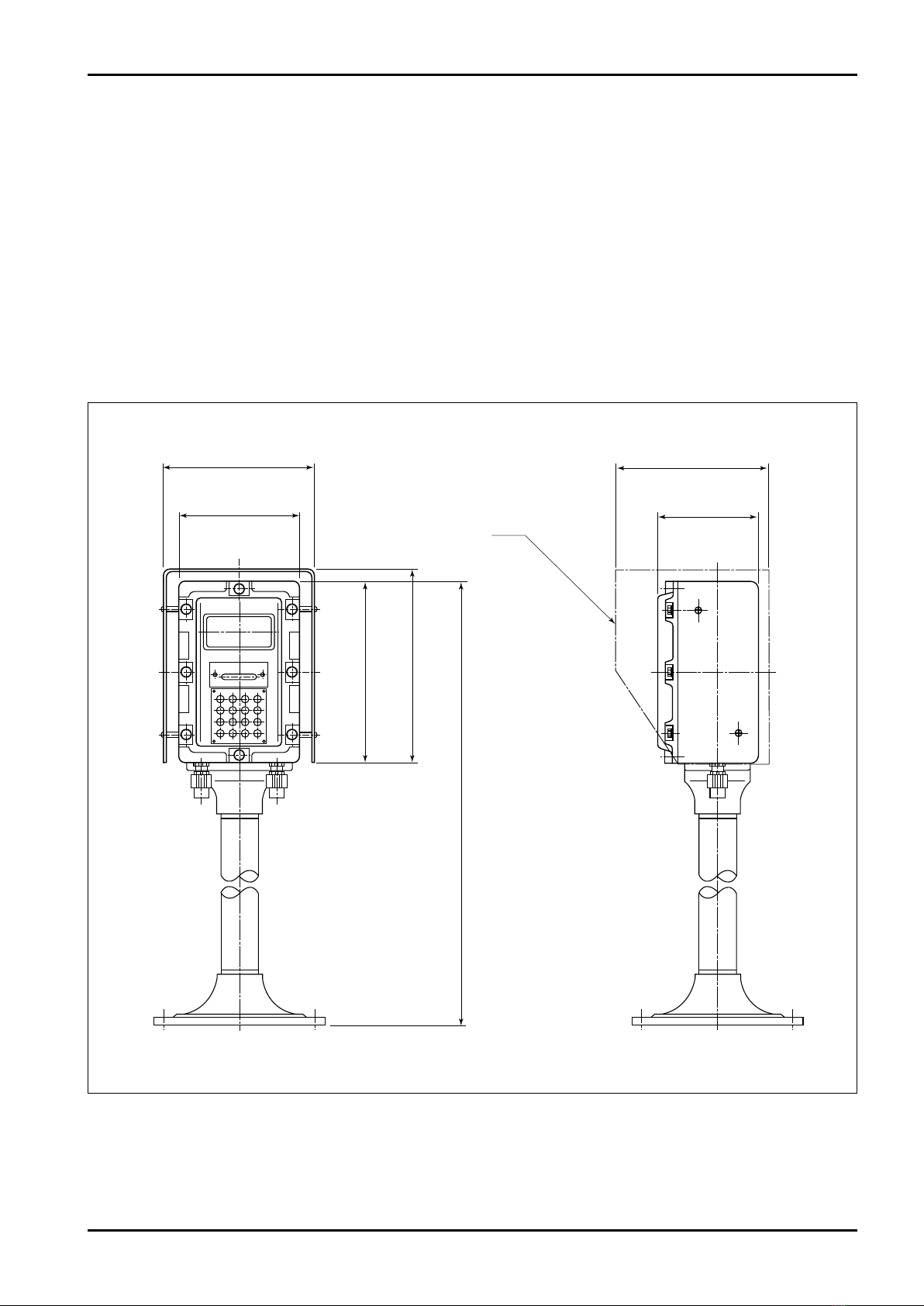
3.1 Features........................................................... 5
3.2 Appearance .................................................... 5
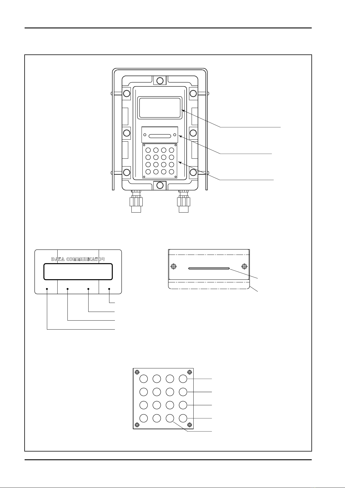
3.3 Part Names...................................................... 6
3.4 Instrument Internal Conguration
Block Diagram................................................. 7
4. INSTALLATION...................................... 8
4.1 Installation ....................................................... 8
4.2 Wiring .............................................................. 8
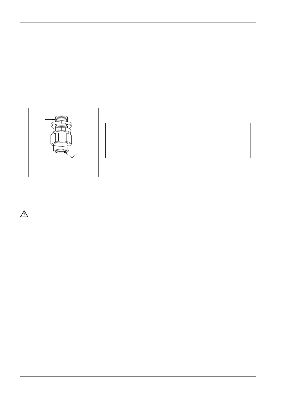
4.2.1 Wiring Cables .....................................................8
4.2.2 Connecting Method............................................9
4.2.3 External Terminal Connections.........................10
5. FUNCTIONAL SETTINGS ................... 11
5.1 Functional Settings........................................ 11
5.2 Hard Switch................................................... 11
5.3 Soft Switch .................................................... 12
6. OPERATION ........................................ 13
6.1 Outline Flow .................................................. 13
6.2 Card Input Processing................................... 14
6.3 Key Input Processing
(with numeric keypad function) ..................... 17
6.4 Display Processing........................................ 19
6.5 Other Processing........................................... 22
7. COMMUNICATION RETRY
FUNCTION........................................... 23
8. MAGNETIC CARD READING
SYSTEM............................................... 24
8.1 Magnetic Card Recording Format................. 24
8.2 Card Data Read............................................. 24
9. NON-CONTACT IC CARD READING
SYSTEM............................................... 25
9.1 Non-contact IC Card Recording Format ....... 25
9.2 Reading Non-contact IC Card....................... 26
10. TROUBLESHOOTING ....................... 26
10.1 Power Cannot be Turned On....................... 26
10.2 Card Cannot be Read
(Frequent occurrence of "Card read error")
... 26
10.3 Numeric Keypad Does Not Respond
(with numeric keypad function) ................... 28
10.4 No Communication with Host System ........ 28
11. STANDARD SPECIFICATIONS......... 29
11.1 General Specications ................................ 29
11.2 Communication Specications ................... 29
11.3 Display Specications ................................. 29
11.4 Card Reader Specication .......................... 30
11.5 Numeric Keypad Specications .................. 30
11.6 MIFARE Card Specications ....................... 30
12. Product Code Explanation............... 31
CONTENTS

E-922-1-E
3
1. PREFACE
The data communicator (hereinafter this instrument) has been thoroughly tested and inspected before shipment
from our factory.
When you receive this instrument, check the appearance for possible damage.
First of all, thoroughly read the handling precautions described in this section.
For topics other than those covered in this section, refer to the respective sections of this manual.
If you have something to inquire, contact the sales ofce from which you purchased the instrument, or the
nearest OVAL representative in our customer service network.
2. SAFETY PRECAUTIONS
2.1 Confirming the Nameplate
The nameplate (explosionproof caution label) placed at the lower part of the left side of this instrument
describes the specications of this instrument.
In reference to the standard specications (Section 11) and product code (Section 12), make sure to see that
the instrument you received conforms to the specications you ordered.
形式
電源
製造番号
シリアル番号
製造年月
製造者名称
形式の名称
防爆構造に
関する記号
定格
本安回路
非本安回路
周囲温度
注意事項
注意事項
株式会社オーバル
EL7511
EL7512
EL7513
Exd[ib]ⅡBT4
最大電圧 15.8V
最大電流 27.2mA
最大電力 91.1mW
電源 240VAC50/60Hz
消費電力 35VA
出力回路許容電圧
250VAC 50/60Hz、 250VDC
60℃
本安接地端子の接地は単独A種接地工事のこと
部品、配線等の変更または改造を行わないこと
耐熱温度 70℃以上のクーブルを使 用すること
電源遮断後、3分経過するまで蓋を開けないこと
設置、配線等の詳細は取扱説明書(No.E-922)
参照のこと
EL7511:カード読取り部
EL7512:カード読取り部+表示部
EL7513:カード読取り部+表示部+テンキー部
9 52 50 0 0 41
Product specifications Explosionproof specifications
労( )検
第C15359号
株式会社
オーバル
Industrial Safety and
Health Act Examination
Nameplate
E L 7 5 1 -
VA C 5 0 / 6 0 H z
Fig. 2.1

E-922-1-E
4
2.2 Structural Notice
(1) This instrument has explosionproof and waterproof conguration to be ready for outdoor applications.
When you remove the front cover for parameter setting, wiring or the like, be sure to avoid bite of wiring
cable when you restore the instrument.
(2) The pressure-resistant packing unit attached is a part of the pressure-resistant explosionproof construction.
Do not use any pressure-resistant packing other than attached. The union of the pressure-resistant packing
must be tightened sufciently after completion of wiring.
(3) The packing in the pressure-resistant packing unit shall be selected among three different packings (φ11
provided as standard, φ12, and φ13.5) in accordance with the outer diameter of the nished cable.
2.3 Explosionproof Precautions
CAUTION: The following items are the requirements for conforming to the
explosionproof test for this instrument. When you place this instrument
in service, be sure to keep the following precautions.
(1) The grounding for safety grounding terminal shall be single class A grounding.
(2) Do not change or modify the parts, wiring, etc.
(3) Use heat-resistant cables that withstand 70°C min.
(4) Do not open the front cover till 3 minutes passes after power off.
(5) Perform installation, wiring, etc. in accordance with the following conditions.
• The places where this instrument can be installed are risk class 1 and 2.
• In order to retain the explosionproof capability of this instrument, apply single class A grounding work to
the number 16 (ground) of the external wiring terminal block. (Shunt diode type burrier is built in this
instrument.)
Packing code Packing inner
diameter
Packing inner
diameter
11 11 10.0 to 11.0
12 12 11.1 to 12.0
13.5 13.5 12.1 to 13.5
Cable dimensions
Fig. 2.2 Pressure-resistant
packing unit
G 3/4
G 3/4
Unit: mm

E-922-1-E
5
3. GENERAL INFORMATION
3.1 Features
This instrument is an explosionproof type card reader conforming to non-contact IC card (MIFARE card
ISO14443 type A) or contact type magnetic card (JISX6301 model II).
Data entry is available in two ways, using a card reader or a numeric keypad. In addition, entry from the
communication port is displayed on the LCD.
Communication interface is via RS422 (RS485).
3.2 Appearance
(A Model with Display + Magnetic Card Reader + Numeric Keypad Specifications)
300
200
Cap
300
240
360
380
1500 (Standard)
Fig. 3.1

E-922-1-E
6
3.3 Part Names
7
4
1
0
8
5
2
.
9
6
3
F
f
CL
ENT
SEND
SEND key
ENTry key
CLear key
<Magnetic card reader slot, detail>
<Data entry numeric keypad, detail>
Card slot
Card slot cover
F input key
f input key
25. #/- %22 02/
Display or non-contact IC card
reader window
Magnetic card reader slot
Data entry numeric keypad
<Display and non-contact IC card reader window, detail>
Not used
ERROR lamp
COMMUNICATION lamp
CPU RUN lamp
25. #/- %22 02/
Display or non-contact IC card
reader window
Magnetic card reader slot
Data entry numeric keypad
<Display and non-contact IC card reader window, detail>
Not used
ERROR lamp
COMMUNICATION lamp
CPU RUN lamp
7
4
1
0
8
5
2
.
9
6
3
F
f
CL
ENT
SEND
SEND key
ENTry key
CLear key
<Magnetic card reader slot, detail>
<Data entry numeric keypad, detail>
Card slot
Card slot cover
F input key
f input key
Fig. 3.2

E-922-1-E
7
3.4 Instrument Internal Configuration Block Diagram
Constant
voltage unit
9
to
14
LED
×4
Power supply
85 to 240 VAC
16 characters
x 2 lines
Comm. port
Terminal block
Display
Numeric Keypad
UART
CPU
ROM
32k
RAM
16k
RAM
16k
Card control
Magnetic
stripe
Non-contact
IC card
0 through 9, ., CL,
ENT, etc.
LED and switch
input control
LCD control LCD
RS422
o r
RS485
Fig. 3.3

E-922-1-E
8
4. INSTALLATION
4.1 Installation
<Installation Location> Detail of location is subject to explosionproof guide 2000.
Although this instrument is all-weather type (with a cap for preventing direct sunlight), install this instrument in
a place where the display is not exposed to direct sunlight as much as possible.
CAUTION: Avoid the following places for installing this instrument.
• A place where corrosive gas may occur or a dusty place
• A place where vibration or shock is frequent or where vibration or
shock is always present
• A place where ambient temperature is below -20°C or above 60°C
• A place close to the power circuit or a place severely affected by
inductive interference
• A place the operator faces the sky while using the display or numeric
keypad
Otherwise, malfunction or failure may occur.
4.2 Wiring
4.2.1 Wiring Cables
<Wiring cables>
Detail is subject to explosionproof guide 2000.
(1) For communication cables, use twisted paired, electrostatically shielded, vinyl sheathed control cables (0.75
to 2.0mm2) or equivalent.
(2) For power line, use insulated vinyl sheathed control cables (CVV 0.75 to 2.0mm2) or equivalent.
(3) Using crimp-type terminals at the end of wiring, ensure good electrical connections.
<Wiring Connections>
Use the cable connector specied by OVAL.
WARNING: Before wiring the instrument, make sure that the power source is
disconnected.
Wiring with power on may result in electrical shock.
WARNING: • Avoid using a power supply with large voltage variation.
• Do not install the communication line close to or in parallel with the
power lines or high-voltage lines.
• Connect the end of shielded cable to ground.
• Connect the power lines and communication lines correctly.
Otherwise, the instrument may ruin.

E-922-1-E
9
4.2.2 Connecting Method
(1) RS422 half duplex system (1 to 1) (2) RS422 full duplex system (1 to 1)
(3) RS485 half duplex system (1 to 1) (4) RS485 full duplex system (1 to 1)
+
−
Terminating resistance 330 7
Opposite side
9 10 11 12 13 14
+ − SG + − SG
RXD TXD
Card reader
+
−TXD
+
−RXD
Opposite side
+
−
Opposite side
+
−TXD
+
−RXD
Terminating resistance 110 7
Opposite side
Terminating resistance 330 7
Terminating resistance 110 7
9 10 11 12 13 14
+ − SG + − SG
RXD TXD
Card reader
9 10 11 12 13 14
+ − SG + − SG
RXD TXD
Card reader
9 10 11 12 13 14
+ − SG + − SG
RXD TXD
Card reader
Fig. 4.1

E-922-1-E
10
(6)RS485fullduplexsystem(Multidrop)
TXD
RXD
Opposite
side
+
−
+
−
n = 16 max.
Terminating
resistance
110 7
9 10 11 12 13 14
+ − SG + − SG
RXD TXD
Card reader n
9 10 11 12 13 14
+ − SG + − SG
RXD TXD
Card reader 2
9 10 11 12 13 14
+ − SG + − SG
RXD TXD
Card reader 1
4.2.3 External Terminal Connections
1 2 3 4 5 6 7 8
9 10 11 12 13 14 15 16
H N G
+ − SG + − SG
POWER
RXD TXD
COMMUNICATION
(5)RS485halfduplexsystem(Multidrop)
+
−
n = 16 max.
Opposite
side
Terminating
resistance
110 7
9 10 11 12 13 14
+ − SG + − SG
RXD TXD
Card reader 1
9 10 11 12 13 14
+ − SG + − SG
RXD TXD
Card reader 2
9 10 11 12 13 14
+ − SG + − SG
RXD TXD
Card reader n
Fig. 4.2

E-922-1-E
11
5. FUNCTIONAL SETTINGS
Settings for the function of this instrument such as transmission rate, etc. are implemented by the hard
switches and soft switches. For the items of functional settings, refer to the Function Settings shown below.
5.1 Functional Settings
Function Settings Method for selection
Interface RS422 (RS485) —
Transmission rate 1200, 2400, 4800, 9600 (bps) Hard switch
(DSW-1)
Data bit length 7, 8 (bit) Soft switch
Delimiter setting CR, CR+LF Soft switch
Parity None, Odd parity, Even parity Soft switch
Stop bit 1, 2 (bit) Soft switch
Local address 0 to 16 (stations) Hard switch
(DSW-1)
Mode selection Active mode, Polling mode Soft switch
5.2 Hard Switch
The hard switch (hereinafter DSW-1) is located on the internal board. With DSW-1, you can set transmission
rate and local address.
DSW-1
LCD
Not used
Transmission
rate
0: 1200 bps
1: 2400 bps
2: 4800 bps
3: 9600 bps
Local address
0: Station 1
1: Station 2
F: Station 16
1
2
0
2
2
1
3
2
0
4
2
1
5
2
0
7
2
2
8
2
3
6
2
1
(SW number)
Internal board
• DSW-1 Setting
to
DSW-1
LCD
Not used
Transmission
rate
0: 1200 bps
1: 2400 bps
2: 4800 bps
3: 9600 bps
Local address
0: Station 1
1: Station 2
F: Station 16
1
2
0
2
2
1
3
2
0
4
2
1
5
2
0
7
2
2
8
2
3
6
2
1
(SW number)
Internal board
• DSW-1 Setting
to
CAUTION: Set DSW-1 appropriately to meet
your operating environment.
If you set it incorrectly,
malfunction or damage of
instrument may occur.
Fig. 5.2
Fig. 5.1

E-922-1-E
12
5.3 Soft Switch
Soft switch is a ROM memory table located on the internal board. The functions of the instrument are selected
by the data written on the ROM. Communication parameters and communication modes are categorized by
the function setting table in the ROM.
(1) Communication parameters
Data length, parity, and stop bit length for serial communication are specied.
Address: 00F2h
Range: 0 to 9 (Decimal)
Value Data length Parity Stop bit length
0 7 Odd 1
1 7 Odd 2
2 7 Even 1
3 7 Even 2
4 8 Odd 1
5 8 Odd 2
6 8 Even 1
7 8 Even 2
8 8 None 1
9 8 None 2
(2) Switching the communication mode
Address: 00F3h
Range: 0, 1 (Decimal)
0: Active mode
When all transmit data are collected, the data are sent to the host system.
1: Polling mode
When all transmit data are collected, the data are sent to the host system by the data request command
from the host system.
Host system
Data
transmission
Normal
reception
Card reader
Active mode
Host system
Data request
command
Card reader
Polling mode
Send data by
the data request
command Data
transmission
Data transmission
is terminated by
the normal
receive response.
Fig. 5.3

E-922-1-E
13
6. OPERATION
6.1 Outline Flow
Power On
A
A
Yes
(1)
(2)
(3)
(4)
(5)
(6)
No
Yes
No
No
Yes
Yes
No
Initialization
Data entry
Reset
command
Key input
Card input
Display command
Key input
processing
Card
processing
Display
processing
(1) Initialization is performed after power on.
(2) Data input standby state "Touch the card *" is displayed.
(3) If a Reset command is present, each processing is interrupted and initialization takes place.
(4) If a key input is present, key input processing is implemented.
(5) If a card input is present, card input processing is implemented.
(6) If a display command is transmitted, a display continues for about 20 seconds and returns to the
display of (2). If other processing occurs before the display is restored, the processing (display) is
implemented by priority.
• Key input processing and card input processing are not carried out in parallel.
If either one processing is in operation, the processing coming later is not accepted.
NOTE * : In case of non-contact type specication, "Touch the card" is displayed.
In case of magnetic specication, "Insert a card" is displayed.
Fig. 6.1

E-922-1-E
14
6.2 Card Input Processing
(1) Processing outline
a. If card reading occurs during the standby state, a card input processing occurs.
b. When data is read normally, "Sending" is displayed and data is sent to the host system.
The content of the data transmitted is the area specied by the soft switch.
c. After receiving card data sent normally (ID: 11) from the host system, "Card OK" (upper part of LCD) is
displayed.
Then card release (ID: 12) is received from the host system and standby status is restored. ("Card OK"
display disappears.)
Host system
"Sending"
Card reader
Active mode
Normal send
Card release
*
Host system
"Sending"
Card reader
Polling mode
Normal send
Card release
Release
transmission
Data request
Data
transmission
Data
transmission
"Card OK"
"Card OK"
Release
transmission
*
NOTE * : If a magnetic card is left inserted in the magnetic type specication,
"Remove the card" is displayed.
d. If, in state (3), card data normal receive response is not issued from the host system and card release
request is sent beforehand, "Card error" is displayed and the instrument returns to the Standby state.
e. If card data is sent to the host system in state (3) but communication timeout time is exceeded, retry
of sending the same data occurs three times. Then, if there is no response from the host system,
"Communication error" is displayed and the instrument returns to the standby state.
f. If card input processing is in operation, key input processing does not occur.
Fig. 6.2

E-922-1-E
15
(2) Card input processing, data format
Card data format
S
T
X
ID
18
Send
mark
*1
n 4-digit space
C
R
L
F
Host system → Card reader Card data request (only in Polling mode)
Send mark Description
01 Card data request
*1 Mark (Card data request)
S
T
X
ID
18
Send
mark
*1
nCard data 1 to 36 digits (Variable
length)
C
R
L
F
n: Device number (0 to F)
Card reader → Host system Card data send
S
T
X
ID
11
Return
mark
*1
nCard data return
C
R
L
F
Host system → Card reader Card data return
(Length of the variable data depends on the soft switch setting.)
NOTE * : Data format includes the setting of Delimiter CR + LF.
ID mark Description
01
08
Active mode
Polling mode
*1 Mark content (Card data)
Send mark Description
00
21
22
01
02
19
Normal data send (Active mode)
Card data read not available (Data is sent by space.)
Card data error, Character parity, etc. (Data is sent by space.)
Normal data send (Polling mode)
No data, Busy, etc. (Polling mode)
Communication error (Polling mode)
Return mark Description
01
12
19
Normal receive → "Card OK" is displayed.
ID not registered → "Card error" is displayed.
Communication error → "Communication error" is displayed.
Card release data
S
T
X
ID
12
Send
mark
00
n
Space
4 digits
fixed length
C
R
L
F
Host system → Card reader Card release send
S
T
X
ID
02
Return
mark
*1
n
Space
4 digits
fixed length
C
R
L
F
Card reader → Host system Card release return
Return mark Description
01
02
19
Normal receive
Not acceptable, Busy, etc.
Communication error
*1 Mark content (Card release)

E-922-1-E
16
25. #/- %22 02/
25. #/- %22 02/
25. #/- %22 02/ 25. #/- %22 02/
25. #/- %22 02/
25. #/- %22 02/ 25. #/- %22 02/ 25. #/- %22 02/ 25. #/- %22 02/
25. #/- %22 02/
"Insert card" in case of
magnetic type spec.
When magnetic card is
not removed in case of
magnetic type spec.
カードヲタッチシテクダサイ
ソウシンチュウ
Card touch
Insert operation
Input abnormal (IC card touch or magnetic card insert)
Input normal Card data send
Ground indication receive
Ground indication can be received at any time basically.
Note: Display is available by the communication from host CPU.
Characters displayed are katakana, numerals, and alphabet.
Card OK receive
Card
release
reception
Card NG receive No response
Input speed abnormal
"Retry insert card"
in case of magnetic
type spec. Card read abnormal Card abnormal
カード
OK
アース
OK
カード
エラー
カード
ヲヌイテクダサイ
モウイチドタッチシテクダサイ
カード
ヨミトリフリョウ
カード
エラー
ツウシンエラー
Remove
magnetic card
<Display screen configuration>
Fig. 6.3

E-922-1-E
17
6.3 Key Input Processing (with numeric keypad function)
(1) Processing outline
a. When any key is pressed in the standby state, key input processing occurs and the content of input is
displayed at the bottom of the LCD right justied. When the <CLR> key is pressed, the display disappears.
b. When a key is pressed with key buffer full, the top characters are discarded by the overow from the left
end. Data is transmitted in ASCII format (16 characters max.).
c. When the <SEND> key is pressed, the display starts blinking. Then, the data display is cleared by
communication normal and returns to the standby state.
d. If communication is not completed and communication results in failure, the display indicates
"Communication error" and returns to the standby state.
e. When the interval between key operations exceeds 10 seconds, the display indicates "Key input error" and
returns to the standby state.
f. During input processing, card input processing is not accepted. (Card interrupt is turned off.)
g. If Reception disabled is received from the host system in the key data response, the display indicates "Key
input error" and returns to the standby state.
Host system
Send response
Card reader
Active mode
Blink
Display clear
Host system
Send response
Card reader
Polling mode
Display clear
Data request
Data
transmission
Data
transmission
Blink
Fig. 6.4

E-922-1-E
18
(2) Key Input Processing, data format
Key data format
S
T
X
ID
18
Send
mark
*1
n 4-digit space
C
R
L
F
Host system → Card reader Key data request (only in Polling mode)
Send mark Description
02 Key data request
*1 Mark (Card data request)
S
T
X
ID
*1
Send
mark
*1
nKey data right justified (16 digits)
C
R
L
F
n: Device number (0 to F)
Card reader →Host system Key data send
S
T
X
ID
15
Return
mark
*1
n Key data return
C
R
L
F
Host system → Card reader Key data return
ID mark Description
05
08
Active mode
Polling mode
*1 Mark content (Card data)
Send mark Description
00
01
02
19
Fixed data (Active mode)
Normal data send (Polling mode)
No key data, Busy, etc. (Polling mode)
Communication error (Polling mode)
Return mark Description
01
12
19
Normal receive
Acceptance disabled, etc.
Communication error

E-922-1-E
19
<Display screen configuration>
25. #/- %22 02/
25. #/- %22 02/
25. #/- %22 02/ 25. #/- %22 02/ 25. #/- %22 02/ 25. #/- %22 02/
25. #/- %22 02/
"Insert card" in case of
magnetic type spec.
カードヲタッチシテクダサイ
ニュウリョクシテクダサイ
1234FfE
Key input
operation
Input abnormal
Ground indication receive
Ground indication can be received at
any time basically.
Key OK receive Key NG receive No response Key input abnormal
キー
OK
アース
OK
キーエラー キーニュウリョクエラー
ツウシンエラー
When the interval between key operations exceeds 10 sec.
When 1, 2, 3, 4, F, f, ENT,
or SEND is pressed
Input normal Key data send
6.4 Display Processing
(1) Processing outline
a. When display data is received from the host system, the display indicates the data content in the specied
area for 20 seconds and then returns to the standby state.
b. If a "Ground OK" indication ON/OFF command is received during each process, the display control takes
place. ("Ground OK" ON, OFF)
c. When a status request for ground display is received, normal receive is transmitted if display is acceptable.
Fig. 6.5

E-922-1-E
20
(2) Display Processing, data format
Display format
S
T
X
ID
19
Send
mark
*1
n DISP1 DISP2
Host system → Card reader Display data send
DISP3 DISP4
C
R
L
F
32 digits xed length
S
T
X
ID
09
Return
mark
*1
n DISP1 DISP2
Card reader →Host system Display data send
DISP3 DISP4
C
R
L
F
32 digits xed length
Send mark Description
00
01
02
03
04
05
06
07
08
09
0A
0B
0C
0D
0E
0F
Display clear
Only DISP 1 displayed (Other data is invalid.)
Only DISP 2 displayed (Other data is invalid.)
Only DISP 1 and 2 displayed (Other data is invalid.)
Only DISP 3 displayed (Other data is invalid.)
Only DISP 1 and 3 displayed (Other data is invalid.)
Only DISP 2 and 3 displayed (Other data is invalid.)
Only DISP 1, 2 and 3 displayed (Other data is invalid.)
Only DISP 4 displayed (Other data is invalid.)
Only DISP 1 and 4 displayed (Other data is invalid.)
Only DISP 2 and 4 displayed (Other data is invalid.)
Only DISP 1, 2 and 4 displayed (Other data is invalid.)
Only DISP 3 and 4 displayed (Other data is invalid.)
Only DISP 1, 3 and 4 displayed (Other data is invalid.)
Only DISP 2, 3 and 4 displayed (Other data is invalid.)
Only DISP 1, 2, 3 and 4 displayed (Other data is invalid.)
*1 Mark (Indication)
Return mark Description
00
01
19
Normal receive
Acceptance disabled
Communication error
Table of contents
Other Oval Cell Phone manuals