Paia Phlanger 1500A User manual

m
9>
Tbe PAIA Phlanger usee a state-of-the-art analog delay line In conjunction with
anoUlax; olrcultiy to provide an exact <Iuplicatlon of the clesslc flp'>g(ng effeot
which previously was achieved using two tape recorders running out of sync. A
wide range of additional user controls provides capabilities for many extra uses
Including rotating speaker slmulatlan, ohoruslng, vibrato, and Increasing tbe
slcreo or quad depth of a mono signal. Provisloufi are included for use aS ex-
ternal voltage control such as foot pedals and switches, or Interfacing with music
^ntbeaizers.
SPECIFICATIONS
Mairtmittn Input voltage: .5volte peak-to-peak
Input to Output Gain; Unity (mlnlmun^
Delay Time Range: .5 to 10 millieeconds
Voltage Conlroi Inputs: 0 to 5volts
Power Hequlreinept; 110 volte AC
01976 PAIA ^l«>'>»Blcs,.Jbw,^j^|j^22^^^^b^g^i^ ,OtiOsJipma Gl^, OE 73X16,

SOLDERING
Use care when mounting all components. Use only rosin core solder (acid core
solder is never used la electronics work). A. proper solder joint has Jost enougb
solder to cover the i-ound soldering pad and about i/l6-Iiich of flie lead passing
through it. There ai-e tivo Improper connections to beware of: Using too little
solder irtll sometimes result In aconnection which appears to be soldered, but
actually there is alayer of flux InBulating the component lead from the solder
bead, This situation can be cured by ro-!ioali]ie the joinl lutd upph-ing more
solder, If too much solder is used on aconnection there is the dajiger that a
conducliiif^ iu idj;,' of I'xcess solder will flow between adjacent circuit boanl con-
ductors forming ashort circuit. Unintentional bridges can be cleaned off by
holding the boai-d upside down end Qowlng the excess solder off onto aclean,
hot Koklerlni; iron.
Select :i soldering iron witli asmall tip and apower rating of not more &an 36
watts. Soldering guns are completely unacceptable for assembling translstortzed
equipment because the large magnetic field th^ generate can damage soUd state
components,
CmCUIT BOAHD ASSEMBLY
( ) Prepare the circuit board for assembly by thoroughly cleaning the conductor
side with ascouring cleanser. Rinse the board with clear water and dry com-
liletcly. Solder each of the fi^ed resistors in place following the parts place-
ment designators printed on the circuit board and the assembly drawing Qgurc
1. Note that the fixed reBistors are non-polarized and may be mounted widi
either of their two loads In either of the lioles provided. Cinch Ihe resistors
mplace prior to soldeUng by putting their leads through the holes and pushing
them firmly against the board. On the conductor side of the circuit board bond
the leads outward to about a45° angle. Clip off each lead flush with the solder
joinl as the joinl i.'^ male, SAW. THE ETCESS CLIPPED OFF LEADS FOR
USE AS JUMPERS IN LATER STEPS.
ABC
ror gold -disregard this band.
«i
0"0 oo o
2Figure I-Circuit Board Parts Placement
DESKHATION VALUE COUOR CODE A-B-C
)Rl 470K yellow-violet-yellow
tB2 470K Yellow-violet-yellow
)H3 470K yellow-violet-yellow
)R4 470K yellow-violet-yeUow
2. 7K red-violet- red
)R9 82K grey-red-orange
)RIO 82K grey-red -orange
)Rll lOOK brown-black-yellow
)R13 470K yellow-violet-yellow
)R14 220K red-red-yellow
>R15 eeOK blue-grey-yellow
)R16 470K yellow-vlolet-yellow
)HIS lOOK brown-black-yellow
)R19 3. 9meg orange-white-green
)R20 2. 2meg red-red-green
1R21 470K yellow-violel-yoUow
)R22 680K blue-grey-yellow
)R23 220K red-red-yellow
)R24 33K orange-orauge-orange
)R2e 3900 ohm oraiige-w4itte-red
>R29 22K red-red-orange
)R30 .,,.,.-.100K brown -bl^iek-yel low
)H31 33K orajige-orange-orange
)R32 2.7K red-violet- red
>R33 1800 ohm brown-firey-red,
)R34 lOK brown-blackrorange
)R3S 100 ohm brown-black-brown
)R36 470 ohm yellow-vlolet-brown
)R37 3000 ohm orange-whllc-red
)R38 10 ohm brown-black-black
)K39, ....jv..';;.; lOehm ^itotta-bUwkibiaok
( ) Using the excess wire clipped during resistor installation, form and Install
the ei^t jumpers as tndlcatad by the solid lines In figure land printed on
Uie circuit board.
{)Locate and install the six-
teen <1G) pin integrated
circuit socket at the k;-2
position. Ihstalleothat
the semicircular key on
tiie socket alibis wIQt Qie
semicircular key printed
on the circuit board.
NOTE KEY

Insiiill the ccr^iinic disk and polyester capacitors. WfOiout exception ffae valuee
will be marked on the body of the part.
DESIGNATION VALUE
{]Cl 05 mH. ceramic disk
t)C2 OB mfd. ceramic disk
OC3 05 mfd. ceramic disk ^, ^^^ramic disk
()C4 100 pf. ceramic disk capacitor
()CQ 100 pf. ceramic disk
()C6 ,100 pf. ceramic disk
() C7 05 mfd, ceramic disk
<>C6 1mfil. polyester
()C9 500 pf. ceramic disk
()CIO 15 pf, ceramic dtek
()Cll 001 mfd. ceramic disk
()Cia 01 mfd. ceramic disk ..„,^__t-_
()C17 015 mfd. ceramic disk /\^^oltor
()CIS 05 mfd. ceramic disk
()CIO 01 mfii. ceramic disk
()C20 01 mfd. ceramic diric
()C21 1inM. polyester
0022 15 pf. disk
Up to tlilfi poldl all corn|xjnon(s have bcon non-polarizcd and ellher lead could be
placed 111 cHliiT ol the holes provided without affecting the operation of the unit.
Klorl rolvl ii' I'iipjicltore ore polarized and must be mounted so that llie lead
of the capaelloi' goes throu^ the "-H' bole on the circuit board. In the event that
ti)e "-" load oi th« ai4>aGltor is marked it Ib to go through Hie unmaiked liole in
clrcrull bo;ivd.
Note that lh.' opi^rnlifnK voltage (v, )specified for acapacitor Is the mipiTmim accept-
able rating, Cupni Hoes supplied with specific kits may have a higher voltage rating
than that spooiiicd and may be used despite this difference. For Inatance, a100 mfd.
.2B V, ocqiaoitor mar be used in place of a100 mid. 16 v. capacitor wttbout *ft«»Hiip
die operation of the circuit.
Mount the following electrolytic otqiacitorB and solder fiiem in idace. Their values,
voltage rattng, and polarlcatton are marked mthe boc|r of ^part.
DESIGNATION DEBCRIPTION
()C13 1000 mfd, 10 V.
() C14 250 mfd. 10 v.
<) CIS 260 mfd. 10 V.
<) C16 100 mid. 10 v.
Install the transistors. Orient as Ulustrated In figure 1and Oie parts placement
designators printed on the circuit board. All semiconductors are heat sttisittve
and may be damaged if allowed to get too hot vAile soldering. To be on tbe safe
side, heat sink each transistor lead during the soldering operation by grasping it
with apair of needle nose pliers at apoint between &e circuit board and the body
of the transistor.
DESIGNATION TYPE NO.
()Q1 :2N5139
()Q2 2N5129
()Q3 2N5139
0Q4 2NE139
4
Install llie diodes. Like transistors, diodes are heat sensitive and the precautions
listed for translator Installation ^ply here also. The physical ^pearanoe of the
diode Is related to the scliematio tepresentatloa In the drawing below.
DEEaGNATTON TYPE NO.
{)Dl 1N4001
()D2 1N4001
{)D:! 1N4001
(}D4 1N4001
(>D6 1M914
InstaU the emicuiig diode (LED). Note ttat the LED UInserted from the
conductor side of the board. lite sanu precmUoBS for the Installation of tran-
sistors and diodes apply here also. Before Inatalllng the LED melt asmall
amount of solder onto each LED eolderiiiR pad. This will allow Ihe LED to be
soldered Into place as quickly as possible with aminimum of heat buUdLip.
Note that the LED nuttt be installed with the beyttedlead on Om pad marked "+".
DESIGNATKJN TYI'L: NO,
<) DO ML&-750
Install the trimmer potentlometeti.
DEOGNATION TYPE NO.
() R6 SOOK
<)R6 IK
()B27 50QK
MI£-TGO
trimmer
potentiometer
()Kelt amall amegnt of aoUer oato each of the Ufteen <15) potentiometer
-voUerlng lug padf. This will aid in soldering Uw mtentiometer lugs to the
pads as the poteMtlMiietem ara lnat«ll«d.
Install the potenttoioflterB. Note UBt balore Installatloa each potenttoiu^ter should
have its soldering lugs bait as 'Shown tn figure S. Thit will allow the potentiometer
lugs to mate up with &eir soldering pads as the potentiometers are installed. Bolder
the lt«B dlrecQy to the pads.
Mount each potentiometer using two of the 3/8-lnch nuts provided, one behind the
circuit board as aspacer, and the second on the fnontiride to secure the potentio-
meter. Adjust tlie rear nut so that none the threajSeJ^^fibift Is exposed when the
front nut is tightened down. This will allow Uie control hnob,' which will be mounted
In alater step, to seat as closely as possible to the circuit board.
DESIGNATION VALUE
(}RS iSOOK
()B12 SOOK
()RIT SOOK
()R2S 75K
()R26 5K
-•J..-:
S

Ftgure S-Potentiometers, Switch, and Fuse Block Mounting Detail
()Using two {2) -1-1(1 Xl/i-iiK;li juachiiif sci-c^s, L«o (2) #4 Internal lock washers,
and two (2) 4-40 macliinu screw nuU Install the slide switch S-1 as shown in
figure 3.
,( ) Usln& iinr (II l-'li) X1/2-inch machine screw, one (1) Iti internal lock washer,
and one (l) '1—!U machine screw nut install the fuse holder aB shown in figure 3,
( ) Using two (2) lengths of excess wire saved from tiie resistor installation
make the connections between the fuse holder solder lugs and the circuit
board, ,.
()Install the fuse in-the fuse holder.
In the following st^e wires will be soldered to the circuit board which will is
later steps connect to various switches and Jacks. At each et^ pr^are the
wire by cutting it to the specified length and, unless otherwise noted, stripping
l/4-inch of Insulation from each end of the wire, "Tin" each end by twisting
the exposed strands tightly together and melting a small amount of solder into
flie wire.
()Turn the circuit board copper side up and solder a2-inch lengtb of insulated
wire to the pad marked "A".
()Solder the remaining end of the wire Installed in the previous step to l\j,g #1
of -S-1. Refer to Sgure 3. j
()Solder asecond 2-liich length of Insulated wire to the clrc^aijy|ri'|Miii>Si^ '']
marked "B".
(]Solder the remaining end of the wire installed in the previous step to lug #2
of S-1. Refer to figure 3,
Tom tfae circuit board component side up and using the remaining insulated wire
make the following connections.
() A7-inoh length to point "C".
<)AS-l/4-lnch length to point <'F".
()A7-inch length to point "G".
()AT-l/2-inch length to point "H".
()Locate the co-axial cable provided and cut an 8-lnch length,
^^INNER INSULATION
SHIELD —r^^^^
^INNER CONDUCTOR
OUTER INSULATION ^l, ^„^^„
Figure 4-Co-ax Detail
( ) Referring to figure -l ,in i|):irc one end of the oo-axiai cable by airippiiig
away 3/4-lnch of the outer InsulaUag aleeve to expose the shielding wire.
Using apeooil, or other pointed object, carelullj' unbraid the shielding
wire and pull to one Bide. Twist the afaield tl^iOy togetiier and "tin".
Cut tbe exposed inner conductor to alength of 1/2-Inch. Strip away 1/4-
Inch of the inner conduotors ftP"'«»'"g aleeve, and twist and "tin" the
exposed strands.
( ) Prepare the remaining end of the oo-ax by stri{)plng away l/2-lnch of both
the outer insulating sleeve and the shielding wires. Strip away 1/4-lnch
of the exposed inner '"""'"""g sleeve, and twist and "tin" the exposed inner
conductor. Connect this end of the co-axial cable to circuit board polnt 'D",
()Prepare the remaining leagth of co-axial cable In exactly the same manner
as described In the st^s above. Connect the end with the shielding wiVe^^v-
removed to circuit board point "E",
Install the integrated circuita. Note that the orientatfon of the integrated circtilts
is keyed to the notch at one end of the case which aligns with the semicircular key
on tfae designators printed on the circuit board. Use particular care when Instal-
ling tbsse parts. Uke any otfaer semiconductor thqr are heat sensitive and should
not be exposed to extraordlnarl^ hi^ soldering temperatures. Make sure that
the orientatfon Is correct before soldering. Once these parts have been installed
th^ cannot be removed without destroying them.
DESIGNATION TTPE HO.
i)tCl LM-3900 or CA-3401 Quad Norton amp
()IC4 NE^^bemj^fraquauv VCX)
7

WAHNING: CIiKJS CIRCXnTS
The remainder of the Integrated circuits used (n thiis kit are Complementary
Metallic Oxide Semiconductore (CMOS). While atate of the ;irl internal protec-
tion Is provided, these circuits are still BUBceptab'le to damage from STATIC
ELECTRICITY. You ebjuld not experience any dlfficultleB if you observe the
following precautions:
1) Tlie circuits are supplied to you Inserted in blocks of conductive foam. I^ave
them in these blocks until you are ready to install the part.
2) Do not Install the parts In sequence other than that called for in the instructions.
3) Do not wear synthetic (e.g. nylon) clothing while handliiip tlicso parts.
4) Athree wire grounded solderine iron Is ideal but if you don'i have one your
present iron may be used hy allowiiin ii lu heal, then UNPLUGGING it during
the actual soldering operation. Before soldering and after unplugging, touch
tiic tip of the iron momentarily to the ground screw of an electrical outlet to
(Jr^iia static charges.
DESIGNATION TYPE NO.
()ICS CD-4013 Dual DFIi|j-r!o|)
()SAD- 1024 Analog Shift Register
*Note! When installing this part malte certain that all pine have mated up with
the IC oonnectore.
( ) Locate the transformer and clip the two black primsiy wires to Blength of
4Inches. Strip away l/4-inch of insulation and twist and "tin" the exposed
strands.
()Clip the two white and one red eecondaiy wires to a length of 4 inches Strip
aw^ 1/4 inch of Insulation and twist and"tln- the exposed strands.
( ) Solder the twu black primary tr^uisfoniu i- wires to the two holes marked
Tl-PlU on the circuil board. Either wire may be soldered In either fd the
two holes provided. ..•
()Bolder the two red secondary wires into the holes marked T1-6EC on the
circuit board. Once again, these two wires may be soldered Into eUher of
the holes provided.
( ) Solder the remaining white secondary center tap wire in the hole mariced
Ti-CT.
Procesd wlth the final case^asBembly.
()Using the nut provided, mount the 1/4-mch phone jack J-l. Orient as
illustrated in figure S.
(Bi In asimilar manner Kwunt the l/4-Iiich phone jack J-2. Oriont as llluBlrated.
-vi: t. -.]... dn-.'i-iiaa x!jtx^>i^
i. )]^fMBtaitbu:rm^er mount the 1/4-Inch phone Jade -tMent atfUlaatrated.
( ) In a similar manner mount the 1/4-inch phone jack 3-i. Orient as'"lliustTated.
()In asimilar manner mount the 1/4-inch phone jack J-5. Orient as illustrated.
8
< ) Using a7-1/Z-lnch length of bare wire provided make the connections between
the ground lugs of J-l, J-2, J-3, J-4, and J-5. Refer to figure At J-2,
J-3, and J-4 Uiis wire need only be passed through the hole in the lug. A
tight crimp connection Is not necessary. Solder the wire at J-3, J-4, and'. :'
J-5 only. DO NOT SOLDER AT J-l AND J-2 AT THIS TIME. ..,.,) j.-jji. r
< ) Using two <2) 4-40 X1/4-lnch mach-
ine screws, two (2) #4 Internal lock
washers, and two (2) 4-40 machine
screw nuts moual the transformer to
the case bottom as shown In figure 6.
{)Turn the case lop upside down on a
soft rag to prevent marring the finish,
then run the tine cord through the bole
provided in (be case top and solder to
the circuit board at the points mailied
LINE. Note: Either of the wires of
the line cord may be installed In either
of the two boles provided.
()Loclate the rubber extrusion provided
and ttut alength 8-3/4-lnohes. ^^^^ ^_Transformer MounUng
( ) Slip the extrusion Just cut over the front edge of the circuit twerd.
()Using four (4) #4 X3/8-lnch self tapping screws and four (4) rublDer fuel
attach the case bottom to the wood ends making sure that the circuit boara
slips into the groove in the wood ends and is pulled flush with the front
lip of the case bottom as shown in figure 7.
Make the final wiring connections. Note: The following steps will be most easily
accomplished If the ease top la oriented as shown In figure S.
()Connect the wire coming from circuit board point "G" to lug #1 of J-3. SOLDER.
()Ctmnect the wire coming from circuit board point "F" to lug #1 of J-4. SOLDER.
()Connect the wire coming &om circuit board point "C" to lug #1 of J-6. SOLDER.
()Coonect the wire coming fxom circuit board point "H" to lug #2 of J-l. DO
NOT SOLDER.
{)Connect the inner conductor of the co-axial cable coming from circuit board
point "O" to lug #1 of J-l. SOLDER.
<)Connect the shield tram the co-ax In the above step lo lug#2 of J-l. SOLDER
THREE WIRES.
{)Connect the inner conductor from the co-axlal cable coming from point "E"
to lug ill of J-2. SOLDER.
()Connect the shield from the co-ax in the above step to lug #2 of J-2. SOLDER
TWO WIRES.

()t]Blng the wire lie provided bundle end tie all wires boming fo>m Uie circuit
board except the line cord.
()Fold ihe iiio Ided Btrain relief provided over the line cord at apoint approxi-
mately ioLir Inches from the circuit board. While sqaeezing the strain relief
with a pair of pliers, Insert it into the hole provided from the outside of the
case top. Insert the strain relief until it locks inbo place.
{)Rotate all potentiometer shafts fully counter-clockwise.
()Before installing tlie luw.bs align the pointer on top <^ each knob bo that It points
to the seven o'clock position of an Imaginary clock. Push the kuobs onto their
shafts firmly.
Jlu are now ready Lo proceed to the testing and calibration sectim.
TESTING AND CALIBRATION
Before applying power to the Phlanger, double check your work for cold solder
joints, solder bridges, and correct pui-tb values and platemenL. ScL the three
LrimiMtB to Ute midijoint of their rotation. Set ail iwlcuLiomcLcfs luUy counter-
clocltwise, oxi.'i.'|)t 112G (Center) which should be set fully clocltwiBe. Plug the
line curd inUi awall outlet and slide the power switch SI to the right. Power
indicator LED DG should be glowing. Apply asignal to the input (J^ with amax-
imum signal level of .6volts peak-to-peak. Feed the output Blgssl (J2) to the
high level input of aguitar amp or hi-fi system. The normal signal should now
be passing through the unit. Turn the Mix control (R12) to maximum. Adjust
Bia^; trlnipot (R5) until Uie signal it passed with minimum clipping (distortion).
If you :icccrs to ftn oscilloscope, view the signal at the wiper of Balance
iriiiuiu rH'). Si't (he scope controls so you can see the high frequency signal
which is superimposed on the audio signal. Adjust the Balance trimmer to min-
imize this high frequency signal. Visually, It wlU appear that there are two iden-
tical audio signals at different DC Iwels. At eome point near the middle of R6
rotation, the two traces wilt converge into one. TMs Is the proper setting. If you
do not have access to a'scope, leave R6 at ^qtradmate mldzotatlon end proceed,
Uj.th the delay section properly trimmed, set Mix control R12 to the middle of
it's range. Decrease the setting of Center control R26 and listen for the filtering
effect dropping to the lower frequency range. When Center is at minimum, ad-
.y<aaoli^eAccent control H8 to maximum. You will hear the increased resonance
"(''honowhess") of the filter, and again sweeping the Center control R26 through
11 'b range will produce anim;ii ii;ore pronounced flanging effect. With the Center
control at maximum, advance the Span control R25 to maximum. The internal
low frequency oscillator will bo sweeping the flanging effect. At the "bottom" of
each sweep you may hear a short "wheep" or squeal. Adjust Peak trimmer R21
until this sound is he&xd, and tiien return the trimmerto the point at which the
"wheeps" do not occur. While Qie internal oscillator is nwnnijiig fliin crfiiiir. ad-
vance Speed control R17 and notice that the flanging speed InSli^^e from approx-
imately one sweep eve:'; five seconds to about one cycle per second. At this point
all calibration has been made, and you can proceed to the Final Case Assembly.
1500 ASSEMBLY DRAWINGS
Renuwe this sectkm for easy refe^^


()Cat the remaining lengUi of rubber eittrusioQ to alength of 8-3/4-lnchee ood
slip over the front of c&se top<
()Using four (4) #4 X3/8-lnch eelf taf^ing screws install the case top ae shown
in figure 5.
THIS COMPLETES ASSEMBLY OF THE 1500 PHLAMGER.
TEE BACKGBOUND OF FLANBING
Flonf^iiig is amusical' dfect wblcb bas recently caught the eye (ear?) of nearly
every musician. Despite the current onslaught of phascrs and flangers, the
effect has been around since Pbll Spector first used it musically on Tony Fisher's
1966 recording of "The Big Hurt". Until the technological advances of the 'TO's
came about, the effect was produced using two identical tape recordings played
almultaneously and mixed together. While the recorders wt^i vininnin;;, ihe play-
back speed of one of the recorders was decroaeod ellgbtly liy piT.si-inj; uiiiiger
against tlic capstan or tho flanguK of lliu ruuls. Hciico, Uic name flanging.
As the recorder was slowed down more and more, an Increaemg time delay be-
tween the two signals occurred. When mixed together, any frequencies which
were 180 degrees out of phase with tbemselves were cancelled. Similarly, those
frequracies whose phase relottoasbipa coincided were reinforced. This caused
acomplex series of signal peaks and notohee to ooour across the audio spectrum.
As the time delay increased, the cancellation notches moved farther down Into
Uie audio frequencies, ciiusinj; ii driuiiatlc swirling or "LurnlnB inside out" sound.
When the effect had extended Ui low frequencies, tlie other recorder was slowed
down to cause the effect to swoi'p up until the two signals were once Bgaln in sync,
and there were no audible cancellation frequencies. As you can see, the effect
was cumbersome and time consuming to achieve, and could only be done in the
studio.
In the early 'TO's widespread use of op-amp circuitry and active Qlters stimulated
the development of all-pass flUem. This circuit will cause the output to be shifted
in phase by some amount dap&dth^bn tba center frequency of the filter and the fre-
quency of the input signal. Wlicr: several identical all-pass filters are (.-oQiu'clcrl
in series with some means of varying the center frequencies of all filler:, liiijiullaii-
cously, large phasf ehUl^ fiin lie ublaiiied throughout the audio speelram. Tlie
shifted signal, when mixed witii the original input signal, causes aseries of notohes
to occur at octaveiy related frequencies. This development excited rauslciaaorJUB/.'
tiiqr. could now have alow cost portable means of acliieving an effect similar to
flanging. But, those who bad heard op worked wiUi flanging knew that phasing wasn't
OieMme sound. It isn't as deep and rich, it doesn't "roll" as much as flailing.
Ttmeidfelay is tlie only way to get the fiill complemait of HAaMONICALLY related
notches needed for flanging. ^'W
Around 1074, M38 ohu^e coupled devices were perfected and released as solid
state image sensors for video cameras. Engineers soon realized that the same
type of circuitry could be used to construct an analog shift register or audio del^
circuit. The Job wlilch formerly caused audio en^neers to pull'tfaeilc btiir^lit. ''
is now reduced to the use of afew IC'Bl i<Hf<>^ fwin ts

USING THE PHLANGER ^,^ ,,,,
Operation of Uie Phlanger controls is as follows:
FOWEB- When slid to the ri^t, QiiB switch will apply power to the circuit. The
LED below the swltdi should f^avr vbea power Is applied.
SPAN- This control determines the amount of low frequency OBclUator signal that
Is used to sweep tbe flanging effect. WUb Oie control at Tntn<mttm, vety little: swwp
oscillation occurs and the Center control has the most effect. As flie E^>an ctmtiol
Is Increased, liie sweeping effect will grow \dder both above and below the initial |-.-
eetting of;the Center control. At maximum, the Center control will be disabled and
the low frequency osplllator will be sweeping Hie flanging effect across it's eottre
.
range.
CENTER- This control can be thought of as a"manual" flanging control, or as an
initial delay lime adjustment. Both are correct. When the Span control is ai min-
imum, tho Center control becomes effective. With the Center control at minimum,
the initial delay time Is at maximum or about 10 milliseconds. This corresponds
to tbe flanging notches being at tlielr lowest frequency setting. As Uie Center control
is advanced, delay time Is decreased until, at maximum control setting. It is about
,6mtlUeeoonds,
ACCENT- The Accent control determines the gain of afeedback loop around the =
analog delay IC. This, like the "Q" control on active filters, causes aresonance '
to occur at afrequency wlioso period is equal to the time delay introduced by the
analog delay line IC. The resultant effect is an increased depth, or "hoUowness"
in tbe flanging effect,
MIX- Mixing oapabilitieB allow selecting only normal yi[^al, only the delayed signal,
or imy blend of the two. This allows for various depths of flanging effects, and gives
access to the straight delayed signal which can be used for many striking effects
which will he discussed later.
a'EED- Speed adjustment will vary the rate at which the flanging effect is automatically
B^pt when the Span control Is advanced. At minimum Speed setting, very slow sweep
rates sxe obtained (about one cycle every five seconds). As Oie control Is advanced,
the speed will increase to about one cycle per second.
The rear panel Jacks are to be used as follows:
INPUT -The signal source Is fed to tiie iiqut Jack. To avoid ncHilinearlties in (he
delay circuit, input level must be reBtxttit«lto?fS|ndtB peak-to-peak mutiDmin.<-'
This leaves plenty of headroom for m^mtm^Si^iiid line signals. '•'^ 9*t»'" <1
OUTPUT- Signals from &l6 Jack are fed to tiie snqillfier. Ou^jtot level will be
q)proximBtely equal to tiie original hiput level. '
.
,'-itUM^a mai' .-
CENTER- Remote voltage control of the initial delay time is possible with this
jack. When using the remote jack, the front panel Center control MUST be set
to maximum. Then, as asource of 0to 5volts is 3fifiUfi^;to the tip camecOaa
nf thu Jg^r-tf, gip dalay tjmp will pirf^ti tn maiHTTHim.
SPEED- As wlft the Center jack, Uiis jack allows remote voltage control of the
flanging sweep rate. Again, the voltage should be applied to the tip connection
of the Jack, but voltages as high as Dvolts can be used if desired. Maximum
effect will be derived from the remote jack if the front panel Speed control Is set
to minimum,however other setUngs of the ^eed control can be used If less range
Is deefxed.
CANCEL- This jack allows for use of afoot switch to eliminate the delayed portion
of the ou^nit si^uO. When the foot swltoh shorts the tip and shaft connections of
this Jack, the delayed signal will stop, and if the Mix control is set to less than
maximum, the normal signal will continue to pass.
The obvious use for aHanger is to duplicate the effect of tape reel flanging. This
"classic" sound is obtained when aBO/.'iO mix of normiil and delayed signal is used.
Accent should be set to mijiimum, ;uid nweep rate aivi Hpaji caii be s^ct n;i desired.
To achieve the more pronounced auuglng effect of Uio '70'b, the Accent control
can be advanced to the desired amount of depth.
IXiring the design process wf founrl Uial tJic addition of afew extra controls added
ahigh degree of versatUlly to the Phlongor, When tho unit is considered as a
general purpose time delay, many other eftoots can be obtahied v4ilob Initially
aren't as obvious, and can't bo accomplished with abasic flanger.
When the clock speed of tho Phlangor is changing, Ihe signal at the output of the
delay line erfiiblts asll^t pitch shift. If, for example, the clock speed is contin-
ually Increasing, the audio signal will be san^lod into Uie delay line at one rate
but will be sampled out at afoster rate. Thus, the Input frequency will be slillted
up by an amount dependent on the rate of increase of the clock frequency. Similarly,
when the clock rate is continually decreasing the Input signal will show adecrease
In frequency as it leaves the delay U&e, Using this phenomenom, we can generate
quite a few unusual cTTecte.
Periodic pltoh shifting Is known aa vibrato. With the Phlauger Mix control at
maximum (for 100% delayed signal) the Span control can be advanced to create
avibrato effect, Tbe sharp ewUoblng of the hitemal triangle wave m^ produce
too harsh an effect for some, but the Span control can be set to minimum, and an
external shie wave applied to tlio Ccnlcr j^-k. The PAIA 2720-.'5 Control Oscillator
synthesizer module is well suited lo ih::< appli cation. The external sine wave will
produce the familiar smooth vibrato uHu;dly associated with organs. Vibrato Isn't
aradical new effect, as most guitars, organs, and synthesizers have provisions
for this effect. But now you can have vibrato wherever you want it. Imagine vibrato
on a recording of agrand piano, achoir, or on chimes. Or If you are i;iaop»Ung
several instrumental tracks and later decide that there should have been vfbn& on
the saxophone, you can easily process the saxophone track through amodulated
delay line during mi»iown rather than rerecording the entire track.
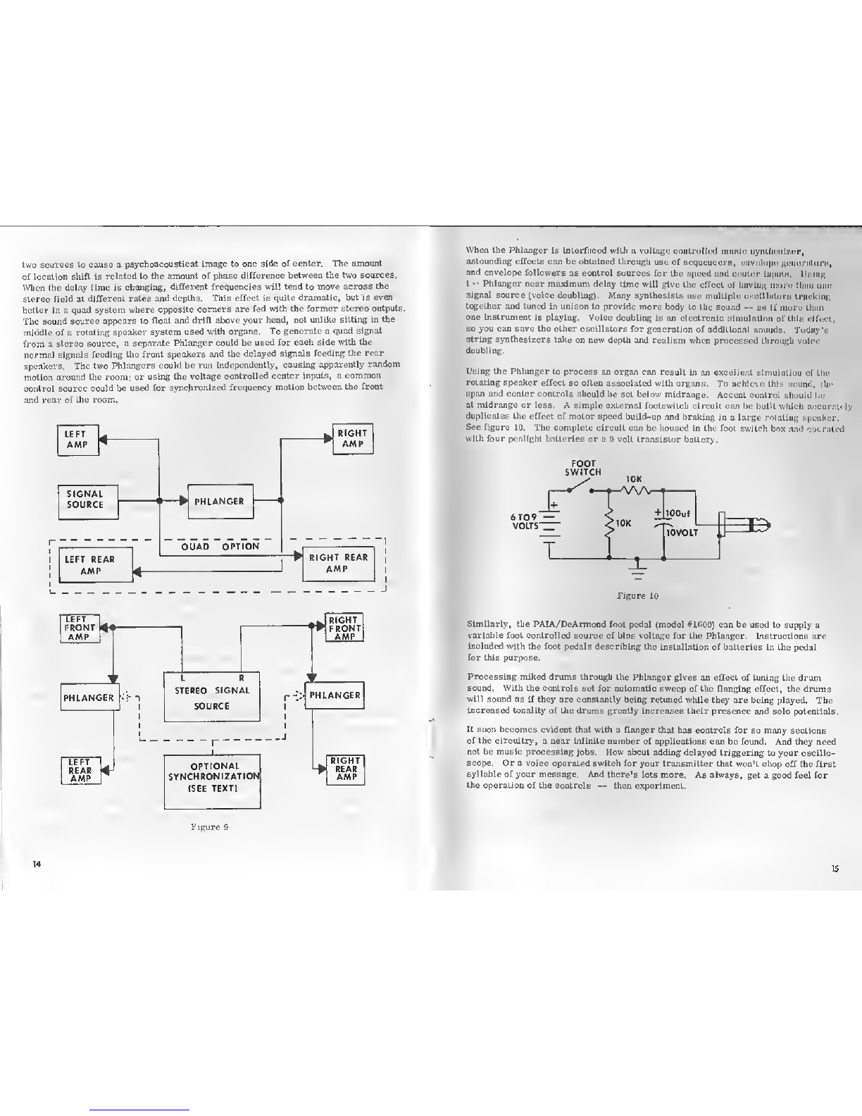
Another unique applicatton of the Phlanger is generation of stereo or quad motion
eSects from amono signal. See figure 9. For this effect, the original signal is
fed to Hie input of one amp AND to the Plilanger input. Tlie Phlanger output is then
fed to the remaining amp. Control settings on the Phlanger are the same as for
vibrato effects, except with aslov^r^ate. When asignal with complex harmonic
structure is fed flirmi^ this systCTO, some frefjoencies will be emitted from the
speakers In ^lase with each other. Ihe ai^iarent source of the sound will be between
the two speakers. Other frequencies will have enough phase dlKerence between the

two sources to cause apsychoacoustical image to one side of center. The amount
of location shift is related to the amount of phase difference between the two sources.
Wlien the delay time Is changing, different frequencies will tend to move across Uie
stereo field at different rates and depths. ThlB effect Is quite dramatic, but is even
better In aquad system where opposite-cornelTe axe&d witb the former stereo outputs.
The sound source appears to float and drift above your head, not unlikesitting in &e
middle of arotatii^ speaker system used w-ith organs. To generate a quad signal
f^'tU astereo sourco. ascjiaratc Phlangcr couki bo used for each side with the
.^^lil signaJs loediiii; the troiil speakers ^uicl the delayed sii^nals feeding the rear
speakers. The two Phlaagers could be run independently, causing appaa-cntly random
motion around tiie room; or using the voltage controlled center inputs, acommon
control source could be used for syncfironlzed frequency motion between the front
and rear of the room.
LEFT
AMP
SrCNAL
SOURCE PHLANGER
RIGHT
AMP
LEFT REAR
AMP
QUAD OPTION RIGHT REAR
AMP
FRONT
AMP
PHLANGER
LEFT
REAR
AMP
IR
STEREO SIGNAL
SOU I
r'
I
OPTIONAL
SYNCHRONIZATIO^
(SEE TEXT)
RIGHT
FRONT
AMP
PHLANGER
RIGHT
REAR
AMP
Figure S>^y .jaii>.
.1 ivftamu* .<ia o*-J
When the Pblanger is interiaced with avoltage oontrollod music NynlhoilEor,
astounding effects can be obtained through use of soquoDO«rB, oiwuldnn Ronornlnrs,
and envelope followers as control sources for the upood and ci-jiirj- lii|iui[,. itrijiiK
t<-• Phlanger near maximum delay time will give the effect oi IjiivIiik m-,y» i.liiuj unij
signal source (voice doubling). Many ayntheslsts use multiple uncllliit'irB li'iickinn
tog^Jier and tuned in unison to provide more body to the sound —-as Umore Uian
one Instrument Is pl^Flng. Voice doubling is an electronio simulation of Ihli offool;,
so you can save the other oscillators for generation of additional sounds, Today's
string synthesizers take on new depth and realism when processed through voire
doubling.
Using the Phlanger to process an organ can result In an excellent simulation of the
rotating speaker effccl so often associated with organs, To aehic\(: iliis Kound. ilio
span and cenLer controls should be set below mldrange. Accent control should Lit;
at midrange or less. Asimple external footswltch circuit can be bulU which aecuralcly
duplicates the effect of motor speed build-up and braking In alarge rotating speaker.
See figure 10. The complete circuit can be housed In the foot sv>-ltch box and optrstod
with four penlight batteries or a 9 volt transistor battery.
FOOT
SWITCH
Figuro 10
Similarly, the PAIA/DeArmond foot pedal (model #1R00) can be used to supply a
variable foot controlled source of bias voltage for the Phlanger, Instructions are
included with the foot pedals desoilblDg tlie Inatallatlon of batteries In the pedal
for this purpose.
Proceasing miked drums through the Phlanger gives an effect of tuning the drum
(sound. With the controls set for automatic sweep of the flanging effect, the drums
fwill sound as if they are constantly being retuned while they are being played. The
tr increaaed tonality of the drums greatly increases their presence and solo potentials.
It soon becomes evident that with afianger that has controls for so many sections
of the circuitrj', anear iniinite number of applications can be found. And they need
not be music processing jobs. How about adding delayed triggering to your osoiUo-
scope. Or avoice operated switch for your transmitter that won't chop off the first
syllable of your message. And there's lots more. As always, get agood feel for
^the operation of the controls —then experiment.
15

DESIGN ANALYSIS
The primary component lit the Pblanger is the Analog Delay Line IC. This device
iB new and special enou^ to WBrrauya^^ggciption of how it works and bow to ose
The Retlcon SAD-1024 is adual 512 stage analog sbifi register which represents
the third generation of analog del^ IC's. Beticon's use of N-channei technology
ellminatee the need for multiple supply lines, increases linearity and distortion
specs, improves i^namic range (S/N> 70db), and decreases loss. The SAD-1024
ulillKts MOS IranslsLora and capacitors in an array as shown In figure 11, The
;-cl«:iiia(.ic showK one ol' the two Identical circuiis contained in the IC. The circuit
]v\nu I':-- ;i I>i-|ilia;j0 clacking signal of ill and 02 {62 is the complement of 01) which
liab amiuiinum frequency of twice the highest frequency to be successfully passed
through the delay line. The clock signals should swing between Vdd and ground.
When il is bi^, the input Bignal is a^ilied to input capacitor Ce. At the moment
of clock transition, the input transiftor is dis^led and the voltage on Cs is froEeo.
With 0now high, the charge on Cs Is passed through abufier and onto the capaci-
tor In stage 1. The next time Hi is high, another sample of the input is lakcn and
Ultewlse passed down the chain of 509 bluraKo capacitors. AL the SlOlh stage the
signal is applied to two parallel shift registers, one having three stages and the
other having four stages. The signal will appear at output AS12 clock balf-periode
after it was applied to the input. The same output will swear at output Adiuring
the followins, or BUtb, cAtek half-period. This allows the output te be amore
ooattnuous ref^ssentttion.of the Input signal, and aids in suppressing residual
clodtlug glitcMe: Thus tlip time delay of Ute circuit can be figured by:
Tdj!(^S12/2F«wlwra Fc is tte freepuBcy onke-oloidE lines 01 and ^S.
Being astrict sampled data device viiirranls some dlrjrii; m, ,ji ul" i,aiii|ili(in ihnu'onia
^and special precaution;, which need to l>u tukoii. When t.:iiupliii|; ni\ iiiialui; ninnal,
confide ratj(jn must Ijc given to the numher of sajnples roqulrod to accurately re-
produce the original waveform. When the sample rate la 10 or more timea the
frequency of the input, the condition is known as overB"'nff')r>ff.This Is afavorable
condition, as the more samples taken per period yieU increasingly accurate re-
production of the input signal. As the input frequency is increased or the sample
rate Is decreased, fewer of the harmcniCG of the input signal will be reproduced
due to the inabilitj- of the sampling system to capture such rapid fluctuations. When
the input frequency aiiproaches half of the sample rate critical sampling occurs.
Only the fundamental sine wave will be reproduced from even the most complex
input waveforms. As the sample rate falls below twice the input frequency, drastic
distortion of both waveform and frequency will occur. This is called undersampUng
and, ezo^t for special applications, should be aralded. For most audio applications,
oversampling wltli apossible ai^roach to critical aampUog will be the operating
r^ion moat used.
To avoid modulation of the input signal against the clock frequency, the Input of a
delay system should have a low pass fUter whose coiner frequency is one-half to
pne-ttalrd the mtalmntn clock frequency. For audio nee, the Input signal will alroKdy
be limited, so as long as the clock remains above SOKHz no input fiUer will be required.
The output, however, will definitely need some type of Altering. Due to the sampled
nature of the delay chip output, the signal will at best be a^l:^^Klep approximation of
the Input signal. Also, there will be narrow plitches oc Hpikes riding on the waveform
which corresiwnd lo Ihc clock transitions eneountcri^d within Ihu delay chip. An oul^ut
wiach, like the input filter, is alow pass set at one-half or more of the minimum ol<jok
frequency wil 11) remove the residual clock signal, and 2) smooth the stairstep ilpprox-
Imation to anearly identical dupUcate of the orl^hal Input signal -except, of course,
delayed by Xamount of time. For audio use, an output filter at ISKHz with aminimum
olock rate of 30KBz is about as far as you want to posh it. Some audio fanatics may be
OODcemed about tUe setup having a maximum waveform recovery of asine wave at
ISKHz. But consider -primary fundajiK^Ual frequency content of most music Is only
up to about 4KHz. Energy distribution above this point consists primarily of harmonics
of the lower frequency waveforms. At I5KHz, these harmonics are running tens of "
db below the signal level of the fundamentals, and any loss is negligible.
The complete Phlanger schematic is etwwn in figure 6. The Input signal Is buffered
by ICIC and superimposed on a bias voltage determined by the setting of R6, For
proper operaticm of IC2, the bias must be set to 40% of the supply voltage. The output
of ICIC is fed to the hiputs of the dual delay line, IC2. Note that the clock signals
to each delay line are reversed, so iM Inr nnr line is 02 for the other. This is known
as parallel mulUplex operation and causes the input to be alternately sampled by the
two deli^ lines. The result Is that the input is sampled twice as many times per
period as with the normal mode of operation, and the output sifpal Is amore aoourate
represe&tatl<Hi of (be original input. One output from each delay line is applied to
the summing/balance network E6/R7. Accent control R8 selects the amount of delayed
signal to be fed back to the input for r^eneration. R9/C4, R10/C5, R11/C6 are low
pass filters used to remove the high frequency clock signal from the audio signal, and
to smooth the "staircase" sampled waveform Into aduplicate of the origtoal. Mixing
control R12 selects normal input, or delayed signal, or any blend of the two. The
mixed signal is amplified by ICIO to provide unity gain tbrougli the complete audio
Circuit.
17

The remaining two secHons of ICl comprise the low frequency triangle oscillator
used Lo sweep the flanging effect, ICIA forms an integrator whose slope is voltage
oiiLroUcd. Control voltage is derived from Speed control R17 or from remote input
J4 which is buffered by Ql. ICIB Is used as a Schmltt trigger which determined
whether the integrator wlll.^lopejwpitive or negative. Peak trimmer B2T fine tunes
the triangle output amplitude of K»1A for t^timom we with tbe fallowing drcnltir.
Span control R25 determines the amount of triangle signal used to modulate the hi^
frequency clock. As the span control is decreased, an Increasing amount of fixed
DC voltage is provided by Center control R26. AltornLileiy ,external control voltage
can be applied to Center jack J3 to set the initial high frequency clock rate. The
resultant mixed signal from this control network is available at the wiper of S|j:ui
control R25, and is applied to current source Q4. This current source replaces the
standard timing resistor for the VCO D34. WlQi the current range provided, the
frequency range of IC4 is applied to the clock Input of one of the D-type flip-flops
in IC3. This stage serves two purposes: dividing Oie clock signal by two, and
geiu' I'liting complonieiil:iry square wave outputs from the Qand Qoutputs. These
complementary signals drive the delay line clock inputs with afrequency range of
30KHZ to 500KHZ.
The power supply for the Phlanger is astandard full wave bridge rectifier with center
tap which provides ab^xtlar 9volt supply for the drcuitij.
.1 /-.-I K,1 ..f
u
i
Table of contents
Popular Adapter manuals by other brands

Addonics Technologies
Addonics Technologies NASU2 Quick install guide

National Instruments
National Instruments BNC-2110 installation guide

Patton electronics
Patton electronics 464RC user manual

Zonet
Zonet ZUN2200 Quick installation guide

Atop
Atop GW21W-MAXI user manual

Allen-Bradley
Allen-Bradley PowerFlex RS-485 DF1 user manual