8
4 Specifications
QProduct fiche
QOther information
Energy efficiency class B
Visible screen size (diagonal) 107 cm / 42 inches
On mode average power consumption 95 W
Annual energy consumption*1139 kWh
Rated power consumption 150 W
Standby power consumption*20.40 W
Off mode power consumption 0.30 W
Display resolution 1,024 (W) ×768 (H)
Power source AC 220-240 V, 50 / 60 Hz
Panel Plasma panel
Dimensions (W ×H ×D) 1,007 mm ×657 mm ×231 mm (With Pedestal)
1,007 mm ×615 mm ×81 mm (TV only)
Mass 17.5 Net (With Pedestal)
16.0 Net (TV only)
Sound
Speaker (160 mm ×40 mm) ×2, 8 Ω
Audio output 20 W (10 W + 10 W)
Headphones M3 (3.5 mm) stereo mini Jack ×1
Receiving systems / Band name
(UK) DVB-T / T2 Digital terrestrial services.
PAL I UHF E21-68
PAL 525/60 Playback of NTSC tape from some PAL Video recorders (VCR)
or NTSC disc playback from DVD player and recorder.
M.NTSC Playback from M.NTSC Video recorders (VCR).
NTSC (AV input only) Playback from NTSC Video recorders (VCR).
(Ireland)
DVB-T Digital terrestrial services.
PAL I VHF A -J
UHF E21-69
CATV S1 - S20
CATV S21 - S41 (Hyperband)
PAL 525/60 Playback of NTSC tape from some PAL Video recorders (VCR)
or NTSC disc playback from DVD player and recorder.
M.NTSC Playback from M.NTSC Video recorders (VCR).
NTSC (AV input only) Playback from NTSC Video recorders (VCR).
• Check the latest information on the available services at the following website.
http://panasonic.jp/support/global/cs/tv/
Aerial input UHF (UK) VHF / UHF (Ireland)
Operating conditions
Temperature: 0 °C- 35 °C
Humidity: 20 % - 80 % RH (non-condensing)
Connection terminals
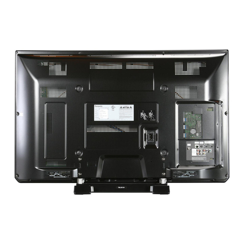
AV1 input / output SCART (Audio/Video in, Audio/Video out, RGB in, Q-Link)
AV2 input (COMPONENT /
VIDEO)
VIDEO: RCA PIN Type ×1 1.0 V [p-p] (75 Ω)
AUDIO L-R: RCA PIN Type ×2 0.5 V [rms]
Y: 1.0 V [p-p] (including synchronization)
PB, PR: ±0.35 V [p-p]
HDMI1 / 2 input TYPE A Connectors
HDMI1 : 3D, Content Type, Deep Colour, x.v.Colour™
HDMI2 : 3D, Content Type, Audio Return Channel, Deep Colour,
x.v.Colour™
• This TV supports [ HDAVI Control 5 ] function.
Card slot SD Card slot ×1
Common Interface slot (complies with CI Plus) ×1
ETHERNET RJ45, IEEE802.3 10BASE-T / 100BASE-TX
USB USB2.0 DC 5 V, Max. 500 mA
DIGITAL AUDIO OUT PCM / Dolby Digital / DTS, Fiber optic
*1: Energy consumption XYZ kWh per year, based on the power consumption of the television operating 4 hours per day for 365 days.
The actual energy consumption will depend on how the television is used.
*2: When the TV is turned off with the remote control and no function is active


