Panasonic PAN9420 Guide

PAN9420
Fully Embedded Stand-Alone Wi-Fi Module
Design Guide
Rev. 1.0
Wireless Modules

PAN9420 Wi-Fi Module
Design Guide Rev. 1.0 Page 2
Overview
The PAN9420 is a 2.4 GHz ISM band Wi-Fi
embedded module which includes a wireless radio
and an MCU for easy integration of
Wi-Fi connectivity into various electronic devices.
Features
•Fully embedded: integrated full-featured network
stack
•Contains all necessary IoT functionality (Place
and Play)
•Integrated web server with AJAX/JSON for
web applications
•No stack or software implementation needed on
a host MCU
•Simultaneous support of access point- and
Infrastructure mode
•Fully automatical IP configuration
•DHCP server offers IP configuration in AP mode
•Access by names (http://yourdevice)
•Integrated TCP/IP network stack: IPv4, ARP,
and Auto IP
•Supports TLS/SSL, HTTPS and Wi-Fi security
(WPA2-PSK) for secure data connection
Over-the-Air firmware update
•Two UART interfaces (command and
transparent data)
•Integrated QSPI flash memory for customer
web contents and configuration file
•Programming via standard JTAG
•Evaluation kit with pre-installed web application
for quick prototyping available
•Evaluation and development tool WiFigurator for
Windows
•Getting started tutorials, PC tool,
Quick Start Guide
•Wide temperature range of -40 °C to +85 °C
Characteristics
•Surface Mount Type (SMT)
29.0 mm x 13.5 mm x 2.66 mm
•Marvell® 88MW300 MCU/WLAN
System-on-Chip (SoC) inside
•Tx power up to +16 dBm @ IEEE 802.11b
•Rx sensitivity of -97 dBm @ IEEE 802.11b DSSS
1 Mbps
•20 MHz channels up to 72 Mbps
•Power supply 3.0 V-3.6 V
•Current consumption 150 mA (mix mode
Tx/Rx @ 11b, 11 Mbps), 75 mA Rx, 310 mA Tx
peak
•Power down mode < 1 mA power consumption
•Low power mode available
Block Diagram
Chip
Antenna
SPDT
88MW300
MCU/Radio SoC
Crystal
32.768 kHz
QSPI Flash
32 Mbit
SPI
UART0
UART1
GPIOs
Status LEDs
MCU Ready
Resetn
Factory Reset
V SPDT
Wake Ups
JTAG
Vcc 3.3 V
LPF
RF-Pad
PAN9420
Fully Embedded Wi-Fi Module
IEEE 802.11 b/g/n
Crystal
38.4 MHz

PAN9420 Wi-Fi Module
Design Guide Rev. 1.0 Page 3
By purchase of any of the products described in this document the customer accepts the document's
validity and declares their agreement and understanding of its contents and recommendations. Panasonic
Industrial Devices Europe GmbH (Panasonic) reserves the right to make changes as required at any time
without notification. Please consult the most recently issued Design Guide before initiating or completing a
design.
© Panasonic Industrial Devices Europe GmbH 2018.
This specification sheet is copyrighted. Reproduction of this document is permissible only if reproduction is
without alteration and is accompanied by all associated warranties, conditions, limitations, and notices. Do
not disclose it to a third party.
All rights reserved.
This Design Guide does not lodge the claim to be complete and free of mistakes.
Engineering Samples (ES)
If Engineering Samples are delivered to the customer, these samples have the status “Engineering
Samples”. This means that the design of this product is not yet concluded. Engineering Samples may be
partially or fully functional, and they may differ from the published Product Specification.
Engineering Samples are not qualified and they are not to be used for reliability testing or series
production.
Disclaimer
The customer acknowledges that samples may deviate from the Design Guide and may bear defects due
to their status of development and the lack of qualification mentioned above.
Panasonic rejects any liability or product warranty for Engineering Samples. In particular, Panasonic
disclaims liability for damages caused by:
The use of the Engineering Sample other than for evaluation purposes, particularly the installation
or integration in another product to be sold by the customer,
Deviation or lapse in function of the Engineering Sample,
Improper use of the Engineering Sample.
Panasonic Industrial Devices Europe GmbH disclaims any liability for consequential and incidental
damages. In case of any queries regarding the Engineering Samples, please contact your local sales
partner or the related product manager.

PAN9420 Wi-Fi Module
Design Guide Rev. 1.0 Page 4
Table of Contents
1About This Document.........................................................................................................................5
1.1 Purpose and Audience ..............................................................................................................5
1.2 Revision History.........................................................................................................................5
1.3 Use of Symbols .........................................................................................................................5
1.4 Related Documents...................................................................................................................5
2Overview..............................................................................................................................................6
3PAN9420 Module.................................................................................................................................7
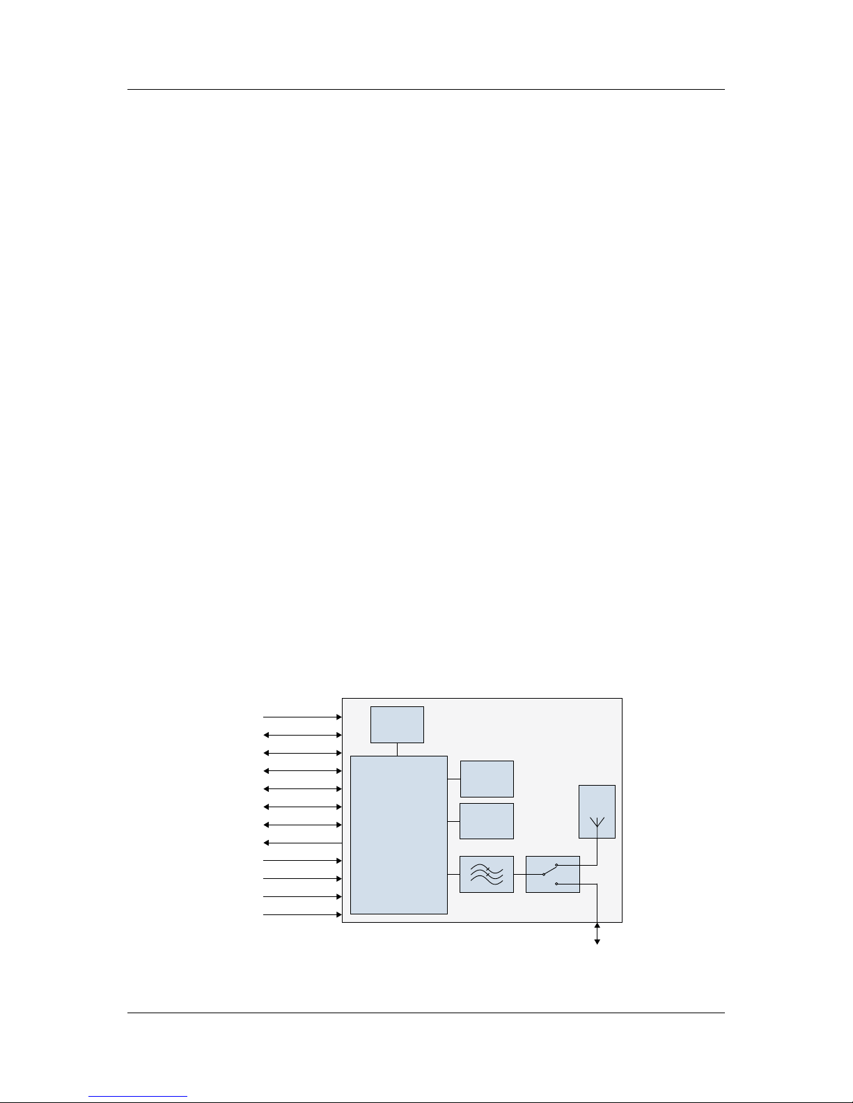
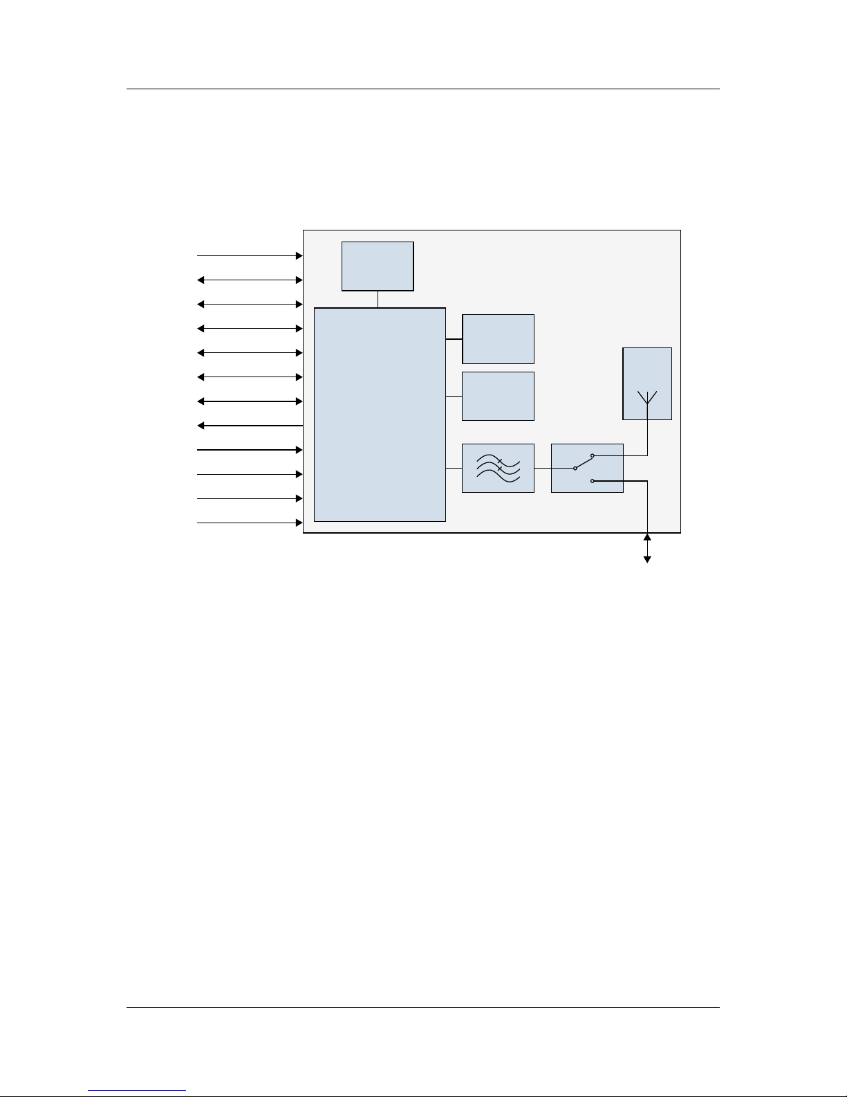
3.1 Block Diagram...........................................................................................................................7
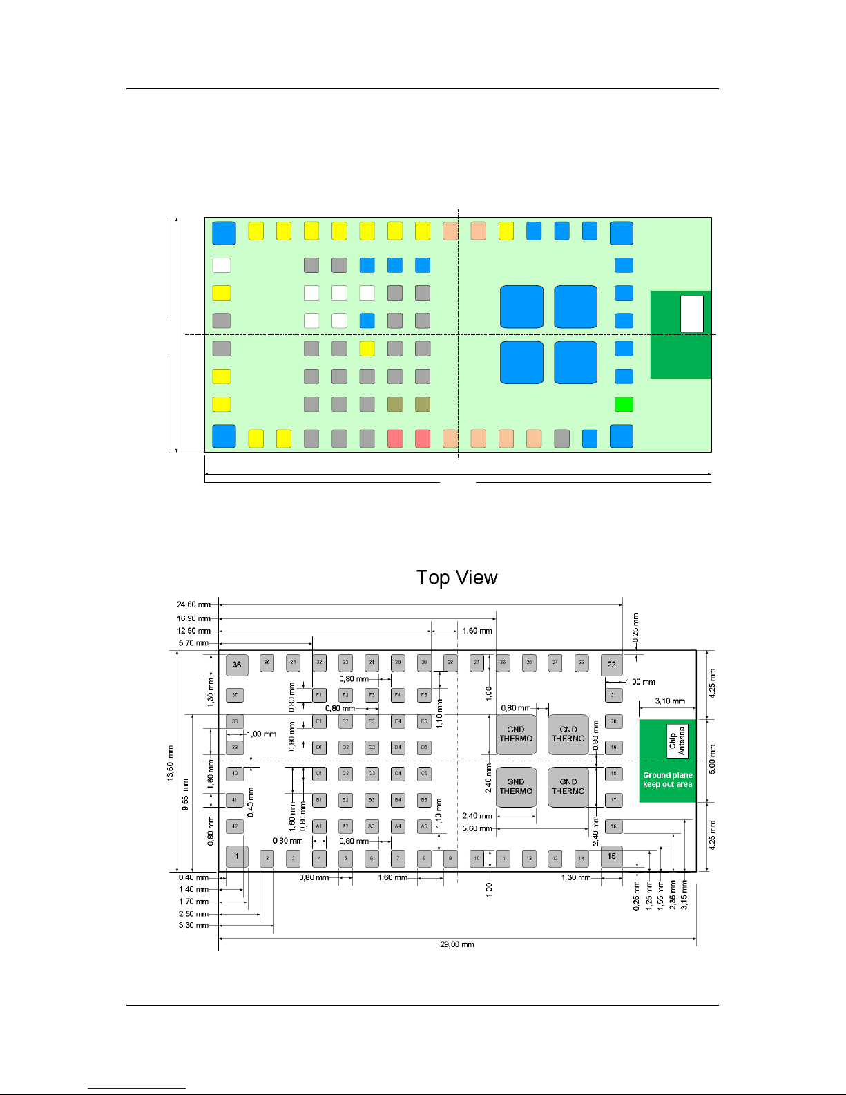
3.2 Footprint ....................................................................................................................................8
3.3 Land Pattern..............................................................................................................................8
3.4 Pattern Recommendation..........................................................................................................9
3.5 Solder and Resist Mask.............................................................................................................9
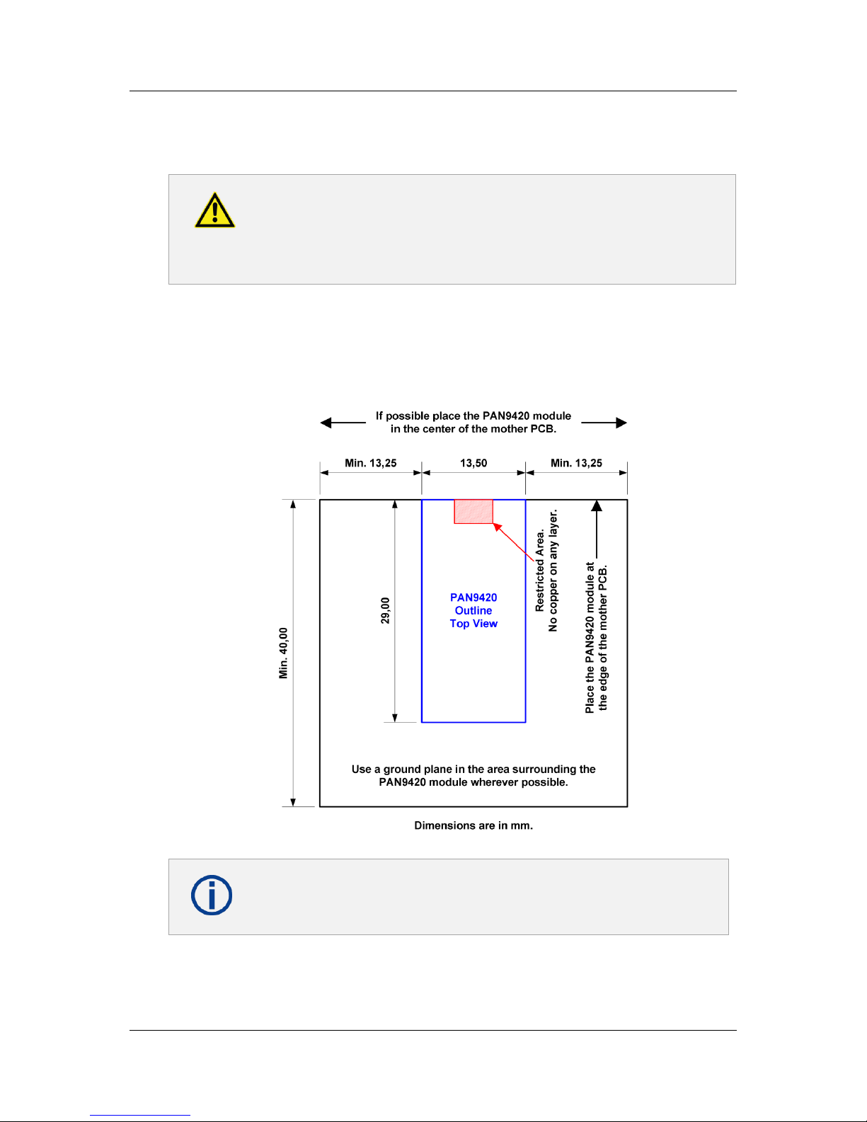
3.6 Placement................................................................................................................................10
3.7 Power Supply ..........................................................................................................................11
3.8 RF Path ...................................................................................................................................11
4PAN9420ETU (Easy-To-Use)............................................................................................................14
4.1 PAN9420ETU Live View..........................................................................................................14
4.2 Functional Blocks ....................................................................................................................15
4.3 Pinning.....................................................................................................................................16
4.4 Part Placement........................................................................................................................18
4.5 Schematic................................................................................................................................19
4.6 PCB Layout .............................................................................................................................20
5PAN9420 Arduino Shield..................................................................................................................22
5.1 PAN9420 Arduino Shield Live View.........................................................................................22
5.2 Functional Blocks ....................................................................................................................23
5.3 Pinning.....................................................................................................................................24
5.4 Part Placement........................................................................................................................24
5.5 Schematic................................................................................................................................25
5.6 PCB Layout .............................................................................................................................26
6Cautions ............................................................................................................................................27
6.1 Life Support Policy...................................................................................................................27
7Appendix ...........................................................................................................................................28
7.1 Ordering Information................................................................................................................28
7.2 Contact Details........................................................................................................................29

PAN9420 Wi-Fi Module
1 About This Document
Design Guide Rev. 1.0 Page 5
1 About This Document
1.1 Purpose and Audience
This Design Guide provides details on the electrical integration of the Panasonic PAN9420
module. It is intended for hardware design, application, and Original Equipment Manufacturers
(OEM) engineers. The product is referred to as “the PAN9520” or “the module” within this
document.
1.2 Revision History
Revision
Date
Modifications/Remarks
1.0
2018-07-17
First Design Guide version
1.3 Use of Symbols
Symbol
Description
Note
Indicates important information for the proper use of the product.
Non-observance can lead to errors.
Attention
Indicates important notes that, if not observed, can put the product’s functionality
at risk.
Tip
Indicates useful information designed to facilitate working with the PAN9420.
[chapter number]
[chapter title]
Cross reference
Indicates cross references within the document.
Example:
Description of the symbols used in this document 1.3 Use of Symbols.
Requirement
Indicates a requirement that must be met before the corresponding tasks can be
completed.
1.4 Related Documents
Please refer to the Panasonic website for related documents 7.2.2 Product Information.

PAN9420 Wi-Fi Module
2 Overview
Design Guide Rev. 1.0 Page 6
2 Overview
This Design Guide applies to the PAN9420 Wi-Fi embedded module and the PAN9420ETU
(Easy-To-Use) development platform. The intention is to enable our customers to easily and
fast integrate our module PAN9420 in their product. This Design Guide describes the hardware
integration and gives useful hints.
This document is structured into two main parts:
•The hardware integration of the PAN9420 module.
•The PAN9420ETU development platform as an example for the module integration.
Please refer to the Panasonic website for related documents 7.2.2 Product Information.
Further information on the variants and versions 7.1 Ordering Information.

PAN9420 Wi-Fi Module
3 PAN9420 Module
Design Guide Rev. 1.0 Page 7
3 PAN9420 Module
3.1 Block Diagram
Chip
Antenna
SPDT
88MW300
MCU/Radio SoC
Crystal
32.768 kHz
QSPI Flash
32 Mbit
SPI
UART0
UART1
GPIOs
Status LEDs
MCU Ready
Resetn
Factory Reset
V SPDT
Wake Ups
JTAG
Vcc 3.3 V
LPF
RF-Pad
PAN9420
Fully Embedded Wi-Fi Module
IEEE 802.11 b/g/n
Crystal
38.4 MHz

PAN9420 Wi-Fi Module
3 PAN9420 Module
Design Guide Rev. 1.0 Page 8
3.2 Footprint
GND GND
29,00 mm
13,50 mm
Top View PAN9420
GNDGND
NC
(RF)
GND
GND
GND
GND
GND
FACTORY
RESET
MCU
READY
RESETn
Chip
Antenna
NC
WPDn
NC
W
RESETnGND GND GND
TDO TCK TMS QSPI
D2 NC
QSPI
CS
TDI TRSTn NC
(GND) QSPI
D0 QSPI
D1
NC NC WAKE
UP1 QSPI
CLK QSPI
D3
NC BT
FREQ BT
GRANT BT
REQ BT
STATE
NC NC NC
NC 3.3V 3.3V UART1
CTSn UART1
RTSn UART1
TXD UART1
RXD QSPI
CS2 GND
STAT
LED2 STAT
LED1
STAT
LED3 UART0
RXD UART0
TXD
W
STAT
LED GND GND GND
GND
THERMO GND
THERMO
GND
THERMO GND
THERMO
NC
NC
BOOT2
NC
BOOT1
WAKE
UP0
NC
NC
NC NC NC NC
NC NC
SPDT
V2
SPDT
V1
GPIO
49
GPIO
48
GPIO
47
GPIO
46
GPIO
4
GPIO
5
46 47 48 49
BT
REQ
NC BT
REQ
NC
BT
REQ
NC BT
REQ
NC
BT
REQ
NC
BT
REQ
NC
3.3 Land Pattern

PAN9420 Wi-Fi Module
3 PAN9420 Module
Design Guide Rev. 1.0 Page 9
3.4 Pattern Recommendation
Note:
If the module is used with
the internal ceramic chip
antenna the gray marked
area of module antenna
area ( 5,0 x 3,1 mm2 ) and
the right side of mother
PCB edge are restricted.
Means no ground plane,
no signal pattern and in
general no metal should
be placed.
min. 15 mm
min. 15 mm
Note:
If the module is used with
the internal ceramic chip
antenna, the blue marked
area should be used to
place a ground plane.
36 22
29,00 mm
13,50 mm
Top View
151
3,10 mm
17
18
19
20
21
42
41
40
39
38
37
Chip
Antenna
F1 F2 F3 F4 F5
Pad Type 1 = 4 x 1.30mm x 1.30mm
Pad Type 2 = 38 x 0.80mm x 1.00mm
Pad Type 3 = 30 x 0.80mm x 0.80mm
E1 E2 E3 E4 E5
D1 D2 D3 D4 D5
C1 C2 C3 C4 C5
B1 B2 B3 B4 B5
A1 A2 A3 A4 A5
2 3 4 5 6 7 8 9 10 11 12 13 14
35 34 33 32 31 30 29 28 27 26 25 24 23
5.0 mm
Mother PCB edge
16
PCB footprint recommendation
Pattern land same land dimension as module pad type
Resist mask 50µm bigger land size as pad type to each direction
GND
THERMO GND
THERMO
GND
THERMO GND
THERMO
Mother PCB edge
Pad Type 4 = 4 x 2.40mm x 2.40mm
Pin 16 - RF
50 Ohm RF pad for the
connection to an external
antenna
It is recommended to extend
the ground plane for module
to get best RF characteristic
and heat rejection condition.
3.5 Solder and Resist Mask
The following requirements must be met:
The Resist Mask should be circumferential 50 µm bigger than the pad size (3.3 Land
Pattern).
The Solder Mask apertures should have the diameter as the pads (3.3 Land Pattern);
they are separated in two parts with the shown distance and a shifting.

PAN9420 Wi-Fi Module
3 PAN9420 Module
Design Guide Rev. 1.0 Page 10
3.6 Placement
Antenna Keep-out Area
Do not place any ground plane under the marked restricted antenna area in
any layer! This would be affecting the performance of the chip antenna in a
critical manner.
The following requirements must be met:
Keep this product away from heat. Heat is the major cause of decreasing the life of these
products.
Keep this product away from other high frequency circuits.
The above recommendation for the ground plane is based on a FR4 4-Layer
PCB.

PAN9420 Wi-Fi Module
3 PAN9420 Module
Design Guide Rev. 1.0 Page 11
Impact of Placement on the Antenna Radiation Pattern
The placement of the module, the surrounding material, and the customer
components might have an impact on the radiation pattern of the on-board
antenna.
It is recommended to verify the perfect position of the module in the target
application before fixing the design. In some applications it could be
reasonable to use an external antenna to handle application caused
placement restrictions.
For the use of an external antenna refer to section 3.8.1 External Antenna.
3.7 Power Supply
The following requirements must be met:
The supply voltage must be free of AC ripple voltage (for example from a battery or a low
noise regulator output). For noisy supply voltages, provide a decoupling circuit (for example
a ferrite in series connection and a bypass capacitor to ground of at least 47 µF directly at
the module).
The supply voltage should not be exceedingly high or reversed. It should not carry noise
and/or spikes.
Make sure that the power-up sequence meets the requirements mentioned in the PAN9420
Product Specification.
The supply current of VDD (3.3V) must be limited to maximal 1 A.
3.8 RF Path
3.8.1 External Antenna
Antenna Warning
The PAN9420 is tested with a standard U.FL connector and with the antenna
listed in the regulatory and certification chapter of the PAN9420 Product
Specification. When integrated into the OEM’s product, these fixed antennas
require installation preventing end users from replacing them with
non-approved antennas. Any antenna not in the regulatory and certification
chapter of the PAN9420 Product Specification must be tested to comply with
FCC Section 15.203 for unique antenna connectors and with Section 15.247
for emissions.
The PAN9420 module has a 50 RF pin (SMD pad). Connect an external antenna directly or
via a connector (e.g. U.FL) with RF trace to this RF pin. This RF trace shall be matched to 50
3.8.2 RF Trace.

PAN9420 Wi-Fi Module
3 PAN9420 Module
Design Guide Rev. 1.0 Page 12
3.8.2 RF Trace
Ensure that the RF trace impedance is nearly 50 . It is recommended to use a Coplanar
Waveguide with Ground (CPWG) design. The impedance is related to the trace width, the
distances of the trace to the ground layers and the material of the PCB.
The following requirements shall be met:
Trace impedance of 50
Trace length shall not exceed 2 cm
Via fence around the trace
Crossing no other lines (power supply, interfaces or clock traces)
Example 1: 50 Coplanar Waveguide with Ground on SDIO Adapter
Trace width
Trace distance to ground
Substrate thickness
Effective Permittivity
Loss Tangent
W = 180 µm
S = 150 µm
H = 80 µm
𝜀𝑟 = 3.9
tan 𝛿 = 0.015

PAN9420 Wi-Fi Module
3 PAN9420 Module
Design Guide Rev. 1.0 Page 13
Example 2: 50 Coplanar Waveguide with Ground and Micro Vias
Trace width
Trace distance to ground
Substrate thickness
Effective Permittivity
Loss Tangent
W = 300 µm
S = 300 µm
H = 160 µm
𝜀𝑟 = 4.2
tan 𝛿 = 0.006

PAN9420 Wi-Fi Module
4 PAN9420ETU (Easy-To-Use)
Design Guide Rev. 1.0 Page 14
4 PAN9420ETU (Easy-To-Use)
The PAN9420ETU (Order-No. ENW49C01AZKF) is a sample application of the PAN9420
module. It is designed for mounting on the PAN9420 mother board
(Order-No. ENW49C01AYKF)
4.1 PAN9420ETU Live View
4.1.1 PAN9420 Mother Board Live View
For further information of the PAN9420 mother board please refer to the
PAN9420 Quick Start Guide 7.2 Contact Details.

PAN9420 Wi-Fi Module
4 PAN9420ETU (Easy-To-Use)
Design Guide Rev. 1.0 Page 15
4.2 Functional Blocks
Functional Block
Description
A
Vcc LED (is active when Vcc is supplied)
B
Reset button
C
Status LED’s
D
PAN9420 module
E
On-board antenna or U.FL connector selection
F
U.FL connector
D
F
E
A
B
C

PAN9420 Wi-Fi Module
4 PAN9420ETU (Easy-To-Use)
Design Guide Rev. 1.0 Page 16
4.3 Pinning
Pin Functions
Pin
Header
Pin No.
Related
Module Pin
Pin Name
Description
JP1
1
Ground
Connect to ground
2
-
-
-
3
42
FACTORY RESET
Factory reset (valid after 10 seconds), active high
4
-
-
-
5
38
WAKE UP0
Wake up signal for MCU/WLAN SoC, active high
6
C3
WAKE UP1
Wake up signal for MCU/WLAN SoC, active high
7
-
-
-
8
9
UART1 CTS
CTSn for UART1 (using hardware flow control)
9
10
UART1 RTS
RTSn for UART1 (using hardware flow control)
10
11
UART1 TXD
TXD for UART1
11
12
UART1 RXD
RXD for UART1
12
Ground
Connect to ground
JP2
X3
1
1
1
1JP1
X2 X1

PAN9420 Wi-Fi Module
4 PAN9420ETU (Easy-To-Use)
Design Guide Rev. 1.0 Page 17
Pin
Header
Pin No.
Related
Module Pin
Pin Name
Description
JP2
1
Ground
Connect to ground
2
37
RESETn
Reset MCU, active low
3
7, 8
3.3 V
3.0 V-3.6 V power supply (typical 3.3 V)
4
7, 8
3.3 V
3.0 V-3.6 V power supply (typical 3.3 V)
5
D1
TDI
TDI for JTAG
6
E1
TDO
TDO for JTAG
7
E2
TCK
TCK for JTAG
8
E3
TMS
TMS for JTAG
9
D2
TRSTn
TRSTn for JTAG
10
28
UART0 RXD/DUAL
SW
RXD for UART0/UART1 toggle switch for the
control of the state
11
27
UART0 TXD/DUAL
STAT
TXD for UART0/UART1 state (binary data or
command)
12
Ground
Connect to ground
X1
16
NC/RF
RF in/out over 50Ω bottom pad
X2
1
2
GPIO4
Digital I/O #4
2
3
GPIO5
Digital I/O #5
3
Ground
Connect to ground
X3
1
29
GPIO49
Digital I/O #49
2
30
GPIO48
Digital I/O #48
3
31
GPIO47
Digital I/O #47
4
32
GPIO46
Digital I/O #46
5
-
-
-
6
41
MCU READY
MCU ready (booting ready), active high
7
Ground
Connect to ground

PAN9420 Wi-Fi Module
4 PAN9420ETU (Easy-To-Use)
Design Guide Rev. 1.0 Page 18
4.4 Part Placement
MOD1
R6 R7
LED2
LED3
R8 R10
LED4
LED5
R2 R3 R4 R5C1 R13
R9 C3
R15
LED6
R1'
X2
X3
S1
JP1
JP2
LED1
R1
C2
S4
R2'
R17
R18
R19
R20
X1
R21
R22
R23

PAN9420 Wi-Fi Module
4 PAN9420ETU (Easy-To-Use)
Design Guide Rev. 1.0 Page 19
4.5 Schematic
BOOT1 BOOT1 Boot from
1 1
0 0 UART
QSPI
SPDT_U1 SPDT_U2 Output
HIGH LOW
LOW HIGH Connector
Antenna
GND
+3V3
PAN9420
GND
680
680
GREEN
YELLOW 680
680
RED
BLUE
+3V3
10k
10k
10k
10k
0.1
GND
10k
GND
+3V3
GND 10k
+3V3
0.1
GND
680
WHITE
GND
1.8k, n.c.
GND
GND
GND
B3U-1000P
GREEN
680
GND
GND
1µ
GND
+3V3
GND
ALPS_SSSS810701
1,8k, n.c.
GND
+3V3
10k
n.c.
n.c.
10k
GND
+3V3
GND
GND
GND
0R
NC
NC
MOD1
GND
1
GND
14
GND
15
GND
17
GND
18
GND
19
GND
20
GND
21
GND
22
GND
23
GND
24
GND
25
GND
36
GND
F3
GND
F4
GND
F5
GND
D3
GND_THERMO
T1
GND_THERMO
T2
GND_THERMO
T3
GND_THERMO
T4
GPIO[4]_/_I2C0_SDA
2
GPIO[5]_/_I2C0_SCL
3
3.3V 7
3.3V 8
UART1_CTSN
9UART1_RTSN
10
UART1_TXD
11
UART1_RXD
12
RF 16
W_STATUS_LED
26
UART0_TXD
27
UART0_RXD
28
GPIO[16]_/_BOOT1 5
GPIO[27]_/_BOOT2 6
GPIO[46]_/_SSP2_CLK
32 GPIO[47]_/_SSP2_FRM
31
STATUS_LED3
35 STATUS_LED2
34 STATUS_LED1
33
RESETN
37
WAKE_UP0
38
GPIO[48]_/_SSP2_TXD
30
MCU_READY
41
FACTORY_RESET
42
WAKE_UP1
C3
QSPI_CLK C4
QSPI_D3 C5
TDI D1
TRSTN D2
QSPI_D0 D4
QSPI_D1 D5
TDO E1
TCK E2
TMS E3
QSPI_D2 E4
QSPI_CS E5
GPIO[49]_/_SSP2_RXD
29
SPDT_U2 A5
SPDT_U1 A4
R6
R7
LED2
LED3 R8
R10
LED4
LED5
R2
R3
R4
R5
C1
R13
R9
C3
R15
LED6
R1'
X2
1
2
3
X3
1
2
3
4
5
6
7
S1
JP1
1
2
3
4
5
6
7
8
9
10
11
12
JP2
1
2
3
4
5
6
7
8
9
10
11
12
LED1
R1
C2
S4
R2'
R17
R18
R19
R20
R21
R22
R23
UART0_TXD
UART0_TXD
UART0_RXD
UART0_RXD
UART1_TXD
UART1_TXD
UART1_RXD
UART1_RXD
UART1_RTS
UART1_RTS
UART1_CTS
UART1_CTS
RESETN
RESETN
RESETN
MOD_TDI
MOD_TDI
MOD_TDO
MOD_TDO
MOD_TCK
MOD_TCK
MOD_TMS
MOD_TMS
MOD_TRSTN
MOD_TRSTN
S3
S3
S4
S4
S1
S1
MCU_READY
MCU_READY
GPIO[49]
GPIO[49]
GPIO[48]
GPIO[48]
GPIO[47]
GPIO[47]
GPIO[46]
GPIO[46]
GPIO[4]
GPIO[4]
GPIO[5]
GPIO[5]
GPIO[27]_/_BOOT2
GPIO[27]_/_BOOT2
GPIO[16]_/_BOOT1
GPIO[16]_/_BOOT1
SPDT_U1
SPDT_U1
SPDT_U2
SPDT_U2
V1.0
U$1

PAN9420 Wi-Fi Module
4 PAN9420ETU (Easy-To-Use)
Design Guide Rev. 1.0 Page 20
4.6 PCB Layout
4.6.1 Top Layer
4.6.2 Layer 2
Other manuals for PAN9420
2
Table of contents
Other Panasonic Wireless Router manuals

Panasonic
Panasonic PAN9420 Owner's manual

Panasonic
Panasonic KX-TGA915EX User manual

Panasonic
Panasonic KX-TGA575C User manual

Panasonic
Panasonic ET-WM300 User manual

Panasonic
Panasonic KX-TGA595AL User manual

Panasonic
Panasonic KX-TDE600 Owner's manual

Panasonic
Panasonic PAN9520 Quick setup guide

Panasonic
Panasonic KX-TGA575 User manual
Popular Wireless Router manuals by other brands

Linksys
Linksys WRT54G2 - Wireless-G Broadband Router user guide

Aluratek
Aluratek CDW530AMF Product reference sheet

TP-Link
TP-Link TL-WPA4220T Quick installation guide

NETGEAR
NETGEAR WNR612 - Wireless-N 150 Router user manual

Moxa Technologies
Moxa Technologies AWK-4131 Hardware installation guide

Linksys
Linksys WRTP54G-ER Product data