PC Engines ALIX.2 Series User manual

PC Engines
ALIX.2 / ALIX.3 series
system boards

ALIX system board 2 1/15/2008
2007 PC Engines GmbH. A rights reserved.
PC Engines GmbH
www.pcengines.ch
tinyBIOS and PC Engines are trademarks of PC Engines GmbH.
A other marks and brands are property of their respective owners.

ALIX system board 3 1/15/2008
Table of contents
Federa Communications Commission Statement 4
CE Dec aration of Conformity 4
Comp iance information 5
Recyc ing / disposa 5
Introduction / features 6
OEM options 6
ALIX.2 series 7
ALIX.3 series 8
Getting started… 9
Setup options 9
PXE boot 10
Power over Ethernet 10
Known issues 10
Operating system compatibi ity 11
FreeBSD 11
FreeDOS, MS-DOS 5.0 11
Linux 11
NetBSD 11
OpenBSD 11
ALIX b ock diagram 12
ALIX connector pinouts 13
Status LEDs 18
Mode switch 18
BIOS POST codes 19

ALIX system board 4 1/15/2008
Federal Communications Commission Statement
This device comp ies with Part 15 of the FCC Ru es. Operation is subject to the fo owing two
conditions: (1) this device may not cause harmfu interference, and (2) this device must accept any
interference received, inc uding interference that may cause undesired operation.
This equipment has been tested and found to comp y with the imits for a C ass B digita device,
pursuant to Part 15 of the FCC Ru es. These imits are designed to provide reasonab e protection
against harmfu interference in a residentia insta ation. This equipment generates, uses and can
radiate radio energy. If this equipment is not insta ed and used in accordance with the
manufacturer’s instructions, it may cause harmfu interference to radio communications. However,
there is no guarantee that interference wi not occur in a particu ar insta ation. If this equipment
does cause harmfu interference to radio or te evision reception, which can be determined by
turning the equipment off and on, the user is encouraged to correct the interference by one or more
of the fo owing measures:
•Reorient or re ocate the receiving antenna.
•Increase the separation between the equipment and receiver.
•Connect the equipment to an out et on a circuit different from that to which the receiver is
connected.
•Consu t the dea er or an experienced radio/TV technician for he p.
This board is designed for insta ation in a shie ded enc osure (meta or p astic with conductive
coating). Shie ded cab es are required on LAN and seria ports to assure comp iance with FCC
regu ations.
A copy of the test report wi be provided on request.
CE Declaration of Conformity
We, PC Engines GmbH, dec are that ALIX.2 and ALIX.3 series boards, when insta ed in PC
Engines meta enc osures. (case1c1 / case1c2 / box2c), are in conformance with:
-EN 61000-6-3 (2005) (emissions, residentia and industria )
-EN 61000-6-2 (ESD, susceptibi ity, residentia and industria )
The unit under test is in conformity with the standards mentioned above. A copy of the test report
wi be provided on request.

ALIX system board 5 1/15/2008
Compliance information
For FCC, ALIX has been tested as a CPU board, insta ed in an enc osure, with the top cover
removed. No further testing shou d be required if the board is used with other FCC tested modu ar
components. P ease see http://www.fcc.gov/oet/ for more detai s. The responsib e party for FCC is
the importer.
Testing for CE mark must be done at the eve of the comp ete product, possib y inc uding the
wire ess cards. P ease contact PC Engines for assistance and documentation.
For satisfactory resistance to e ectrostatic discharge events (ESD), the ALIX board shou d be
grounded (e.g. through the mounting ho es, or the seria port connector). The USB port on
ALIX.2B / ALIX.3B boards is sensitive to ESD events, spurious overcurrent events may be
detected in this version.
Recycling / disposal
Do not discard e ectronic products in househo d trash!
A waste e ectronics equipment shou d be recyc ed according to oca regu ations.
Information for t e recycler:
Cut off Lithium battery, if present, for separate recyc ing.
PC Engines enc osures are made of a uminium.

ALIX system board 6 1/15/2008
Introduction / features
ALIX.2 and ALIX.3 are sma form factor system boards optimized for wire ess routing and
network security app ications.
•AMD Geode LX CPU, 433 Mhz (LX700) or 500 MHz (LX800) 5x86 CPU,
•256 KB cache (64K data + 64K instruction + 128K L2)
•1 to 3 Ethernet channe s (Via VT6105M, 10 / 100 Mbit/s)
•1 or 2 miniPCI sockets for 802.11 wire ess cards and other expansion
•128 or 256 MB DDR SDRAM, 64 bit wide for high memory bandwidth
•512 KB f ash for PC Engines tinyBIOS
•CompactF ash + optiona 44 pin IDE header for user’s operating system and app ication
•7 to 18V (abso ute maximum) DC supp y through DC jack or passive power over Ethernet
•1 seria port (DB9 ma e)
•2 USB 2.0 ports (optiona )
•Header for LPC bus (use for f ash recovery or I/O expansion)
OEM options
The fo owing options can be configured for arger orders:
•DRAM size (128 MB, 256 MB)
•CPU speed (LX700 / LX800 / LX900)
•De ete I/O not required by customer
•CMOS eve seria port (RXD / TXD on y)
•Optiona header for I2C bus
•Optiona buzzer for “beeps”
•Optiona RTC battery
•ALIX.3: optiona AC97 audio codec (headphone + mic)
•ALIX.3: optiona VGA video
•ALIX3: optiona pushbutton switch
•PC Engines tinyBIOS

ALIX system board 7 1/15/2008
ALIX.2 series
Configuration 2 LAN / 2 miniPCI, or 3 LAN / 1 miniPCI
Power supp y 7 to 20V DC, about 3 to 4W at Linux id e, peak about 6W without
miniPCI cards and USB devices. Suggest a 18V / 15W supp y. Center pin =
positive, s eeve = ground, 2.1 mm diameter.
Temperature range 0 to 50°C.
Dimensions 6 x 6” (152.4 x 152.4 mm)
ALIX system board 8 1/15/2008
ALIX.3 series
Configuration 1 LAN / 2 miniPCI
Power supp y 7 to 20V DC, about 2.5 to 3.5W at Linux id e, peak about 5W without
miniPCI cards and USB devices. Suggest a 18V / 15W supp y. Center pin =
positive, s eeve = ground, 2.1 mm diameter.
Temperature range 0 to 50°C.
Dimensions 100 x 160 mm

ALIX system board 9 1/15/2008
Getting started…
-Insta a bootab e CF card. Hot swap of CF cards is not supported!
-Connect seria port to a PC through nu modem cab e (RXD / TXD crossed over). Set termina
emu ator to 38400 8N1, f ow contro = none or xon-xoff.
-Connect Ethernet as needed.
-Connect a 18V DC power supp y to the DC jack. Power supp y shou d be ab e to supp y at east
12W for some margin. To avoid arcing, p ease p ug in the DC jack first, then p ug the adapter
into mains.
The board shou d now power on. A three LEDs wi ight during BIOS POST, then the system wi
try to boot, and turn off two of the LEDs.
You shou d see tinyBIOS startup messages, memory size, CF disk geometry on the seria conso e.
Setup options
To enter setup, type S during the memory test. You shou d see something ike the fo owing:
PC Engines ALIX.2 v0.98j
640 KB Base Memory
261120 KB Extended Memory
01F0 Master 848A CF 128MB
Phys C/H/S 1002/8/32 Log C/H/S 1002/8/32
BIOS setup:
(9) 9600 baud (2) 19200 baud *3* 38400 baud (5) 57600 baud (1) 115200 baud
*C* CHS mode (L) LBA mode (W) HDD wait (V) HDD slave (U) UDMA enable
(M) MFGPT workaround
(P) late PCI init
*R* Serial console enable
(E) PXE boot enable
(X) Xmodem upload
(Q) Quit
9sets baud rate to 9600 baud
2sets baud rate to 19200 baud
3sets baud rate to 38400 baud
4sets baud rate to 57600 baud
1sets baud rate to 115200 baud
C sets CF / HDD to CHS mode
L sets CF / HDD to LBA mode
W togg es HDD de ay – HDD takes more time to spin up
V togg es HDD s ave – HDD s ave detection takes time, norma y disab ed
U togg es UDMA enab e – use at your own risk
M togg es MFGPT workaround – may be required to support high speed timer.
See AMD CS5536 data book section 5.16.3 for the gory detai s. The system may hang
during boot if you get it wrong…
P togg es ate PCI init – use for FPGA based miniPCI cards that take
a ong time to come up. Symptom: no interrupt assigned.

ALIX system board 10 1/15/2008
R togg es seria conso e enab e. Push the switch S1 during startup to get into setup when
the seria conso e is disab ed.
E togg es PXE boot enab e. Defau ts to disab e as the PXE modu e has a 60 second time-out.
X Xmodem up oad – start up oad of an executab e binary. Intended for f ash BIOS update,
ask for more information if necessary.
Q quit – asks whether to write back the changes to f ash (Y) or not (N). Then the system wi
restart.
PXE boot
PXE boot can be activated either through the E option in setup (a ways), or by pressing N during
memory test (one time). PC Engines cannot provide technica support for the PXE modu e, too
many possib e fai ure points (Inte / Via PXE modu e, DHCP server, TFTP server, boot image etc).
Power over Et ernet
ALIX imp ements a passive power over Ethernet scheme, using the unused pairs of LAN1 for
power. Power can be injected using a passive POE sp itter such as PC Engines POE.1A.
When power is fed in through POE, it is possib e to “stea ” unregu ated power through the DC jack.
P ease note that this port is not fused. The POE input diode is rated for a current of 2A. P ease
keep in mind that any EMI energy injected on this port wi go out through the Ethernet cab e
without fi tering.
Known issues
The Comme MP-541D dua port Gigabit Ethernet card uses non-standard PCI ID se ect
assignment. Ask for a modified BIOS if required, use in the primary miniPCI socket on y.
Senao NMP-8602 PLUS high power radio cards are not supported at this time, pending an answer
from Senao on power issues.

ALIX system board 11 1/15/2008
Operating system compatibility
P ease keep in mind that ALIX.2 and ALIX.3 boards do not inc ude a keyboard contro er. Some
boot oaders may hang and need to be modified.
For best performance, inc ude support for AMD Geode LX / CS5536, and use a current driver for
the Via VT6105M LAN contro er (supports TCP/IP checksumming, byte a igned transmit buffers).
Reboot is best triggered by port 92h.
FreeBSD
Current versions of FreeBSD may panic due to issues in the EHCI configuration. Disab e EHCI
driver if prob ems appear.
FreeDOS, MS-DOS 5.0
Tested ok, booting from CF card.
Linux
Try www.imedia inux.com for a kerne preconfigured with Geode LX drivers.
NetBSD
Not yet tested.
OpenBSD
OpenBSD 4.0-stab e and ater versions shou d support AMD Geode LX.
GPIO supported by g xpcib(4) driver.
P ease upgrade to BIOS 0.99 or ater to reso ve prob ems with the seria conso e.

ALIX system board 12 1/15/2008
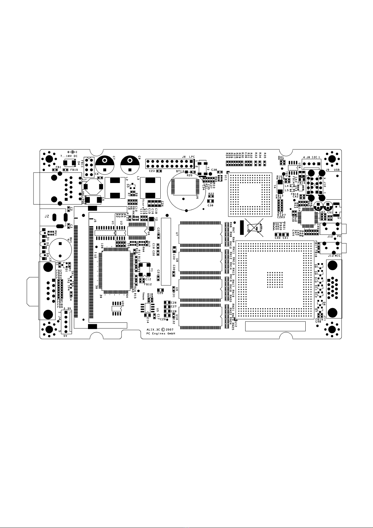
ALIX block diagram
Schematics wi be made avai ab e to qua ified customers.

ALIX system board 13 1/15/2008
ALIX connector pinouts
References refer to ALIX.2 / ALIX.3.
J5/J3 COM1 serial port
The standard PC pinout is used. To connect to a PC, use a nu modem or “Lap ink” cab e. Due to
imitations of the AMD CS5536 companion chip, handshake signa s are not avai ab e.
1 DCD data carrier detect (input) - not avai ab e on CS5536
2 RXD# receive data (input)
3 TXD# transmit data (output)
4 DTR data termina ready (output) - driven active
5 GND ground
6 DSR data set ready (input) - not avai ab e on CS5536
7 RTS ready to send (output) - driven active
8 CTS c ear to send (input) - not avai ab e on CS5536
9 RI ring indicator (input) - not avai ab e on CS5536
J12 / J4 COM1 serial port (build option)
As an option, the board can be configured with a 4 or 5 pin header with 3.3V CMOS signa eve s
instead of the norma RS-232 seria port.
1 V3 3.3V supp y
2 TXD transmit data (output)
3 RXD receive data (input)
4 GND ground
5 VCC 5V supp y
J3/J1 Et ernet port 1
RJ45 connectors with integrated magnetics are used. This port imp ements a passive power over
Ethernet scheme over the two unused pairs. Do not exceed 20V as the TVS protection diode may
start c amping above this vo tage.
1 TX+ transmit positive
2 TX- transmit negative
3 RX+ receive positive
4 VIN power supp y (nomina 7 to 20V)
5 VIN “
6 RX- receive negative
7 GND power return
8 GND “
J1, J2 / - Et ernet ports 2, 3
RJ45 connectors with integrated magnetics are used. These ports do NOT support power over
Ethernet. Same pinout as above, but pins 4,5 and 7,8 are not connected.

ALIX system board 14 1/15/2008
J6/J9 USB jack (build option)
Dua USB 2.0 connections:
1 VCC switched +5V supp y
2 DATA4- negative data
3 DATA4+ positive data
4 GND ground
5 VCC switched +5V supp y
6 DATA3- negative data
7 DATA3+ positive data
8 GND ground
J4/J2 DC power jack
This is a generic DC jack connector with a 2.1mm center pin. Recommended input vo tage is +18V.
center VIN Positive input vo tage
s eeve GND Ground
J7, J8 / J5, J14 miniPCI socket
These sockets imp ement the miniPCI interface. P ease see schematic for pinout.
J9 / - IDE eader (build option)
1 HDRST# IDE reset
2 GND ground
3 HDD7 IDE data 7
4 HDD8 IDE data 8
5 HDD6 IDE data 6
6 HDD9 IDE data 9
7 HDD5 IDE data 5
8 HDD10 IDE data 10
9 HDD4 IDE data 4
10 HDD11 IDE data 11
11 HDD3 IDE data 3
12 HDD12 IDE data 12
13 HDD2 IDE data 2
14 HDD13 IDE data 13
15 HDD1 IDE data 1
16 HDD14 IDE data 14
17 HDD0 IDE data 0
18 HDD15 IDE data 15
19 GND ground
20 key key pin (missing)
21 HDRQ IDE DMA request
22 GND ground
23 HDIOW# IDE I/O write
24 GND ground
25 HDIOR# IDE I/O read
26 GND ground
27 HDIORDY IDE I/O ready
28 CSEL cab e se ect (pu down)

ALIX system board 15 1/15/2008
29 HDACK# IDE DMA acknow edge
30 GND ground
31 HDIRQ IDE interrupt
32 nc no connect
33 HDA1 IDE address 1
34 HDPDIA# IDE diagnostic, 80 pin cab e ID
35 HDA0 IDE address 0
36 HDA2 IDE address 2
37 HDCS0# IDE chip se ect 0
38 HDCS1# IDE chip se ect 1
39 HDLED# IDE ed output
40 GND ground
41 VCC 5V power
42 VCC 5V power
43 GND ground
44 GND ground
J10 / J15 CompactFlas
The CompactF ash card is used in True IDE mode. Hot insertion is not supported – p ease power
off the unit before inserting a CF card.
1 GND ground
2 D3 IDE data
3 D4 IDE data
4 D5 IDE data
5 D6 IDE data
6 D7 IDE data
7 CS0# IDE decode (1F0..1F7)
8 A10 ground
9 ATASEL# ground to se ect true IDE mode
10 A9 ground
11 A8 ground
12 A7 ground
13 VCC +3.3V power supp y
14 A6 ground
15 A5 ground
16 A4 ground
17 A3 ground
18 A2 IDE address
19 A1 IDE address
20 A0 IDE address
21 D0 IDE data
22 D1 IDE data
23 D2 IDE data
24 IO16# 16 bit decode, not connected
25 CD2# card detect, not connected
26 CD1# card detect. not connected
27 D11 IDE data
28 D12 IDE data
29 D13 IDE data
30 D14 IDE data

ALIX system board 16 1/15/2008
31 D15 IDE data
32 CS1# IDE decode (3F6..3F7)
33 VS1# not connected
34 IOR# IDE read strobe
35 IOW# IDE write strobe
36 WE# connected to +3.3V
37 IRQ IDE interrupt
38 VCC +3.3V power supp y
39 CSEL# cab e se ect, ground = master
40 VS2# not connected
41 RESET# IDE reset, active ow
42 IORDY IDE ready
43 INPACK# IDE DMA request
44 REG# IDE DMA acknow edge
45 DASP# pu ed up
46 PDIAG# pu ed up
47 D8 IDE data
48 D9 IDE data
49 D10 IDE data
50 GND ground
The CompactF ash specification can be found at www.compactf ash.org.
J11 / J6 LPC expansion
The LPC port is used in the factory to connect an a ternate f ash BIOS to start the board when the
on-board f ash is corrupted or b ank. Use PC Engines adapter LPC.1A for this purpose if needed.
The LCP port can a so be used to connect a super I/O device. Un ike SC1100 based WRAP boards,
this port cannot be reprogrammed as GPIO pins.
1 LCLK0 LPC c ock (33 MHz)
2 GND ground
3 LAD0 LPC data 0
4 GND ground
5 LAD1 LPC data 1
6 GND ground
7 LAD2 LPC data 2
8 GND ground
9 LAD3 LPC data 3
10 GND ground
11 LFRAME# LPC frame
12 GND ground
13 PCIRST# reset (active ow)
14 CLK48 super I/O c ock (48 MHz)
15 ISP high to use LPC f ash, ow to use on-board f ash, pu ed ow by resistor
16 VCC +5V supp y
17 GND ground
18 V3 +3.3V supp y
19 SERIRQ seria interrupt
20 LDRQ# LPC DMA request

ALIX system board 17 1/15/2008
J13 / J8 I2C bus (build option)
This optiona header can be used to connect user specific hardware, e.g. a front pane
microcontro er, or for a icensing dong e. See AMD CS5536 data sheet for programming detai s.
1 +3.3V power supp y
2 SMB_SCL I2C c ock
3 SMB_SDA I2C data
4 GND ground
- / J12 Headp one out (build option)
- / J13 Microp one in (build option)
- / J11 VGA (build option)
1 VGAR VGA red
2 VGAG VGA green
3 VGAB VGA b ue
4 nc no connect
5 GND ground
6 GND ground
7 GND ground
8 GND ground
9 USBVCC +5V supp y (fused)
10 GND ground
11 nc no connect
12 DDCDAT DDC data
13 HS horizonta sync
14 VS vertica sync
15 DDCCLK DDC c ock
BT1 RTC battery (build option)
Footprint for CR2032 Lithium battery. P ease observe correct po arity, top side of the battery is +
positive termina . Specification: CR2032, horizonta mount, 20.4 mm ead spacing, for examp e:
Renata CR2032FH1
Panasonic BR2032-1HE
BU1 Buzzer (build option)
Optiona speaker. Driver circuit not popu ated, p ease contact PC Engines for instructions if you
wou d ike to add this.

ALIX system board 18 1/15/2008
Status LEDs
Status LEDs are a turned on by the BIOS on power up. The BIOS wi turn off LEDs 2 and 3
before booting the operating system.
Location GPIO read port write port
LED1 ( eft) G6 port 06100h bit 6 port 06100h bit 6 / 22
LED2 (midd e) G25 port 06180h bit 9 port 06180h bit 9 / 25
LED3 (right) G27 port 06180h bit 11 port 06180h bit 11 / 27
The CS5536 GPIO ports are programmed by 32 bit atomic writes. This avoids the need for read /
modify / write operations and the ocking issues they entai . For examp e, to turn off LED1 (high),
write 0000’0040h to port 06100h. To turn on LED1 ( ow), write 0040’0000h. Mu tip e port bits can
be changed at the same time.
Mode switc
The mode switch can be accessed by software as fo ows:
Location GPIO read port
MODESW# G24 port 061b0h bit 8 (active ow, 0 = switch pressed)

ALIX system board 19 1/15/2008
BIOS POST codes
tinyBIOS writes POST / diagnostic codes to port 80h. To make these codes visib e, use a miniPCI
POST card such as PC Engines POST.5A. POST codes are:
01 reset entry
02 chipset initia ization
03 detect base memory size
04 initia ize shadow RAM
05 init mono video
06 disab e PCI devices
07 test ow 64KB of DRAM
08 initia ize stack
09 BIOS checksum
0a super I/O initia ization
0b RTC test
0c refresh / 8254 test
0d speed-dependent chipset regs
0e test 8237 DMA
0f test DMA page registers
10 test 8254 registers
11 test keyboard contro er
12 init timer, DMA, 8259...
13 test 8259 mask registers
14 test ow 640KB
15 init vectors
16 PCI p ug & p ay
17 shadow video BIOS
18 ook for VGA BIOS
19 sign-on prompt
1a second keyboard test
1b extended memory test
1c enab e interrupts
1d test / init RTC
1e init f oppy disk
1f option ROM scan
20 test para e ports
21 test seria ports
22 enab e coprocessor
23 f oppy init
24 hard disk init
25 PS/2 mouse detect
26 timer/RTC check
27 OEM boot decision point
00 boot
33 NMI
F7 ow 64KB memory test fai ed
Other manuals for ALIX.2 Series
1
This manual suits for next models
1
Table of contents
Other PC Engines Motherboard manuals


