Philips SA58605 User manual

SA58605
Dual operational amplifier
and 2.5 V shunt regulator
Product data
Supersedes data of 2002 Mar 25 2003 Nov 12
INTEGRATED CIRCUITS

Philips Semiconductors Product data
SA58605Dual operational amplifier and 2.5 V shunt regulator
2
2003 Nov 12
DESCRIPTION
The SA58605 incorporates two op amps and 2.5 V shunt regulator
in an unique circuit configuration. The output of the device is
inverted when the inverting inputs of either or both op amps exceed
the internally set reference voltages at their non-inverting inputs.
Amp “A” is referenced to 2.5 V while Amp “B” is referenced to
154 mV. The SA58605 incorporates a “NOR logic” configuration with
these specific gate levels.
SA58605 supports voltage control and sensor applications such as
AC adapter, switch mode power supply and battery chargers. It is
available in a 5-lead small outline surface mount package
(SOP003).
FEATURES
•Low input bias current: 30 nA typ.
•Low operating supply current: 1.2 mA typ.
•Reference voltages at non-inverting inputs:
–Amp “A” at 2.5 V typ.
–Amp “B” at 154 mV
APPLICATIONS
•AC adapter and battery charger
•Switched Mode Power Supply (SMPS)
•Control voltage/sensor
SIMPLIFIED DEVICE DIAGRAM
AMP A
AMP B
4000 Ω
46920 Ω
3080 Ω
54
123
VCC AIN
BIN
GNDOUT
SL01618
Figure 1. Simplified system diagram.

Philips Semiconductors Product data
SA58605Dual operational amplifier and 2.5 V shunt regulator
2003 Nov 12 3
ORDERING INFORMATION
TYPE NUMBER
PACKAGE TEMPERATURE
TYPE
NUMBER
NAME DESCRIPTION VERSION RANGE
SA58605D SOT23-5,
SOT25, SO5 Plastic small outline package; 5 leads; body width 1.6 mm SOP003 –40 to +85 °C
Part number marking
The package is marked with a four letter code. The first three letters
designate the product. The fourth letter, represented by ‘x’, is a date
tracking code.
Part Number Marking
SA58605D AJAx
PIN CONFIGURATION
SL01613
1
2
34
5V
CC
AIN
BIN
GND
OUT
SA58605
Figure 2. Pin configuration.
PIN DESCRIPTION
PIN SYMBOL DESCRIPTION
1 OUT Output.
2 GND Ground.
3 BIN Amp B inverting input. Non-inverting input
internally set at 154 mV reference voltage.
4 AIN Amp A inverting input. Non-inverting input
internally set at 2.5 V reference voltage.
5 VCC Positive supply.
INTERNAL EQUIVALENT CIRCUIT
AMP A
AMP B
4000 Ω
46920 Ω
3080 Ω
54
123
VCC AIN
BIN
GNDOUT
SL01618
Figure 3. Internal equivalent circuit.

Philips Semiconductors Product data
SA58605Dual operational amplifier and 2.5 V shunt regulator
2003 Nov 12 4
MAXIMUM RATINGS
SYMBOL PARAMETER MIN. MAX. UNIT
VCC Supply voltage –0.3 +20 V
Tamb Ambient operating temperature –40 +85 °C
Tstg Storage temperature –40 +125 °C
PPower dissipation – 250 mW
ELECTRICAL CHARACTERISTICS
Tamb = 25 °C, VCC = 5 V (see Figure 6 “Test circuit”, and Table 1 “Parameter test circuit 1 and power supply settings”), unless otherwise
specified.
SYMBOL PARAMETER CONDITIONS MIN. TYP. MAX. UNIT
ICC Supply current AIN = 0 V; BIN = 0 V; RL= ∞– 1.2 1.7 mA
A amplifier
Vo(A) Output inverting voltage (A) BIN = 0 V; RL= 4.3 kΩ2.45 2.50 2.55 V
Ii(bias)(A) Input bias current (A) BIN = 0 V; RL= 4.3 kΩ– 30 150 nA
PSSR (A) PSSR (A) BIN = 0 V; RL= 4.3 kΩ62 – – dB
Io(sink)(A) Output sink current (A) AIN = 2.7 V; BIN = 0 V; VOUT = 1.5 V 5 – – mA
B amplifier
Vo(B) Output inverting voltage (B) AIN = 0 V; RL= 4.3 kΩ151 154 157 mV
Ii(bias)(B) Input bias current (B) AIN = 0 V; RL= 4.3 kΩ– 30 150 nA
PSSR (B) PSSR (B) AIN = 0 V; RL= 4.3 kΩ65 – – dB
Io(sink)(B) Output sink current (B) AIN = 0 V; BIN = 0.17 V; VOUT = 1.5 V 5 – – mA
TYPICAL PERFORMANCE CURVES
SL01615
VCC, SUPPLY VOLTAGE (V)
246
3.0
2.5
08
OUTPUT INVERTING VOLTAGE A (V)
10 12 14
2.0
1.5
1.0
0.5
0.0 18 20 2216 24 26 28 30
Figure 4. Output inverting voltage (A) versus VCC.
SL01616
VCC, SUPPLY VOLTAGE (V)
246
0.20
0.15
0.18
0.13
08
OUTPUT INVERTING VOLTAGE B (V)
10 12 14
0.10
0.08
0.05
0.03
0.00 18 20 2216 24 26 28 30
Figure 5. Output inverting voltage (B) versus VCC.

Philips Semiconductors Product data
SA58605Dual operational amplifier and 2.5 V shunt regulator
2003 Nov 12 5
TEST CIRCUITS
4000 Ω
46920 Ω
3080 Ω
2
3
4
5
1
AIN
BIN
OUT
GND
VCC
1 MΩ
S9
S4S3
1 MΩ
S8
100 kΩ
0.22 µF
0.1 µF
S12
1.5 V
VCC
OUT
RL
S11
S2S1
S7S6
1 kΩ
VIN
TPATPB
OFF
BIN
AIN
S5
47 µF
680 kΩ
1.5 kΩ
S10 0.22 µF
3.9 kΩ
1.5 V
SL01614
A
Figure 6. Test circuit.
Table 1. Parameter test circuit 1 switch and power supply settings
SYMBOL PARAMETER S1 S2 S3 S4 S5 S6 S7 S8 S9 S10 S11 S12 RL
(Ω)VIN (V) Comments
ICC Power supply current OFF OFF OFF OFF OFF OFF OFF ON ON OFF ON OFF 4.3 k
Vo(A) Output inverting voltage
(A) OFF ON OFF OFF AIN OFF OFF ON OFF ON ON OFF 4.3 k measure TPA
voltage
Ii(bias)(A) Input bias current (A) OFF OFF OFF OFF OFF OFF OFF ON ON OFF ON OFF 4.3 k measure TPA
voltage
Io(sink)(A) Output sink current (A) OFF OFF OFF OFF OFF OFF ON ON OFF OFF OFF ON 2.7 measure
output sink
current
PSSR (A) PSSR (A) OFF ON OFF ON OFF OFF ON ON OFF OFF ON OFF 4.3 k Vo(A) Note 1
Vo(B) Output inverting voltage
(B) ON OFF OFF OFF BIN OFF OFF OFF ON ON ON OFF 4.3 k measure TPB
voltage
Ii(bias)(B) Input bias current (B) OFF OFF OFF OFF OFF OFF OFF ON ON OFF ON OFF 4.3 k measure TPB
voltage
Io(sink)(B) Output sink current (B) OFF OFF OFF OFF OFF ON OFF OFF ON OFF OFF ON 0.17 measure
output sink
current
PSSR (B) PSSR (B) ON OFF ON OFF OFF ON OFF OFF ON OFF ON OFF 4.3 k Vo(B) –
20 mV Note 2
NOTES:
1. VOUT1 is defined by the voltage when VCC = 4 V. VOUT2 is defined by the voltage when VCC = 25 V. PSSR (A) is shown in Equation (1).
2. VOUT1 is defined by the voltage when VCC = 4 V. VOUT2 is defined by the voltage when VCC = 25 V. PSSR (B) is shown in Equation (1).
PSSR +40 )20logŤ(25 V *4 V)
(VOUT1 *VOUT2)ŤEquation (1)

Philips Semiconductors Product data
SA58605Dual operational amplifier and 2.5 V shunt regulator
2003 Nov 12 6
APPLICATION INFORMATION
The SA58605 may be used for various voltage control applications
in which the input threshold voltage exceed 2.5 V for Amp “A” and
154 mV for Amp “B”. When either or both input threshold voltage is
exceeded the output is pulled LOW. The output is connected to VCC
with a pull-up resistance.
Figure 7 shows the schematic for a Universal Converter/Charger
circuit in which the SA58605 Amp “A” is used to monitor the B+ level
of the converter/charger. Amp “B” input is pulled to ground through a
390 Ωresistor and will remain there. The input to the Amp “A” is
maintained at 0.5 ×B+ with the voltage divider of the two 1.5 kΩ
resistors. As B+ drops below 5 V, the input to Amp “A” of the
SA58605 follows and drops below 2.5 V. This causes the output
(pin 1) to go HIGH and the LED is turned off. Q1 base drive is
reduced and Q2 is increased. Thus, the PW modulation is
increased, and B+ is able to satisfy the load requirements of the
battery and circuitry. As B+ is increased above 5 V, it causes the
input to Amp “A” to increase above 2.5 V. Then, the output goes
LOW and the LED is activated which turns on the detection diode.
This increases the drive on Q1 and pulls down the base of Q2
reducing it base drive. With Q2 conducting less, the PW modulation
is decreased and B+ is reduced. Under quasi-steady state, B+ is
maintained at 5 V.
D1
D2
0.033 pF
8.2 kΩ
Q1
8.3 µF
/250 V
L1
10 mH Q2
2.7 kΩ
100 Ω
VIN = 85 – 265 VAC
0.1 µF
100 Ω
MUR160
56 kΩ
0.001 µF
/1 kV
D4
SA58605
5 4
1 32
390 Ω
Q4
Q3
100 µF
/16 V
800 µF
/8 V
1 MΩ
47 kΩ
D3
100Ω
0.1 µF
0.1 µF
0.22 Ω
390 Ω
1.5 kΩ
68 µH
1.5 kΩ
1 kΩ
100 µF
/16 V
B+
GND
SFH615A-4
SR01619
0.022 µF
T1
Figure 7. Universal converter/charger application.
Components used in Figure 7
D1–D4: 1N5822
Q1–Q4: 2N3904
T1: Cooper Electronic Technologies
Part#: CTX22-25348
Primary: 47 YTurns of #29 AWG, Pin 4 = Start, Pin 5 = Finish
Secondary: 5 Turns of 0.40 mm, Pins 1 and 2 = Start, Pins 7 and 8 = Finish
Gap: Designed for total primary inductance of 1.24 mH
Core: TSF-7070
Bobbin: Pins 3 and 6 removed, EE19

Philips Semiconductors Product data
SA58605Dual operational amplifier and 2.5 V shunt regulator
2003 Nov 12 7
PACKING METHOD
SL01305
TAPE DETAIL
COVER TAPE
CARRIER TAPE
REEL
ASSEMBLY
TAPE
GUARD
BAND
BARCODE
LABEL
BOX
Figure 8. Tape and reel packing method.

Philips Semiconductors Product data
SA58605Dual operational amplifier and 2.5 V shunt regulator
2003 Nov 12 8
Plastic small outline package; 5 leads; body width 1.6 mm SOP003

Philips Semiconductors Product data
SA58605Dual operational amplifier and 2.5 V shunt regulator
2003 Nov 12 9
REVISION HISTORY
Rev Date Description
_2 20031112 Product data (9397 750 12324). ECN 853-2334 30334 of 09 September 2003.
Supersedes data of 2002 Mar 25 (9397 750 09865).
Modifications:
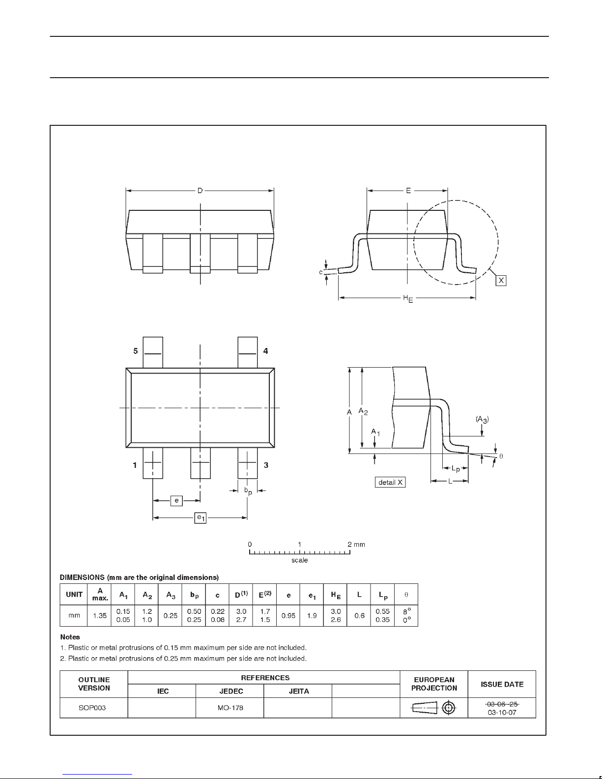
•Change package outline version to SOP003 in Ordering information table and Package outline sections.
_1 20020325 Product data (9397 750 09865). ECN 853-2334 27919 of 25 March 2002.
Definitions
Short-form specification— Thedatainashort-form specification is extractedfromafulldatasheetwiththesametypenumber and title. For detailed informationsee
the relevant data sheet or data handbook.
Limitingvaluesdefinition—LimitingvaluesgivenareinaccordancewiththeAbsoluteMaximumRatingSystem(IEC60134).Stressaboveoneormoreofthelimiting
values may cause permanent damage to the device. These are stress ratings only and operation of the device at these or at any other conditions above those given
in the Characteristics sections of the specification is not implied. Exposure to limiting values for extended periods may affect device reliability.
Application information — Applications that are described herein for any of these products are for illustrative purposes only. Philips Semiconductors make no
representationor warranty that such applications will be suitable for the specified use without further testing or modification.
Disclaimers
Life support — These products are not designed for use in life support appliances, devices, or systems where malfunction of these products can reasonably be
expected to result in personal injury. Philips Semiconductors customers using or selling these products for use in such applications do so at their own risk and agree
to fully indemnify Philips Semiconductors for any damages resulting from such application.
Rightto make changes —PhilipsSemiconductorsreserves therighttomakechangesintheproducts—includingcircuits,standardcells,and/orsoftware—described
orcontained herein in order toimprovedesignand/orperformance.Whentheproductisinfull production (status ‘Production’), relevant changes will becommunicated
viaaCustomerProduct/ProcessChangeNotification(CPCN).PhilipsSemiconductorsassumesnoresponsibilityorliabilityfortheuseofanyoftheseproducts,conveys
nolicenseortitleunderanypatent,copyright,ormaskworkrighttotheseproducts,andmakesnorepresentationsorwarrantiesthattheseproductsarefreefrompatent,
copyright, or mask work right infringement, unless otherwise specified.
Contact information
For additional information please visit
http://www.semiconductors.philips.com. Fax: +31 40 27 24825
For sales offices addresses send e-mail to:
sales.addresses@www.semiconductors.philips.com.
Koninklijke Philips Electronics N.V. 2003
All rights reserved. Printed in U.S.A.
Date of release: 11-03
Document order number: 9397 750 12324
Data sheet status[1]
Objective data
Preliminary data
Product data
Product
status[2] [3]
Development
Qualification
Production
Definitions
This data sheet contains data from the objective specification for product development.
Philips Semiconductors reserves the right to change the specification in any manner without notice.
This data sheet contains data from the preliminary specification. Supplementary data will be published
at a later date. Philips Semiconductors reserves the right to change the specification without notice, in
order to improve the design and supply the best possible product.
This data sheet contains data from the product specification. Philips Semiconductors reserves the
right to make changes at any time in order to improve the design, manufacturing and supply. Relevant
changes will be communicated via a Customer Product/Process Change Notification (CPCN).
Data sheet status
[1] Please consult the most recently issued data sheet before initiating or completing a design.
[2] The product status of the device(s) described in this data sheet may have changed since this data sheet was published. The latest information is available on the Internet at URL
http://www.semiconductors.philips.com.
[3] For data sheets describing multiple type numbers, the highest-level product status determines the data sheet status.
Level
I
II
III
Table of contents
Other Philips Amplifier manuals

Philips
Philips NE5512 Owner's manual

Philips
Philips TDA6107JF User manual

Philips
Philips TDA8928J User manual

Philips
Philips TDA4861 User manual

Philips
Philips TDA7053A User manual

Philips
Philips CMP400 User manual

Philips
Philips Plena Guide

Philips
Philips TDA4860 User manual

Philips
Philips BGY685AD User manual

Philips
Philips TDA6103Q User manual

Philips
Philips SBA3005/37 User manual

Philips
Philips FA 911 User manual

Philips
Philips car power amplifier User manual

Philips
Philips SDW5005 User manual

Philips
Philips SDW5005GN User manual

Philips
Philips SWV2116 User manual

Philips
Philips FA 911 User manual

Philips
Philips TDA2615 User manual

Philips
Philips BGY583 User manual

Philips
Philips TDA7057AQ User manual