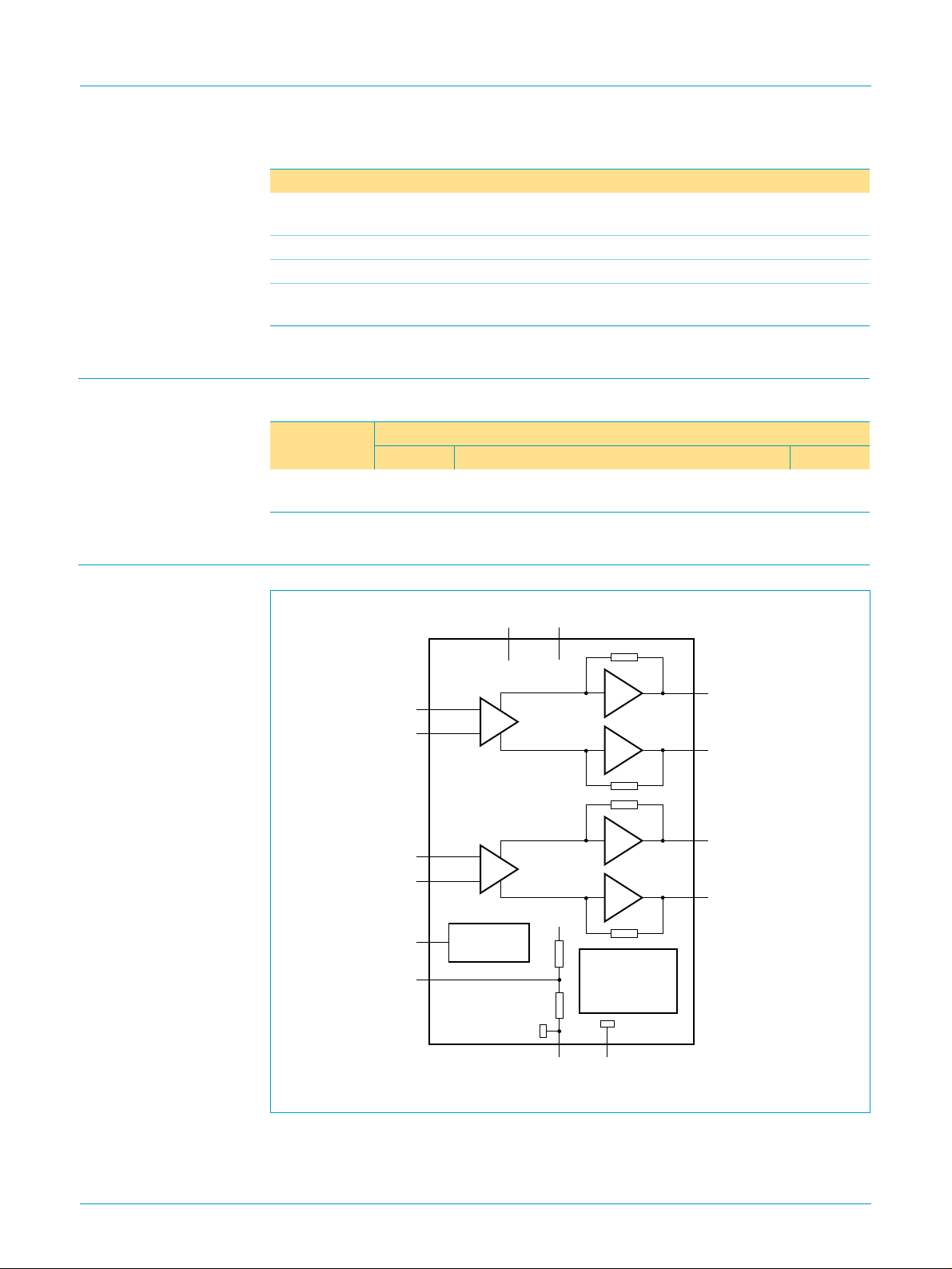
Philips Semiconductors TDA8946J
2 x 15 W stereo BTL audio amplifier
Product specification Rev. 02 — 14 March 2000 6 of 23
9397 750 06863 © Philips Electronics N.V. 2000. All rights reserved.
Mute — In this mode the amplifier is DC-biased but not operational (no audio output);
the DC level of the input and output pins remain on half the supply voltage. This
allows the input coupling and Supply Voltage Ripple Rejection (SVRR) capacitors to
be charged to avoid pop-noise. The device is in mute mode when
3V<V
MODE <(V
CC −1.5 V).
Operating — In this mode the amplifier is operating normally. The operating mode is
activated at VMODE < 0.5 V.
8.3.1 Switch-on and switch-off
To avoid audible plops during supply voltage switch-on or switch-off, the device is set
to standby mode before the supply voltage is applied (switch-on) or removed
(switch-off).
The switch-on and switch-off time can be influenced by an RC-circuit on the MODE
pin. Rapid on/off switching of the device or the MODE pin may cause ‘click- and
pop-noise’. This can be prevented by proper timing of the RC-circuit on the MODE
pin.
8.4 Supply Voltage Ripple Rejection (SVRR)
The SVRR is measured with an electrolytic capacitor of 10 µF on pin SVR at a
bandwidth of 10 Hz to 80 kHz. Figure 13 on page 12 illustrates the SVRR as function
of the frequency. A larger capacitor value on the SVR pin improves the ripple rejection
behaviour at the lower frequencies.
8.5 Built-in protection circuits
The TDA8946J contains two types of protection circuits, i.e. short-circuit and thermal
shutdown.
8.5.1 Short-circuit protection
Short-circuit to ground or supply line — This is detected by a so-called ‘missing
current’ detection circuit which measures the current in the positive supply line and
the current in the ground line. A difference between both currents larger than 0.7 A,
switches the power stage to standby mode (high impedance).
Short-circuit across the load — This is detected by an absolute-current
measurement. An absolute-current larger than 3 A, switches the power stage to
standby mode (high impedance).
8.5.2 Thermal shutdown protection
The junction temperature is measured by a temperature sensor; at a junction
temperature of approximately 150 °C this detection circuit switches the power stage
to standby mode (high impedance).