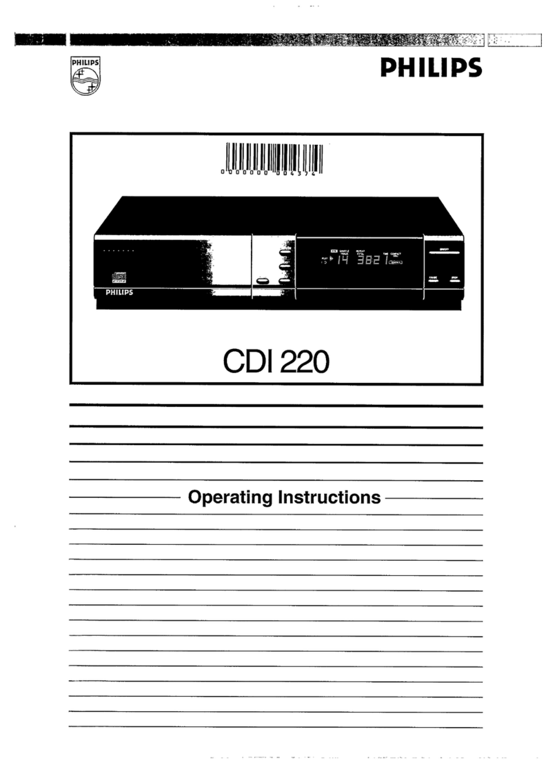
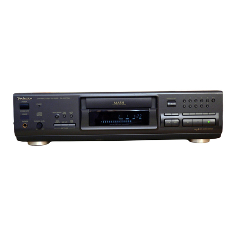
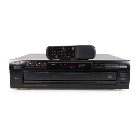
Philips CDI 220/00 User manual

Compact disc interactive player
~®[TWO©®
~®[TWO©®
Service
CONTENTS
illiiillllll~--
krlterac:thre
!'si1edi.a
Manual information
2 Product information
3 Service information
4 Mechanical drawings
and
partslist
5 Descriptions
6 Electrical drawings
and
partslist
7 Diagnostics, measurements and adjustments
Safety regulations require that the set
be
restored to its original
cond1t1on
and that parts which are
1dent1cal
with
those
spec1f1ed
be
used
·Pour
votre
securitl!,
ce.s
documents
.so111ent
etre
u1mses
par
des
spec1a-
li:s1es
a.gr~e5.
seul:s
habil11es
a
reparer
votre
appare11
eri
panna~
CDI
220/oo
CLASS
1
LASER
PRODUCT
31.2211003&20
Published by Service & Support Interactive Media Systems Printed in The Netherlands ©Copyright reserved Subject to modification 4822 725 24137
e PHILIPS

SECTION
CONTENTS
1
DETAILLED
TABLE
OF
CONTENTS
6
ELECTRICAL
DRAWINGS
6.1
WIRING
DIAGRAM
2
PRODUCT
INFORMATION
6.2 BLOCK
DIAGRAM
2.1
TECHNICAL
SPECIFICATION 6.2.1
Alphabetical
list
of
abbreviations
2.2
CONNECTIONS
AND
CONTROLS 6.3 POWER SUPPLY PANEL
1006
6.3.1 PCB
Lay-outs
3
SERVICE
INFORMATION
6.3.2
Circuit
diagram
3.1
SAFETY
INSTRUCTIONS
6.3.3
List
of
electrical
parts
3.2
SERVICING
OF
SMDs
(SURFACE
MOUNTED
6.4 CD PANEL
1004
DEVICES) 6.4.1
Circuit
diagram
CD
part
1
3.2.1
General
cautions
on
handling
and
storage
6.4.2
List
of
electrical
parts
3.2.2
Removal
of
SMDs
6.4.3 PCB
Lay-outs
3.2.2.1
Caution
on
removal
6.4.4.
Circuit
diagram
CD
part
2
3.2.3
Attachment
of
SMDs
6.4.5.
Circuit
diagram
turntablemotor
part
3.2.3.1
Caution
on
attachment
6.5
AUDIO
PROCESSING
UNIT
1002
3.3
HANDLING
ESD SENSETIVE
COMPONENTS
6.5.1
Circuit
diagram
3.3.1
Personal
safety
6.5.2 PCB
lay-outs
3.3.2
Storage
and
transport
6.5.3
List
of
electrical
parts
3.3.3
Testing
or
handling
6.6 VIDEO ENCODER
UNIT
1003
3.3.4
Mounting
ESD
sensetive
components
6.6.1 PCB
lay-outs
3.3.5
Soldering
6.6.2
List
of
electrical
parts
3.3.6
Electrostatic
charges
6.6.3
Circuit
diagram
3.3.7
Transients
(switch-on
phenomena)
6.7
MMC
PANEL 1001
3.3.8
Working
environment
6.7.1 PCB
lay-out
3.3.9
Replacement
of
the
Flat
Pack ICs 6.7.2 F.M.V.
interface
circuit
diagram
3.4
CODENUMBERS
FOR STANDARDIZED 6.8 DISPLAY
AND
HEADPHONE
PANEL 1005
RESISTORS 6.8.1 PCB
lay-out
3.5 SERVICE
TOOLS
6.8.2
List
of
electrical
parts
3.5.1
Service
PCB 6.8.3 PCB
layout
Headphone
panel
3.5.1.1
Circuit
diagram
6.8.4
Circuit
diagram
3.5.1.2
Layout
3.5.1.3
Parts
list
7
DIAGNOSTICS
3.5.2 Test
discs
7.1
TROUBLESHOOTING
AND
REPAIR
3.5.3
Extension
connectors
7.1.1
Troubleshooting
the
Power
Supply
3.5.4
Measurement
equipment
7.1.2
Troubleshooting
and
Service
the
MMC
panel
3.5.5
Pointing
devices
7.1.3
CO-part
and
Audio
Section
Troubleshooting
3.5.6
(de)Mounting
tool
7.1.4
Video
Section
Troubleshooting
3.6 THE
MMC
CENTRAL
REPAIR PROCEDURE 7.2
MEASUREMENTS
AND
ADJUSTMENTS
7.2.1
Power
supply
panel
1006
4
MECHANICAL
DRAWINGS
AND
PARTS
7.2.1.1
Checkspoints
LIST
7.2.1.2
Adjustment
4.1
DEMOUNTING
INSTRUCTIONS
OF
CABINET
7.2.2
CD
panel
1004
4.1.1 Top
Cover
Removal
7.2.2.1
Laser
current
4.1.2
Front
Assembly
Removal
7.2.2.2 Focus
signal
4.1.3
Display
Panel
Removal
7.2.2.3
Starting
signal
4.1.4
Power
Supply
Panel
Removal
7.2.2.4
Motor
control
signals
4.1.5
APU
panel
&
Encoder
Panel 7.2.2.5 Radial
error
circuit
signals
4.1.6
CDM
Loader
Assembly
Removal
7.2.2.6
Clock
signal
(LP
IC7201
4.1.7
CDM
Loader
Disassembly.
7.2.2.7
Decoder
signals
4.1.7.1 Tray
Removal.
7.2.2.8
Video
signals
4.1.7.2
CDM
Assembly
Removal
7.2.3
Audio
processing
unit
1002
4.1.8
Exploded
view
of
the
cabinet_
7.2.3.1
Slave
processor
data
4.1.8.1
Parts
list
of
cabinet
7.2.3.2 1
2S
signals
4.2 EXPLODED
VIEW
OF LOADER 7.2.3.3 X;n
clock
signal
4.2.1
Parts
list
of
LOADER 7.2.3.4 DEEMP
signal
7.2.3.5 FILTERN
signal
5
SERVICE
SOFTWARE
7.2.3.6 KIii
signal
5.1
THE
LOW
LEVEL
MMC
TEST 7.2.3.7
Performance
check
5.1.1
Tools
7.2.4
Video
encoder
unit
1003
5.1.2 Test
sequence
7.2.4.1
Check
and
adjustment
PAL
sub
carrier
5.1.3
Low
level
test
implementation
7.2.4.2
SW
control
signal
5.1.4
How
to
start
up
the
low
level
test
7.2.4.3
Check
of
RGB
input
signals
5.1.5 PCB
low
level
test
7.2.5
Multi
media
controller(
MMC
Panel) 1001
5.1.6
Terminal
low
level
test
7.2.5.1
Supply
voltages
5.1.7
Error
codes
7.2.5.2
Clock
signals
5.1.8
Release
number,
position
and
checksum
7.2.5.3
12S
interface
storage
7.2.5.4
Reset
circuitry
5.1.9
How
is
the
checksum
calculated
? 7.2.5.5
Main
(LP
68070
5.2 THE SERVICE SHELL 7.2.5.6
Low
Level
test
5.2.1
Starting
the
service
shell
5.2.2
Layout
info
5.2.3
Subject
dependent
information
PCS
66
312

2
PRODUCT
INFORMATION
2.1
TECHNICAL SPECIFICATION
Physical
Dimensions
(w
x h x
d)
420 x 90 x 400
mm
(16.5
x 3.5 x
15.
7 inch)
Weight
(approx.)
7
kg
(15.4 lbs)
Power supply
220/240 V ; 50-60Hz
220V range 198V
to
264V
Power consumption
Approx.
35W
Approvals
FCC,
UL
Conforms
with
VDE, FTZ, CSA,
Nordic,
US and GERMAN
laser
safety
regulations
Audio
L+R:
Connector
Type Cinch
connector
gold
plated 2x
Colour
Left:
white
Right red
Output
quality
in case
of
CD-DA
Measurements
acc.
to
IEC
TC
60 Subcan.
60A
Output
level :
2Vrms
+!-
3 dB
Frequency range : 20 HZ
to
20
kHz
Frequency
linearity
:
+0.2
dB/
-0.2
dB
Cross
talk
(1
kHz)
: - 86 dB
Harmonic
dist.
+ noise at 1
kHz
SIN
ratio
Dynamic
range
: -
86
dB
: 87 dB
(typ
>90)
: 86 dB
Output
quality
in case
of
ADPCM
to
be specified
Headphone output:
Connector
type
Output
control : Phone socket
:
Manual
volume
control
Output
quality
in case
of
CD-DA
Load
impedance
range
Output
power
Frequency range
Harmonic
distortion
(1
kHz)
S/N
ratio
Dynamic
range
Cross taIke Ri~600E
(1
kHz)
PCS 61848
: 8
Ohm
- 2 kOhm
: 30
mW
at 1
kHz,
32 Ohm
: 20
Hz
-20 kHz
+!-
3 dB
: - 83 dB
: 84
dB
: 83
dB
: - 75 dB
Video specifications
625 lines:
RGB
(PAL, SECAM)
for
/00/05
Connector
type
Pinning:
No. Function
:
Euroconnector
(SCART)
1.
Audio
R (analogue)
2.
NC
3.
Audio
L (analogue)
4.
Audio
ground
5.
Blue
ground
6.
NC
7.
Blue
8.
Slow
switching(
o~
TV,
1
~Euroconn.)
9.
Green
ground
10.
NC
11. Green
12.
NC
13. Red
ground
14.
NC
15. Red
16. Fast
switching
(RGB/CVBS)
17. CVBS
ground
18. Fast
switching
ground
19. CVBS/RGB sync
20.
NC
21
Shield
Video interface
General
information:
TABEL 1 Encoded
RGB
General
information
Resolution
normal
H*V
Line period
Active line
period
VSC
clock
Display
format
non-interlace
interlace
(2
different
frames)
interleaved
(2
identical frames)
PAL
Amplitude
Line time
Sync.
output
S/N
on
RGB
output
S/N
on
RGB
output
Bandwidth
on
RGB
out
CVBS output:
Connector
PAL
Amplitude
White
bar
Sync
amplitude
Burst
amplitude
S/N
lum. (40Hz-10MHz)
SIN
chrom. in red
Video
bandwidth
Chroma subc. freq.
: PAL
Environment
: 384*280
384*560
: 64.00 us
: 51.20 us
: 30.0000 MHz
: 312 lines
: 625 lines
: 625 lines
:
700mVpp
+!-
10%
(max.
white
level)
: 64.
us
: 300
mVpp
+!-
0.1V
into
75
Ohm
: >
50
dB (40
Hz
- 5 MHz)
: > 45 dB (40
Hz
- 10 MHz)
: - 3 dB at 7.5 MHz
: Cinch
connector,
colour
Yellow
:
1Vpp
+15%/-10%
: 700
mVpp
+110
mV/-70
mV
: 300
mVpp
+/-40
mV
: 300
mV
+l-30
mV
: fsc notch
>45dB
:
AM
(*) > 48 dB
PM
(**)
> 43 dB
: 4.5 MHz
(-6dB)
:
~
4.433661 MHz
X-tal locked
+!-50Hz
"
AM
noise :
output
of
measured value in dB referred
to
the average
amplitude
of
the
colour
subcar-
rier
burst
applied
**
PM
noise
:
output
of
measured value in dB referred
to
the
constant
phase
of
a reference
oscillator
V
/C
(S-Video) output:
Type
of
connector
Pinning:
No. Function
1. Gnd Y
2.
Gnd C
3. y
4. C
PAL
:
Mini-Din
4 (female)
amplitude
:
Y~
1Vpp
+15%/-10%
into
75
Ohm
amplitude
bandwidth
Y
bandwidth
C
S/N
on
Y
output
(10KHz-5MHz)
:c~ 300
mVpp
+!-
10% (burst)
:
~
5 MHz
(-3dB)
(10KHz-1 0MHz)
S/N
on
C
output
:
~
1.6 MHz
: > 48 dB
: > 45 dB
:
AM(*)>
55 dB
PM
(**)>
50
dB
*
AM
noise :
output
of
measured
value in dB referred
to
the average
amplitude
of
the
colour
subcar-
rier
burst
applied
**
PM
noise :
output
of
measured
value in dB referred
to
the
constant
phase
of
a reference
oscillator
Laser Detector Grating
Unit
(LDGU)
Laser
type
:
semi
conductor
AIGaAs
Wave length : 780
nm
Output
power
: 3.3
mW
typical
RS232-1 (port 1I communication:
Connector
type
: 8
pins
miniDIN (female)
Location
:
front
Internal device :
MMC
slave proc.
(68HC05,
SCl+ports)
Baudrates : 1200 and 9600
Dataformat
: 1
startbit
7
databits
2
stopbits
no
parity
Handshake :
hardware:
only
RTS
software:
not
available
Signals & Pinning:
pin signal
description
lnp/Outp
1 n.c.
Not
Connected
2 RXD Received Data
Input
3 TXD
Transmitted
Data
Output
4
DTR
(*) Data Terminal Ready
Output
5 GND Signal Ground
6 n.c.
Not
Connected
7
RTS
Request
To
Send
Output
8
+5V
Power
supply
for
the device
RS232-2
(port
2)
communication:
Connector
type
: 8 pins
miniDIN
(female)
Location : rear
Internal
device
:
on
chip UART (SCC68070)
Baudrates : 75, 150, 300, 1200, 2400,
Dataformat
stopbit
length
parity
Handshake
software
Signals & Pinning:
pin
signal
1 n.c.
2 RXD
3
TXD
4 DTR
(*)
5 GND
6 CTS
7 RTS
8
+5V
4800, 9600 and 19200
: character
length:
7
or
8 bits
: 1
or
2 bits
:
odd,
even
or
no
:
hardware:
2
control
lines;
RTS
and
CTS.
: XON/XOFF.
description
lnp/Outp
Not
Connected
Received Data
Input
Transmitted
Data
Output
Data Terminal Ready
Output
Signal Ground
Clear
To
send
Input
Request
To
Send
Output
Power
supply
for
the
device
Input
:
this
is an
input
signal
for
the CD-I
player
Output:
this is an
output
signal
for
the
CD-I player.
(*)
DTR
is
not
an active handshake signal. It serves
as
a
power
supply
for
some
input
devices.
All signal levels
and
current
ratings,
except
+5V
and
DTR
are
according
EIA RS-232-C standard.
RATINGS :
+5V
+/-10%
max.
200mA
DTR
:
+12V
+/-10%
max.
10mA
(Ri
~
1kQ)
IR
interface:
The
IR
(infra red) receiver
for
use
with
the
CD-I remote
control.
Specification
according
UAW-0422
characteristics
Data
format
Distance
Sampling
time
Receive angle
Infrared receiver
control
Device
Mains
socket:
Connector
:
RC-5
extended
format
infrared
transmission
data.
: 20 -800 cm.
:
~<
50
ms
: 45 degree
out
of
the
centre
line
:
GP1
U501 X SHARP
: 2-pol.
The
player
has
to
be Class I
equipment.
Modifications
without
notice

2.2 CONNECTIONS AND CONTROLS
Front
panel
control
functions
and
rear
connections
COi
front
panel
controls
1.
Disc
loading
tray
2.
Open/close
key
3.
"Previous"
key
for
instant
track
skip
4.
"Next"
key
for
instant
track
skip
5.
"Play"
key
6.
1/0
port
for
CD-I
pointing
devices
or
keyboard
7.
Headphone
socket
8.
Headphone
volume
control
9.
Pause
key
10.
Stop
key
11.
Power
"On/Off'
key
12.
Soft
tone
multifunction
dis
play
with
infra-red
remote
control
receiver
The
control
sits
conveniently
in
the
hand,
and
the
thumbstick
and
action
keys,
which
are
by
far
the
most-used
controls,
are
easily
operated
one-handed.
COi
rear
panel
connections
13.
Power
input
socket
14.
1/0
port
for
CD-I
pointing
devices,
keyboard
or
other
RS232
connection
15.
Antenna
in'
16.
Euroconnector
17.
Channel
selector'
18.
Antenna
our
19.
Y/C(S-video)output
20.
Audio
output
L
21.
CVBS
{video)
output
22.
Remote
control
in
23.
Audio
output
R
24.
Extension
socket
(for
22ER9141
Digital
Audio,Nideo
module)
•depending
on
version
22ER9051
Infra
red
remote
control
The
"Thumbstick"
remote
control
The
shape
and
layout
of
the
"Thumbstick"
control
were
the
subject
of
careful
ergonomic
studies
to
ensure
that
it
can
be
used
left-handed
or
right-handed,
in
big
or
small
hands.
1/3.
Action
keys
2.
Thumbstick
4.
"Play"
key
5.
"Pause"
key
6.
"Previous"
key
for
instant
track
skip
7.
Mute
or
TV
/COi
selector
key'
8.
Volume
control
down
key
9.
Volume
control
up
key
10.
"Next"
key
for
instant
track
skip
11.
"Stop"
key
'depending
on
version
The
user
shell
With
just
the
one
"point
and
click"
operation,
player
functions
can
be
controlled
so
easily
that
the
actions
become
intuitive.
This
is
because
of
the
player's
specially
designed
"user
shell"
program.
which
presents
a
series
of
screen
displays
that
not
only
allow
you
a
complete
choice
of
play
functions,
but
also
guide
you
in
selecting
them.
User
shell
screen
When
the
player
is
switched
on,
the
first
"user
she
I
I"
screen
invites
you
to
load
a
disc.
Playing
a
CD-I
disc
is
a
simple
matter
of
loading
the
disc
and
selecting
"Start"
on
the
"CO-I
start"
screen
which
then
automatically
appears.
The
CD-I
program
starts
to
run,
and
you
select
options
from
the
screen
according
to
choice.
For
CO-Digital
Audio
discs,
the
"user
shell"
presents
a
play
control
screen.
This
offers
more
than
just
the
functions
fitted
as
standard
on
CD
players
(and
also
provided
on
the
front
panel
and
remote
control).
It
offers
all
the
features
found
only
on
top-of-the-range
players.
These
include
Program,
Favorite
Track
Selection,
Title,
Shuffle,
Repeat,
Play
and
Scan.
Another
"user
shell"
screen
offers
"Personal
Preference"
settings.
These
include
date
and
time
display,
Scan
time.
Auto
Shuffle,
and
Repeat.
When
"Personal
Preference"
settings
have
been
made,
the
player
automatically
adopts
them
whe1
1
starting
up.
Further
"user
shell"
screens
provide
info1
mation.
CD-DA
programming
(FTS)
facil-
ities,
a
list
of
stored
programs
and
other
information.
and
control
for
CD
Graphics.
User
Shell
Functions
General
screens:
•
"Personal
Preference"
settings
screen:
Auto
Shuffle,
Auto
FTS,
Display
Time/Date,
Scan
Time,
Repeat
(Disc
or
Track).
•
Open/Close
(on
player
start-up
screen).
•
Info
screens
(depending
on
version
with
language
choice).
•
Memory
screen
(manages
CD-I
stored
data.
as
well
as
FTS
programs
and
titles).
•
Dim
Screen
(adjusts
screen
brightness).
Soft-tone
fluorescent
tube
display
(FTDI
The
multifunction
FTD
supplies
complete
and
continuously
up-dated
information
on
the
player
status.
1.
Disc
playing
2.
Track
3.
Minutes
and
seconds.
4.
Type
of
disc:
Compact
Disc
Interactive,
Compact
Disc
Digital
Audio,
Compact
Disc
Digital
Audio
with
Graphics
5.
Time
indicators:
show
that
the
time
displayed
is
Track
Time,
Total
Time,
Remaining
Track
Time,
or
Remain.
6.
Scan
active
7.
Repeat
active
CD-I
start-up
screen:
•
Start
CD-I
(starts
CD-I
application).
8.
Shuffle
active
or
Photo-CO
9.
FTS
active
10.
Mute·
11.
Pause
active
CD-Digital
Audio
screen:
12.
Remote
activity
indicator
•
While
Playing
:
Play,
Stop
and
Pause.
'depending
on
version
•
Play
Modes:
Scan,
Shuffle,
Repeat
and
FTS.
•
Control:
Fast
Forward,
Fast
Rewind,
Next
Track
(directly
selectable),
Previous
Track
(directly
selectable).
Program
(programming
of
selected
tracks
in
any
order),
Save
(stores
your
favorite
track
programme
and
allows
manual
input
of
titles
related
to
discs
or
FTS
programs).
Input
Port
Pin
Signal
Function
1/0
1
NC
Not
connected
z
RXD
Received
Data
I
3
TX
•
Transmitted
Data
0
4
DTR
Data
Terminal
Ready
0
5
GND
Signal
Ground
6
CTS
Clear
to
Send
I
7
ATS
Request
to
Send
D
8
+5V
Power
supply
to
device
AN
Connections
CVBS
output
lcinch)
Audio
output
12
x
cinch}
Remote
in
(cinch).
Antenna
input:
1
Vpp
into
75
Ohm
2
Vrms
into
75
Ohm
Z
Vpp
at
2.2
kOhm
75
Ohm'
RF
output:
75
Ohm'
Headphone
(6.3
mm
socket}
8
Ohm
Z
kOhm
V/C
IS-Video)
Connector
Pin
Function
1
Ground
Y
2
Ground
C
3 y
4 C
Euroconnector
•
Pin
Function
1
Audio
R
(analogue)
2
NC
3
4
5
6
Audio
L
(analogue)
Audio
ground
Blue
ground
NC
7
Blue
8
Slow
switching
(0
=
TV,
1=
Euroconnector)
9
Green
ground
10
NC
11
12
13
14
15
16
17
18
19
20
21
Green
NC
Red
ground
NC
Red
Fast
switching
(RGB/CVBS)
CVBS
ground
Fast
switching
ground
CVBS/RGB
sync
NC
Shield
'depending
on
version
PCS
66 313

3.1
SAFETY INSTRUCTIONS
-Safety regulations demand that the set be restored
to
its original condition and that
components
identical
with the original types be used.
Safety components are marked by the symbol A.
-
ESD
JA
~
All IC's and many
other
semi-conductors are
susceptible
to
electrostatic discharges (ESD).
Careless handling during repair can reduce life
drastically.
When repairing, make sure that you are connected
with the same potential as the
mass
of
the set via a
wrist wrap with resistance.
Keep components and tools also at this potential.
For detailed information see "Handling ESD-sensitive
components".
- A set to be repaired should always be connected to
the mains via a suitable isolating transformer.
-never replace any modules
or
any
other
parts while
the set
is
switched on.
-Use plastic instead
of
metal alignment tools. This
in
order
to
prelude short-circuit
or
to prevent a specific
circuit form being rendered unstable.
3.2 SERVICING OF SMDs (Surface Mounted Devices)
3.2.1 General cautions
on
handling and storage
a.
Oxidation on the
SMDs
terminals results in
poor
soldering. Do not handle SMDs with bare hand.
b.
Avoid for storage places that are sensitive to
oxidation such as places with
sulfur
or
chlorine gas,
direct sunlight, high temperatures
or
a high degree
of
humidity.
As a result the capacitance
or
resistance value
of
the
SMDs may be affected.
c.
Rough handling
of
circuit boards containing SMDs
may cause damage
to
the
components
as well as the
circuit boards. Circuit boards containing
SMDs
should
never be bent
or
flexed. Different circuit board
materials expand and contract
at
different rates when
heated
or
cooled and the
components
and/or
solder
connections may be damaged due to the stress.
Never rub or scrape chip
components
as this may
cause the value
of
the
component
to
change. Similary,
do not slide the circuit board
across
any surface.
3.2.2 Removal of SMDs
a.
Heat the solder (for 2-3 seconds)
at
each terminal
of
the chip. Small components can, by means
of
litz wire
and a limited horizontal force, be removed with the
soldering iron. They can also be removed with a
solder sucker (see Fig. 1
a)
or
b.
While holding the SMD with a pair
of
tweezers take it
off gently using th soldering
iron's
heat applied to
each terminal (see Fig. 1b).
c.
Remove the excess solder on the solder lands by
means
of
litz wire
or
a solder
sucker
(see Fig. 1
c).
3.2.2.1 Caution
on
removal:
a.
When handling the soldering iron, use suitable
pressure and be careful.
b.
When removing the chip,
do
not
use undue force with
the pair
of
tweezers.
c.
The soldering iron to be used (approx. 30
W),
must
preferably
be
provided with a thermal control
(soldering temperature about 225
to
250°C).
d The chip, once removed,
must
never be used again.
PCS 61850
DlSMOIJNTING
HEATING
>,l
OR
A
a
HEATING
',.,
SOLrJf.RlNG
moN
\ \
SOil..DER
WlCKa;.t-n..
"~\
CLEANING
µ C
Fig. 1
3.2.3 Attachment of SMDs
43
161
A.11
a.
Locate the SMD on the
solder
lands by means
of
tweezers and
solder
the
component
at one side.
Ensure
that
the
component
is positioned well on the
solder lands (see Fig. 2a).
b.
Next complete te soldering
of
the terminals
of
the
component (see Fig. 2b).
MOUl'ITII\IG
Fig. 2
"t.,_OfRlt•H3
,,.,.,..!RON
3.2.3.1 Caution
on
attachment:
Fig. 3
a.
When soldering the SMD terminals,
do
not
touch them
directly with the soldering iron. The soldering
must
be
as quick as possible; care
must
be taken
to
avoid
damage to the terminals and the body itself.
b. Keep the
SMD's
body in
contact
with the printed
board when soldering.
c.
The soldering iron
to
be used (approx. 30
W)
must
preferably be provided
with
a thermal
control
(soldering temperature
about
225 to 250°C).
d. Soldering should
not
be
done
outside the solder land.
e. Soldering flux (of rosin) may be used but should
not
be acidic.
f. After soldering, let the SMD cool
down
gradually at
room temperature.
g. The quantity
of
solder
must
be proportional with the
size
of
the solder land. If the quantity is
too
great, the
SMD might crack
or
the
solder
lands might be torn
loose from the printed board (see Fig. 3).
TOOLS
TO
BE
USED
ANTISTATIC
MAT
MAGNIFYING
GLASS
CUTTING
THE
LEADS
HAIR ORYER
-------•···•··•"--
METAL
BRUSH
DISMOUNTING
CLEANING
THE
TRACKS
WRONG
TRACKSWlLL
BE
DA.MAGED
ALIGNING THE LEADS
RIGHT WRONG WRONG
4822 390 50025 W
~FLUX
BRUSH ' ,,,,;, 4822
321
40042
OESOLDEA BRAIO
SOLDERING
IRON
WELLER TCP
50
00,S-0,8 MM
FIXING
IC
AT
THE CORNERS
RIGHT
MOUNTING
DRYING
SOLDER TIP
WELLER PT-CC7
4822 310 50081
,,
"''""'
:::
KNIFE
APPLYING
FLUX
SOLDERING
WRONG WRONG

3.3 HANDLING ESD-SENSITIVE COMPONENTS
3.3.1 Personal safety
The testing, handling and replacing
of
ESD-sensitve
components requires special attention
for
personal
safety. A person dealing with ESD-sensitive
components should, normally speaking. be connected
via a resistance to the same potential as the chassis
of
the set to protect him against direct contact with
the supply voltage.
This resistance is often applied
in
the connection lead
of
wrist wraps. If necessary, make use
of
an isolating
transformer.
3.3.2 Storage and transport
Transport and store the circuits and PCBs
in
their
original packages.
As
an
alternative to the original package one may use
a conductive material
or
special
IC
package which
short-circuits all the pins
of
the
component
with one
another. ·
Always discharge the package before opening
it
3.3.3 Testing or handling
Work on a conductive surface when testing loose
circuits and components
or
when transferring
components and circuits from one package
to
another.
Use a conductive
wrist
wrap
with lead
to
make an
electrical connection between the conductive surface
and yourself via a resistance
in
the connection lead
of
the wrist wrap.
Connect equipment and tools also with this conductive
surface.
Do not connect any signals to inputs as long
as
the
power supply
of
the set to be tested is off.
All the inputs that are not used should
be
connected
either to ground or to the supply voltage. When
testing, do not use any freon sprays
for
under-cooling
of
sensitive components.
3.3.4 Mounting ESD-sensitive components
Mount ESD-sensitive components only
after
all
other
components have been mounted.
Make sure that the components themselves, the metal
parts
of
the PCB, mounting equipment and mounting
operator are at the same potential level as the chassis
of the set.
If it is impossible to ground the PCB, the mounting
operator should pick the PCB up before bringing it
into contact with the components
to
be replaced.
Conductive sheet
Soldering iron
Bit
3.3.5 Soldering
Soldering iron tips, also
those
of
low-voltage soldering
stations, should be
kept
at
the same potential
as
the
components
and the PCB.
It is
better
to
use solder-removing braid than solder
suckers.
3.3.6 Electrostatic charges
One should stick to the precautionary measures also
after the ESD-sensitive
components
have been
mounted on the PCB. Until the sub-PCBs have been
incorporated into a complete system on which the
correct
supply voltages are connected, the PCB is
nothing more than an extension
of
the
conductors
of
the
components
on this PCB. To prevent electrostatic
discharges from passing to the
components
via the
terminals, we recommend
that
you apply conductive
clips
or
conductive tape on the terminals
of
the PCB.
3.3.7 Transients (switch-on phenomena)
To prevent permanent
damages
as a
result
of
switch-on phenomena, no ESD-sensitive components,
or
PCBs populated with these components, should be
inserted
in
or
removed
from
test-sockets
or
systems
with the supply voltage on.
Prevent switching
peeks
on the mains as a
consequence
of
switching electric equipment, relay
and DC lines on and off.
3.3.8 Working environment
The
work
bench
for
the service technician should look
like the one shown
in
the figure.
3.3.9 Replacement of the Flat Pack IC's
For replacing a
component
see Fig. 6 Dismounting
and Mounting. Also a
number
of
precautions and
examples is given.
When replacing a flat pack, rosin flux applied to the
device leads will ensure a
good
soldered joint.
Since rosin flux, when
not
properly heated by the
soldering process, is sticky, it will attract
dust
which
will result
in
component
degeneration
over
a period
of
time.
The removal
of
excess flux with a cleaner will not
solve this problem because the flux
is
then even
spread
over
a greater area by the cleaner. Drying
of
the flux can be accomplished by blowing the area with
a
common
hair dryer
for
1
or
2 minutes
at
a distance'
of
approx. 1
O
centimeters.
I•
Safety isolating transformer
Plug/socket
Wrist wrap
Special attention should be paid
in
regions having a
dry atmosphere and when the floor is covered with a
nylon carpet or such.
3.4 CODENUMBERS FOR STANDARDIZED RESISTORS
Unless otherwise specified, all defective resistors
in
the
circuits
of
the set can be replaced
by
standardizes types,
mentioned
in
this chapter.
VR25, VR37 high-ohmic/high -voltage resistors
type
Dmax
L1
max
L2
max
d
VR25 2.5 6.5 7,5 0,6
type
Dmax:
Li
max
L2max
d
VR37 I 3.7 I
9.0
100
I 0.7
Range VR25 : 100
KQ
to
22
MQ
Range VR37 : 100 KQ
to
33
MQ
Composition of the service number
for
the VR25 and VR37
Main subgroup: 4822 053 20
...
and 4822 053
21
...
The codenumber above is completed by inserting the
first two figures (resistance code) followed by the
multipHer.
4 for R = 100K to 910
Kn
5forR=
1M
to9.1
MQ
6 for R =or > 10M
Example's:
The serv.nbr. for a VR25 resistor
of
100
Kn
is
4822 053 20104
The serv.nbr. for a VR37 resistor
of
33
MQ
is 4822 053 21336
PR01, PR02 and PR03 power metal film resistors
itiDmaK
L1
L2ma:a.
-,,d
2.5 6.5 8,0 0.6
K I
L2-
fl •
¢-Dm.ax
L1
max
L2max
-¢d
3.9 10
11
0.8
tJ!Dmax
L
lmax
L2m.ax ¢
5.2 16.7 17.9 0,8
1•-u7
l
==~1~
7:JE)::::t==l==
~L2-l
01
0
t0d
Rated dissipation at T(amb) = 70 degrees :
PR01
= 1 Watt, PR02 = 2 Watt, PR03 = 3Watt
Composition of the service number
for
the PR01, PR02
and PR03
Main subgroup: 4822 053 10
...
; 4822 053
11
...
and 4822
053 12
...
The codenumber above is completed by inserting the
first
two
figures (resistance code)followed
by
the
multiplier.
8
for
R= 1 to 9,1 n
9
for
R= 10 to
91
n
1forR=
100
to910n
2 for R= 1
to
9,1
KU
3
for
R= 10 to
91
KU
4
for
R= 100 to 910
Kn
5
for
R=
or
> 1
Mn
Example:
The serv.nbr.
of
a
PR01
resistor
of
47 U
is: 4822 053 10479
The serv.nbr.
of
a PR03 resistor
of
1
Mn
is: 4822 053 12105
NFR25 fusible resistors A
L-
Ln,a,x
2.5
6.s
I
o.6
..;1
00
Composition
of
the service number
for
the NFR25
Main subgroup: 4822 052 10
...
The codenumber above is completed by inserting the
first
two
figures (resistance code)followed by the
multiplier.
8
for
R=
9
for
R=
1
for
R=
2
for
R=
3
tor
R=
Example:
1
to9,1
u
10
to91
u
100 to 910 n
1
to9,1Kn
10to91Kn
The service number
of
a resistor
of
47 U
is: 4822 052 10479
NFR25H fusible resistors A
2,5 6,5 0,6
..;
1
Composition of the service number
tor
the NFR25H
Main subgroup: 4822 052
11
...
The codenumber above is completed by inserting the
first
two
figures (resistance code)followed by the
multiplier.
8 for
R=
9 for
R=
1 for R=
2 for R=
3 for R=
Example:
1
to
9,1
n
10
to
91
u
100
to910n
1
to9,1Kn
10
to
91
Kn
The service number
of
a resistor
of
47 n
is:
4822 052 11479
RC-01, RC-11 AND
RC-21
chip resistors
I
1.25
.±.
0.15
>-----
3.2~~-.~~------
All
dimensions
in
mm
I
>-----
20!.015
-~-1
/
>-----
L6±o.,o--~
Absolute max. dissipation :
protect1;,e
c-o.i,t
A•)=
0.25:!0.15forstyle1
or
0.40
:!:
0.20 for style 2
RC-01
: 0,25
W,
RC-11 : 0,10
W,
RC-21 :0,062
W.
Range:
RC-01
0 Q TO 10 MQ
RC-11
0 Q TO 10 MQ
RC-21
0 Q TO 6,8 MQ
Composition
of
the service number
for
the RC-01,RC-11
and RC-21
Main subgroup: 4822
051
10
...
, 4822
051
20
..
and
4822
051
30
...
The codenumber above is completed by inserting the
first
two
figures (resistance code) followed by the
multiplier.
8 for
R=
9 for
R=
1 for
R=
2 for
R=
3 for
R=
4 for
R=
5 for
R=
6 for
R=
or>
Example's:
o
to9.1
n
10 to
91
n
1
oo
to
91
on
1
to9.1
Kn
10 to
91
Kn
100 to 910
KQ
1
to9.1
MQ
10
Mn
The serv.nbr. for a
RC-01
resistor
of
on
is
4822
051
10008
The serv.nbr. for a RC-11 resistor of
on
is
4822
051
20008
The serv.nbr. for a RC-21 resistor
of
o n is 4822
051
30008
The serv.nbr. for a RC-01 resistor
of
10 n is 4822
051
101
09
The serv.nbr. for a RC-11 resistor
of
10 n is 4822
051
20109
The serv.nbr. for a RC-21 resistor
of
10 n is 4822
051
30109
MRS16T metal film resistors with low-inductance
.~u-1
~Od
D
'
'~L2-
0D
L2
ma,:,;.
3,7
0,5
-0,04
Composition of the service number for the MRS16T
Main subgroup: 4822 050 1....
The codenumber above
is
completed by inserting the
first three figures (resistance code)followed by the
multiplier.
8 for R= 4,99 to 9,76 n
9 for
R=
10 to 97,6 u
1 for
R=
100 to 976 u
2 for R= 1 to 9,76 KQ
3 for R= 10 to 97,6
Kn
4 for R= 100 to 976
Kn
5 for R=
or>
1
Mn
Example:
The service number of a resistor
of
487 n is:
4822 050 14871
MRS25 metal film resistors (0,5%)
D
L1
L2
max
2.5
6.5 7,0 0.6 ± 0,03
Composition
of
the service number for the MRS25
Main subgroup: 4822 050 2....
The codenumber above is completed by inserting the
first three figures (resistance code)followed by the
multiplier.
8
for
R= 1 to 9,76 n
9 for R= 10 to 97,6 n
1 for R= 100 to 976 n
2 for R= 1 to 9,76 Kn.
3 for R= 10 to 97,6
Kn
4 for R= 100 to 976
Kn
5 for R= 1 to 9,76
Mn
6 for
R=
or
> 1o
Mn
Example:
The service number of a resistor of 976 n is:
4822 050 29761
PCS 61851

3.5 SERVICE TOOLS
3.5.1 Service
PCB
3.5.1.1
Circuit diagram
!ii!
~
l
1002
H
l
1201
E
5
l!ll
:l
JOll
G
2
3014
H 2
im
ii 1m[i
3011
D8 6
00
4
G
6
6001
E
1
60
01
F
1
6
00
8 E l Sl
1000
D 4 Sl
1001
I 2 Sl
100
2 I 6 Sl
U !l
G 8 Sl
F
8
Sl
n
D
8
C
8
,-------------------------1
+s
v
1
PCS
61852
SERVICE
PCB
CIRCUIT
DIAGRAM
2002
2001
,t.
I
56n
I
33u
/
16V
I
~
~-
___
__
+_sv_ 8 Sl
+SV
+5
V
~
"'~
0
~
~~
RESET
IRQ
2006
)
lu/16V I NC
VPP
11
PAO
6008
PA
!
BZX55C
4
V9
PA2
PA)
PA4
+5V
PA5
PA6
PAJ
TE
ST
~
"'
.r-<:
~
oo
PBO
+5V
PB!
PB2
"'
YES
~
PBS
.r-<:
~
01
PB6
+
SV
PBJ
"'
NO
~
.r-<:
~
02
NC NC NC
MSH
l~~lA
D!Sl
8 9
10
+SV
7000
40
680
5
C4
VDD
DSC!
OSC2
P
Dl
TOO
/
PD6
SS
/
PD5
SCK
/
PD4
i,()SJ
/ P
D)
HI
SO
/
PD2
TOO
/
PD
!
ROI
/
PD
O
PCO
PC!
PC2
PC)
PC
4
PCS
PC6
PC
J
VS
S
TCAP
20
NC
NC
11
12
BBBB
l 2 3
4
6
J
+SV
+SV
DEi
CLK
DAT
A.
39
38
36
35
NC
2003
34 NC
41p
I
JJ
NC
32
NC
JI
NC
JO
NC
29
)J
NC
+5V
"'
~
CERA.~
.
RESON
A
TO
R
+5V
+sv
+5V
+
SV
~!:!
~
~
"'
0
~~
NC
NC
Nc
8
J
0
jj
02
A
om
B
910
t
5V
NC NC
11
12
BBBB
l 2 l 4 6 7
+sv
+sv
D
E2
CLK
D
ATA
I
RTS
IJ Sl
+5V
I
·U
..
,
J-
5S
1
NC
~
4 Sl
I
RXD
2S1
TXD
l
Sl
I
NC L
l Sl
L
_________________________
_l
3.5.1
.2 Layout
3.5.1.3 Parts list
ITEM
1000
1001
1002
1201
2001
2002
2003
2004
2005
2006
3001
3002
3003
3004
3005
3006
3007
3008
3009
G4
LJ
G3
OBb
D004 I
coos
I
ROOS
I
I D007
~
'" I R001 I
I
R006
I
rn
n
;,
l
D001
11
ROOS
I
10
01
~
~
1002
c:,
c:,
a:
a:
L... L...
I
R012
I
~~
~
~
g
I
ROH
I
I
.JDDi
ii
R007 I I
R009
I
-,
co
04
c::::::::J
I R010 I
I
R003
I
CE:SCJ
201
I~
~~~l
1000
B b
D008
I
iswoo
I
~~~
lswo2 1
l
swo
1
I
YES
TEST
NO
G1
G2
DE
SC
RIPTION CODENUMBER ITEM DESCRIPTION CODENUMBER
Tact
switch
4822 276 10974 3010 22
KQ
Tact
switch
4822 276 10974
3011
22
KQ
Tact
switch
4822 276 10974 3012 22
KQ
3013 22
KQ
Ceram.
resonator
4822 242 72527 3014 22
KQ
3015 22
KQ
33
IF
/16V 4822 124 20688 3016 22
KQ
56 nF 4822
121
41154 3017 100 Q
47
pF 4822
122
31072
47
pF 4822
122
31072
6001
1N4148 4822 130 30621
100 IF/25V 4822 124 20701 6002 BC558B 4822
130
44197
1
IF
/63V 4822 124 20722 6003 BC548B 4822
130
40937
6004 1N1448 4822 130 30621
4,7 Q See standardized
list
6005
BZX55
C4V7 4822 130 34174
22
KQ
chapter
3.4 6006 BAT85 4822 130 31983
220
KQ
6007 1N1448 4822
130
30621
10
KQ
100 Q 7000 MC68HC705C4 4822 900 10272
22
KQ
7001
MSM
4202A
4822
130
90474
4,7
KQ
7002
MSM
4202A
4822
130
90474
10
KQ
22
KQ
S1
miniDIN
Spins 4822 267 31289

3.5.2 Test discs
CODE-
NUMBER
4822 397 30096
4822 397 30155
4822 397 30184
4822
701
11922
4822
701
11923
NAME/
DESCRIPTION
Testdisc 5
(music)
Testdisc 5A
(music+
dropouts
and fingerprints)
test disc
with
1
KHz
continous
signal, 70 minutes.
Audio
signals
Skew
disc 0,6
Excentricity disc
150
I
3.5.3 Extension connectors
CODE-
NUMBER
NAME/
DESCRIPTION
4822
321
22267
10
poles ext.
4822
321
22268 6 poles ext.
3.5.4 Measurement equipment
Electronic Digital
Multimeter
Digital oscilloscope
Analog oscilloscope
Timer/counter
3.5.5 Pointing devices
CODE-
NUMBER
NAME/
DESCRIPTION
4822
218
10401
RV6701
/00
4822
218
10438 RV6703/00
4822
691
30244
22EA9011
/00
3.5.6
(de)Mounting
tool
APPLICATION
Reference disc
for
playability and
adjustments
of
CDM
life test in case
of
intermittent
faults
Measure specs.
Reference disc
for
playability
Reference disc
for
playability
APPLICATION
For measuring
Encoder panel
For measuring
APU panel
APPLICATION
Remotecntrl.
/05
Remotecntrl. /00
Mouse
Torx
screw
drivers 4822 395
50145
3.6 THE
MMC
CENTRAL
REPAIR
PROCEDURE
In
case
of
a
defect
on the
MMC
part, the complete panel
must
be sent back
to
PCS
for
repair.
Below
a
brief
description is given, a more detailed proce-
dure is available at
P.C.S
Logistics Management, systems
and Procedure Office.
CODENUMBER
MMC:
Version
/00,/05
/11
/17P
/17T
Codenumber
4822
214
51981
4822
214
51979
4822
214
51933
4822
214
51938
NSO
or
Customer: send telex
or
on-line MSH system
info to
PCS
customer
relations
officer
with
indicated
number(s) and service
12NC
for
a repair reference num-
ber.
PCS:
send telex or MSH
info
with
repair reference num-
ber and return invoice price. Also the same number(s)
of
new/repaired
items are sent
with
invoice.
NSO or customer: send defective item(s)
to
PCS
at
SDM1
by
standard address label
with
repair reference
number
and return invoice
to
PCS
-price center.
Remark: the difference
between
the invoice price and
return invoice price gives the 'repair price'
for
the NSO
PCS:
send defective item
to
factory
and stock.
Experience has learned
that
the status
of
the particular
products and packaging needs
your
local attention.
Products
will
be returned in case
of
unacceptable condi-
tions.
REPAIR
PROCEDURE CONDITIONS :
HANDLE WITH
CARE
IN
AN
ESD
PROTETECTED
ENVIRONMENT.
Defective
items
must
be sent back
to
PHILPS
CON-
SUMER
SERVICE
for
repair
forwarded
by
Address
sticker.
Put the address sticker
properly
on a free area
of
the
box.
Boards
must
not
be reworked
or
damaged.
Re-use original package
order
new
package in case
of
damages.
Remove additional stickers and labeling
if
re-using the
original box.
Service
codenumber
on sticker
must
be equal to code-
number
on
repairable item.
!!!
If
the above conditions are
not
fulfilled, hen boards
are not accepted and the return price
will
not
be
credited !!!

4
MECHANICAL
DRAWINGS
AND
PARTS
LIST
4.1
DEMOUNTING
INSTRUCTIONS
OF CABINET
NOTE:
Numbers
in
parenthesis()
refer to the
Exploded
View
reference
numbers.
4.1.1
Top Cover Removal {216}
Remove the
four
Top Cover
screws
on
both
sides
of
the
LIil
it.
4.1.2 Front Assembly Removal (202}
Remove the Top Cover, refer
to
section
4.1.1.
Remove the COM Tray Front
assembly
(203) by
opening
the COM
Drawer
anci
lifting
the CDM Tray
Front
Assembly
up. Remove the three
front
screws
on
the
top
of
the
Front
Assembly
anci
the three
front
screws
on the
bottom
of
the
front
assembly. Remove the
two
top
front
frame
corner
screws
located
directly
behind
the
FrontAssembly
tpo
corner
screws.
Note:
By removing
the
two
top
front
frame
corner
screws,
the
two
bottom
Front
assembly
clips
will
disen-
gage from
the
bottom
of
the
Front Frame Bracket (502}
Carefully angle the the
top
of
the Front
Assembly
and
slide
the Front
Assembly
Cover
off
of
the unit.
Remove
the
two
screws
of
the the
HP
Panel (1007)
mounting
bracket. Dis-
connect
the
two
connectors
on the Display panel (1005).
Note:
Connectors are removed from
connector
sockets
by
releasing
the
socket
connector
clips.
Remove the Power
Switch
Connector
Shaft
(522) by
pulling
it
forward
out
of
Front Frame Bracket (502).
4.1.3 Display Panel Removal (1005}
Remove the Top Cover, refer
to
section
4.1.1.
Remove the Front
Assembly,
refer
to
section
4.1.2.
Remove the seven
screws
attaching
the
Display
Panel
to
tile
Front
Assembly
(202)
4.1.4 Power
Supply
Panel Removal (1006)
Remove the Top Cover, refer
to
section
4.1.1.
Remove the Rear Textplate (513)
by
removing
the
four
screws. Remove the
two
Power
Supply
mounting
screws
on the Rear Frame Bracket (514).
Remove the
two
Power
Supply
mounting
screws
on the
Riyht
Frame Bracket
(518).
Note.
The
two
Power
Supply
screws secured
to
the
Right Frame Bracket
ate
mounted
to
a heatsink on
the
Power
Supply
Panel. Be careful!
not
to
damage
the
Power Supply Panel
when
disassembling
&r
assembling.
Remove the Power
Supply
mounting
screw
located
on
the
top
front
of
the Power
Supply
Brncket (517).
Remove
the
power
switch
connecting
cable
from
the Cord
Clamps
(504,
508).
Lift
the
front
of
the
Power
Supply
Panel
up
two
inches
and
remove
the
two
connectors.
Slide
the
power
Supply
Panel
out
toward
the
front
of
the unit.
Disconnect
the
remaining
connector.
4.1.5 APU panel & Encoder Panel (1002, 1003).
Remove the Top Cover, refer
to
section
4.1.1.
Note:
The
APU Panel and Encoder Panel are
attached
to
the
CD Panel (1004)
by
two
PCB connectors for each
Panel. Both panels are also secured
in
place
by
guides
that
protude from
both
the
Left
Frame Bracket (506).
Remove all
wire
connectors
attached
to
the Panels and
carefully
lift each panel
up
out
of
the
PCB
connectors.
4.1.6 COM Loader Assembly Removal (212)
Note:
The
laser diode
is
extremely
sensitive
to
static
electricity.
Before Removing the COM Loader Assembly, properly
ground yourself using a
Wrist
Grounding Strap.
Remove the Top Cover,
refe1
to
section
4.ll
Remove the Front
Assembly,
refer
to
section 4.1.2.
Oµen the CDM
Drawer
and
rernove the
two
front
mounting
screws.
Remove
the
rear
mounting
screw. Lift the
front
of
the CDM
Loader
Assembly
one inch
and
locate the CDM
flat
cable and
flat
cable
socket.
Lift
the
top
of
the
socket
to
release the cable, pull the cable
up
from
the
connector
and
immediately
attach
a
paper
clip
to
the
bare
ends
of
the
flat
cable.
This
procedure
will
insure against static
electicity
damage.
Remove
the
two
remaining
connectors.
Note:
The
following
numbers
in parenthesis
()
refer
to
the
reference
numbers
of
the
Loader Exploded
View.
4.1.7 COM
Loader
Disassembly.
Refer
to
detail
1
of
the
Loader
Exploded
View.
Note:
The
laser
diode
is
extremely
sensitive
to
static
electricity.
Before removing
the
COM, properly ground yourself
using a
Wrist
Grounding Strap.
4.1.7.1
Tray Removal.
Refer
to
Detail 2 on the
Loader
Exploded
View.
Remove the Top Cover, refer
to
section
4.1.2
Remove
the
Front
Assembly,
refer
to
section
4.1.6
Position the COM
Loader
Assembly
(1)
upside
down
with
the
front
of
the Tray
(2)
facing
you.
Pull the Tray
(2)
out
of
its full
extension.
Locate the
Cover
(4)
and
the tab
protruding
from
the CDM
Loader
Assembly
(1). Carefully press the Cover
(4)
down
so
that
the lip
on
the Cover slides
beneath
the
tab
protrud-
ing
from
the
Chassis
Assembly.
Slide the
Cover
(4)
away
from
the tab.
Position the COM
Loader
Chassis
Assembly
face up
with
the
front
of
the
Tray
(2)
facing
you. Locate the clip
and
tab
on the COM
Loader
Chassis
Assembly
(1).
With
a
small
flat
screwdriver,
gently
press the clip
away
frorn the tab pro-
truding
from
the COM
Loader
Tray (2). Pull the Tray (2f
out
of
the CDM
Loader
Chassis
Assembly.
4.1.7.2
CDM
Assembly
Removal (20)
Remove
the
Top Cover, refer
to
section
4.1.1
Remove the
Front
Assembly,
refer
to
section
4.1.2
Remove the COM Loader
Assembly,
refer
to
section
4.1.6
Remove the Tray,
refer
to
section 4.1.7.1
Position
the
COM
Loader
Chassis
Assembly
(1)
with
the
Motor
Assembly
(11)
facing
away
from
you.
Note:
The
COM
Assembly (20)
is
positioned
within
the
COM Loader Assembly (1) on slide tracks.
Pull the COM
Assembly
(20)
toward
you until it reaches its
slide stops.
Gently
lift the CDM
Assembly
until
the slide tab
1s
out
of
the
slide
and
pull the CDM
Assembly
out.

4.1.8
EXPLODED
VIEW
OF
THE
CABINET
BOTTOMPLATE
COVER
CD
9
SCREWS
05
SCRcWS
--I Ij
CDM9
TEXTPLATE
LOADER
G)
3
SCREWS
03
SCREW
PO
WERSUPPL
Y
PLATE
06
SCREWS
~
FROf\T
SUPP·O~T
'v1MC
(:)
3
SCREWS
BRACKET
fOANEL
0I
SCREW
03
SCR[WS
I I
APU
ENCODER
PANEL
PANEL
I
I
CD
::i
ANC::L
03
SCREWS
HEADPHONE
DISF'l_AY
PANEL
PMff_
~)
2
SCREWS
@6
SCREWS
~--202
209-~
--
534
PCS
66
314
I
TRAY
LOADING
GUIDING
L
GUIDING
R
PR
I
NT
BR
AC
KET
EXPENS
ON
02
SCREWS
i
I
I -
-
I
J
l.
rr
~-=-
I
LJ____
~~
'--..____
I
PANEL
~----
21:l
~-----
208
@
BU-
7
/BL-I0
ENCODC::R
PANEL
1003
~:i:l1
509
COVER
GUIDING
L
.._____
528
POWER
SUPPLY
1006
BU-I
HAS.CDl220/00

4.1.8.1
PARTS
LIST
OF
CABINET
Item
Code
Codenummer
201
4822
410
62316
POWER
KNOB
202
4822
444
40608
FRONT
ASSY
203
4822
444
40607
TRAYFRONT
208
4822
413
51434
VOLUME
KNOB
214
4822
462
41971
FOOT
216
4822
443
63757
COVERASSY
219
4822
462
40683
PLATE
FOR
FOOT
4822
321
10844
MAINS
CORSET
/00
RC
4822
218
10401
REMOTE
CONTROL
FOR
/05
RC
4822
218
10438
REMOTE
CONTROL
FOR
/00
SK1
4822
276
11309
MAINS
POWER
SWITCH
BU-2
4822
267
31289
PORT2
SOCKET
BU-6
4822
267
40857
MINIDIN
VIDEO
SOCKET
BU-7/BU-10
4822
267
20414
4P
CINCH
SOCKET
BU-11
4822
267
31289
PORT1
SOCKET
BU-12
4822
267
30743
HEADPHONE
SOCKET
1007
4822
214
51994
FMV
EXPANSION
INTERFACE-PANEL
4822
736
21575
DIRECTION
FOR
USE
POINTINGDEVICES;
4822
691
30293
ROLLER
CONTROLLER
4822
691
30297
BLACK
MOUSE
4822
691
30298
TRACKER
BALL
4822
691
30299
JOY
STICK
4.2
EXPLODED
VIEW
OF
LOADER
501
506
502
2
Detail
1
1
106
-------+------------~-
109
-------+---------------
M2
x
4
107
B
108
-------+-----fd'l
B
503
504
0
+
r------------------------------~
I
I
• I
I
----
101
•_
____,_
__
~
103
~f-----------+-----
509
I
~------------------------~~----~
-~----------------
111
104
Detail
2
1
4.2.1
Parts
list
of
LOADER
103
106
104
506
507
102
512
108
107
109
109
101
4822
466
93065
4822
276
13222
482236121492
4822
528
81465
4822
528
81464
4822
358
31168
4822
466
62109
4822
462
41902
4822
325
80491
4822
325
60379
4822
325
60379
4822
691
30277
SUSPENSION
SWITCH
ASSY
MOTOR
ASSY
PULLEY
DRIVE
PULLEY
DRIVE
BELT
TRANSPORT
PROTECTION
ORNAMENTAL
TULE
TULE
DAMPING
GROMMET
DAMPING
GROMMET
CDM9
ON
MOUNT.CHASSY
PCS
66
315

5
SERVICE
SOFTWARE
5.1
THE
LOW
LEVEL
MMC
TEST
Scope
This
test
is
standard
implemented
in
the
boot
software
of
CD-RTOS.
It
doesn't
need
a
lot
of
hardware
to
run.
When
debugging
or
servicing
an
MMC
panel
this
test
is
very
use-
ful.
General
This
test
is
developed
for
service
and
low
level
hardware
debugging
purposes
only.
It
is
meant
to
be
used
with
the
service
pcb
as
described
in
TOOLS
(please
refer
to
section
3.5
SERVICE
TOOLS).
The
test
executed
with
the
service
pcb
is
called
the
"pcb
low
level
test".
The
test
executed
with
the
VT100
terminal
is
called
the
"terminal
low
level
test".
Since
this
service
pcb
display
has
just
8
digits,
only
the
most
important
information
will
be
displayed
to
the
user.
For
the
VT100
terminal
this
is
never
a
problem.
This
test
consists
out
of
the
following
items:
a.
Display
header
and
release
number.
b.
VSC
c.
ROM
d.
NVRAM
e.
DRAM
f.
CDIC
g.
SLAVE
processor
(68HC05)
5.1.1
Tools
In
this
test
the
service
pcb
acts
as
some
kind
of
a
'micro
terminal'.
This
means
that
the
service
pcb
is
able
to
display
some
alphabetical
and
numerical
characters.
Some
charac-
ters
because
it
uses
7-segment
displays
The
three
keys
available
are:
TEST
;
test
all
display
!eds.
Yes
;
Send
an
ASCII
'Y'.
No
;
Send
an
ASCII
'N'.
The
communication
parameters
are
fixed
at:
9600
baud
8
data
bits
1
stopbit
no
parity
The
microcontroller
is
programmed
with
software
available
at
IMS
CDI
software
group.
The
circuit
diagram
is
on
section
3.5.1.1
5.1.2
Testsquence
Table
1
below
shows
all
the
steps
of
the
testprogram
and
what
kind
of
tests
are
performed.
STEP
ACTION/TEST
PERFORMED
00
VSC
master/slave
init
01
ROM
05
NVRAM
06
DRAM
BANKO
&
BANK1
07
DRAM
BANKO
08
DRAM
BANK1
09
CDIC
10
SLAVE
11
CLOCK
CALIBRATION
Table
1:
teststeps
low
level
test
5.1.3
Low
level
test
implementation
The
low
level
test
(short:
lltest)
is
implemented
in
the
boot
part
of
the
CD-RTOS
software.
The
whole
test
occupies
about
10k
of
ROM
memory
and
is
written
in
assembler.
PCS
61856
The
test
runs
without
the
use
of
any
external
RAM.
It
only
uses
internal
CPU
registers.
As
communication
channel
the
68070's
UART
is
used.
Before
starting
the
normal
player
boot
the
following
sequence
is
executed:
1.
Initialize
the
68070's
UART
:
9600
baud
1
startbit
8
databits
1
stopbit
no
parity
no
handshake
1
2.
Clear
the
RXD
buffer.
3.
Wait
5
ms.
4.
Read
the
RXD
buffer.
5.
If
the
character
received
was
an
ACK
($06)
the
start
the
pcb
lltest
The
UART
is
connected
to
1/0
port
2
5.1.4
How
to
start
up
the
low
level
test
With
service
pcb
To
startup
the
pcb
low
level
testsoftware
the
next
sequence
should
be
followed:
-
Switch
off
the
player.
-
Connect
service
pcb
to
port
2
at
the
rear
of
the
player.
-
Switch
on
the
player.
-
The
service
pcb
display
should
now
show
'COi
RLxx'.
(with
xx
the
release
number)
-
The
pcb
lltest
is
now
ready
to
go.
With
VT100
terminal
To
startup
the
terminal
low
level
testsoftware
one
should
follow
the
next
sequence:
-
Switch
off
the
player.
-
Connect
the
terminal
to
the
68070's
UART
of
the
player.
-
Switch
on
the
player
while
pressing
the
SPACE-bar
of
the
terminal.
-
The
terminal
should
now
show
the
title
of
the
terminal
lltest.
5.1.5
PCB
low
level
test
If
the
service
pcb
is
connected
to
port
2
the
pcb
low
level
test
is
executed
after
power
on.
In
table
1a
survey
is
given
for
all
tests
executed.
Display
lltest
release
number:
When
this
lltest
is
entered,
first
the
release
number
of
the
pcb
lltest
will
be
displayed.
Example:
COi
RLxx
(RL
stands
for
RELEASE,
xx
stands
for
release
x.x).
The
lltest
is
now
waiting
for
an
action
from
the
user.
The
user
should
now
press
either
the'Y'
or
'N'
button
to
con-
tinue
the
test.
STEP
0:
VSC
STEP
OA:
VSC
MASTER
display:
OA
In
this
step
some
registers
of
the
VSC
MASTER
are
initialized.
These
registers
are
:
DCR2
register(set
to
independant
DCR
register
(disable
display)
CSR
register
(set
DTACK
delay
and
DRAM
type)
STEP
OB:
VSC
SLAVE
display:
OB
In
this
step
some
registers
of
the
VSC
SLAVE
are
initialized.
These
registers
are:
DCR2
register(set
to
independant
DCA)
DCR
register
(disable
display)
CSR
register
(set
DTACK
delay
and
DRAM
type)
STEP
1:
ROM
In
this
step
the
contents
of
the
ROM
is
checked.
Following
tests
are
done
on
the
ROM:
1.
Display
release
number
of
this
ROM.
(test
A)
3.
Check
if
the
parity
of
the
ROM
is
OK.
(test
C)
Address
range:
-
The
ROM
chips
used
for
this
memory
map
are
:
1X
4Mbit.
On
the
MINI
MMC
the
clock
and
calendar
chip
used
is
the
SGS-Thomson
MK48T08B.
It
is
visible
in
the
memory
map.
Nr.of
UPPER
Bytes
-
--
MAPPED
ADDRESS
Words
LOWER
SPACE
512kB
UP&LO
00
0000
-
07
FFFF
512kB
UP&LO
08
0000
-
OF
FFFF
512kB
UNDEF
10
0000
-
17
FFFF
512kB
UP&LO
18
0000
-
1F
FBFF
16B
LO
1F
FC00-1F
FFBF
16B*
UP&LO
1F
FFCO
-1F
FFDF
16B*
UP&LO
1F
FFEO
-1F
FFFF
4B
LO
20
0000
-
20
7FFF
500kB
UNDEF
20
8000
-
27
FFFF
64kB
LO
28
0000
-
28
FFFF
460kB
UNDEF
28
0000
-
2F
FFFF
8kW
UP&LO
30
0000
-
30
FFFF
910kB
UNDEF
31
0000
-
3E
FFFF
2B
LO
3F
0000
-
3F
7FFF
8kB-8
UP
3F
8000
-
3F
FBFF
8B
UP
3F
BFFO
-
3F
FBFF
1kB
UNDEF
3F
FCOO
-
3F
FFFF
13MB
UNDEF
40
0000
-
FF
FFFF
UNMAPPED
ADDRESS
SPACE
00
0000
-
07
FFFF
08
0000
-
OF
FFFF
10
0000
-
17
FFFF
18
0000
-1F
FBFF
1F
FC01
-1F
FC1F
1F
FFCO
-1F
FFDF
1F
FFEO
-1F
FFFF
20
0001
-
20
0007
20
8000
-
27
FFFF
28
0001
-
28
FFFF
28
0000
-
2F
FFFF
30
0000
-
30
3FFE
31
0000
-
3E
FFFF
3F
0001
-
3F
0003
3F
8000
-
3F
BFEE
3F
BFFO
-
3F
BFFE
3F
FCOO
-
3F
FFFF
40
0000
-
FF
FFFF
Table
of
the
memory
map
(1)
The
effective
memory
space
for
SYSTEM
ROM
is
512kB-1
k.
(2)
The
maximum
available
NVRAM
space
in
this
configuration
is
31
kByte.
(3)
This
part
of
the
memory
map
should
not
be
accessed.
The
VSC
registers
are
mapped
here.
(4)
When
used.
I..
Explanation
of
items
in
tables
Nbr.
of
Bytes/Words
:
The
total
available
bytes
or
words.
Words
in
this
case
means
the
part
of
the
memory
map
is
only
accessable
as
a
word.
kB
B
B*
kW
=
kilobytes
=
bytes
=
bytes,
but
some
addresses
are
only
accessible
as
words.
=
kilowords,
only
accessible
as
a
word!
FUNCTION
DRAM
BANK1
DRAM
BANK2
RESERVED
SYSTEM
ROM
DUART
(4)
VCS
REGS
SLAVE
VSC
REGS
MASTER
SLAVE
FREE
SPACE
FLOPPY
(4)
FREE
SPACE
COi
FREE
SPACE
KILLME/DMAMEM
NVRAM
(2)
CLOCK&CAL
REGS
DO
NOT
ACCESS(3)
EXTENSION
SPACE
UPPER
-
LOWER:
This
column
gives
an
indication
of
how
the
device
is
ac-
cessible.
UP
=
only
accessible
as
byte
via
the
UPPER
byte
of
the
databus.
(DATA8-DATA
15)
LO
=
only
accessible
as
byte
via
the
LOWER
byte
of
the
databus.
(DATAO-DATA7)
UP&LO
=
accessible
via
LOWER
as
well
as
UPPER
byte
of
the
databus.
(the
device
uses
the
complete
databus.
UNDEF
=
not
defined.
MAPPED
ADDRESS
SPACE:
This
column
gives
the
total
address
range
where
the
device
described
in
FUNCTION
is
accessible.
In
this
range
the
device
can
occu.r
several
times.
UNMAPPED
ADDRESS
SPACE:
Analogous
as
mapped
address
space,
only
the
device
can
occur
only
ONE
time.
FUNCTION:
This
column
describes
the
device
or
register
STEP
1:
ROM
10
STEP
1A:
ID
AND
RELEASE
NUMBER
DISPLAY
display:
1A
IDxxRLyy
In
this
step
the
release
number
of
this
ROM
is
displayed
for
a
moment.
(ID
stands
for
IDentification,
xx
is
the
id
number.
RL
stands
for
RELEASE,
yy
stands
for
y.y)
STEP
1
C:
CHECKSUM
display:
1C
In
this
step
the
checksum
of
this
ROM
is
calculated
as
described
in"
how
is
the
checksum
calculated
".
If
the
checksum
is
not
ok
an
error
will
be
displayed.
display:
1C
Er05
STEP
5:
NVRAM
The
nvram
test
is
a
non
destructive
test.
This
means
that
the
original
nvram
contents
is
restored
again.
Address
range:
Full
nvram
address
range
(see
product
spec)
display:
5
The
following
actions
take
place
in
the
nvram
test:
1.
read
byte
from
nvram
and
save
it
in
a
register
2.
write
a
pattern
(from
ROM)
to
nvram
3.
read
byte
from
nvram
and
compare
with
pattern
4.
if
byte
read
is
ok
then
continue
with
action
5
else
give
error
message
and
stop
testing
If
error,
display:
5
Er09
5.
write
inverted
pattern
to
nvram
6.
read
byte
from
nvram
and
compare
with
pattern
7.
if
byte
read
is
ok
then
restore
original
byte
else
give
error
message
and
stop
testing
If
error,
display:
5
Er10
8.
repeat
this
for
every
possible
nvram
address
STEP
6-8
:
DRAM
The
dram
test
is
always
a
destructive
test.
The
test
is
performed
for
both
ram
bankO
and
bank1
as
one
large
memory
followed
by
a
test
for
each
bank
separately.
On
the
displays
following,
the
'x'
is
a
memory
counter.
The
counter
is
incremented
every
128k.
So
for
the
full
range
it
counts
from
1
to
8.
Address
range:
full
address
range
(see
table)
BankO
=
lower
RAM
bank
Bank1
=
upper
RAM
bank
STEP
6A
:
TEST
THE
FULL
DRAM
MEMORY
The
following
actions
take
place
in
this
test:
1.
fill
the
memory
with
the
long
word
address
as
data.
display:
6Afx
2.
read
the
memory
contents
and
compare
with
the
address.
display:
6Arx
3.
if
the
long
word
read
is
ok
then
continue
else
give
error
message
and
stop
testing.
If
error,
display:
6ArxEr11
STEP
6B
:
TEST
THE
FULL
DRAM
MEMORY
WITH
INVERTED
DATA
The
following
actions
take
place
in
this
test:
1.
fill
the
memory
with
the
inverted
long
word
address
as
data.
display:
6Bfx
2.
read
the
memory
contents
and
compare
with
the
inverted
address.
display:
6Brx
3.
if
the
long
word
read
is
ok
then
continue
else
give
error
message
and
stop
testing.
If
error,
display:
6BrxEr12
STEP
7A
:
TEST
DRAM
BANKO
The
following
actions
take
place
in
this
test:
1.
fill
the
memory
with
the
long
word
address
as
data.
display:
7Afx
2.
read
the
memory
contents
and
compare
with
the
address.
display:
7Arx
3.
if
the
long
word
read
is
ok
then
continue
else
give
error
message
and
stop
testing.
If
error,
display:
7ArxEr13

STEP
7B
: TEST DRAM BANKO WITH INVERTED
DATA
The
following
actions take place in
this
test:
1.
fill the
memory
with
the
inverted
long
word
address
as
data.
display:
7Bfx
2.
read the
memory
contents
and
compare
with
the
inverted
address.
display: 7Brx
3.
if the long
word
read
is
ok
then
continue
else
give
error
message and
stop
testing.
If error,
display:
7BrxEr14
STEP
BA
: TEST DRAM BANK1
The
following
actions take place in
this
test:
1.
fill the
memory
with
the long
word
address
as
data.
display:
8Afx
2.
read the
memory
contents
and
compare
with
the
address.
display:
8Arx
3.
if the
long
word
read
is
ok
then
continue
else give error
message and stop testing.
If error,
display: 8ArxEr15
STEP 8B : TEST DRAM BANK1 WITH INVERTED
DATA
The
following
actions
take place in this test:
1.
fill the
memory
with
the
inverted
long
word
address
as
data.
display: 8Bfx
2.
read the
memory
contents
and
compare
with
the
inverted address.
display: 8Brx
3.
if
the
long
word
read
is
ok then
continue
else give
error
message and stop testing.
If error,
display: 8BrxEr16
STEP
9:
CDIC
This test
only
checks
part
of
the
CDIC
ram,
mainly
because
it is possible
that
during
the
test
the CDIC
destroys
part
of
the ram
contents.
address range:
CDIC
base
address+
$1400
to
CDIC base
address + $3C7F.
cdic register2: CDIC base
address+
$3FFA
register2
contents
after
reset: $C7FE
See table
for
base address.
STEP
9A
:CDIC RAM TEST WITH ADDRESS
AS
DATA
display:
9A
The
following
actions
take place in the CDIC RAM test:
1.
Fill the
memory
with
long
word
address as data.
2.
Read and
compare
the data
with
the
address.
3.
If the
long
word
read is ok then
continue
else give an
error and
stop
testing.
If error,
display:
9A
Er17
STEP
9B :CDIC RAM TEST WITH INVERTED ADDRESS
AS
DATA
display: 9B
The
following
actions take place in
the
CDIC
RAM
test:
l Fill the
memory
with
inverted
long
word
address as
data.
2.
Read and compare
the
data
with
the
inverted address.
3.
If the long
word
read
is
ok then
continue
else give an
error and stop
testing.
If error,
display:
9A
Er18
STEP
9C
:CDIC REGISTER 2 TEST
display:
9C
The
following
actions
take place
in
the
CDIC REGISTER
test:
1.
Read register 2 and
compare
with
fixed pattern.
(Register 2 has a
defined
pattern
after
reset.)
2.
If the register is ok then
continue
with
next
step else
give an error and
stop
testing.
If error,
display:
9C
Er19
STEP
10
SLAVE
processor
(68HC05)
This
test
checks the
communication
with
the slave proces-
sor.
Additionally
it
displays
the slave and cd processor release
numbers. If the
communication
with
the cd
processor
via
SPI
does
not
function,
the cd release
number
will
give a
0.0.
Address range: Slave base address + 6 (See table).
STEP
10A : WRITE REQUEST BYTE TO
THE
SLAVE
display: 10A
In
this step a $F0 (request)
is
written
to
the slave.
STEP
10B
:
READ
ACKNOWLEDGE FROM
THE
SLAVE
display:
10B
In
this step the
following
actions
take place:
1.
wait
about
2 sec
to
give the slave the
time
to
acknowl-
edge.
2.
read the acknowledge.
3.
if the acknowledge
is
$FD
then
continue
else give
an
error
and stop testing.
If error,
display:
10B
Er20
STEP
10C
: READ
AND
DISPLAY SLAVE RELEASE NUMBER
display:
10C
In
this step the
following
actions take place:
1.
read the next
byte
from
the slave
2.
if
the byte «gd,
$00
then
continue
with
step 3 else
give
an error and
stop
testing.
If
error,
display:
10C
Er21
3.
wait
until a key is pressed.
4.
continue
with
next
step
PCS 61857

STEP
100 : READ AND DISPLAY
CD
RELEASE NUMBER
display:
10D
In
this step
the
following actions take place:
1.
read the
next
byte from
the
slave
2.
if
the
byte
<
>
$00 then continue
with
step 3 else give
an error and stop testing
If error,
display: 10D Er22
3.
wait
until a key is pressed.
4.
read the
next
byte: this is a
dummy
read.
STEP
DESCRIPTION
0a
VSC
master initialization
Ob
VSC slave initialization
1a
ROM10 release
number
1c ROM10 checksum check
5
NVRAM test
with
rom data as data
6af DRAM fill bank0&bank1
with
address as data
6ar DRAM read and compare data
6bf
DRAM fill bank0&bank1
with
inverted add. as data
6br
DRAM read and compare data
7af DRAM fill bank0
with
address as data
7ar DRAM read and compare
7bf
DRAM fill bank0
with
inverted address
as
data
7br
DRAM
read and compare data
Bat DRAM fill bank1
with
address as data
Bar DRAM read and compare
Bbf DRAM fill bank1
with
inverted address as data
Bbr DRAM read and compare data
9a
CDIC RAM test
with
address
as
data
9b CDIC RAM test
with
inverted address as data
9c
CDIC
register test
10a
SLAVE test:
write
request
to
slave
10b SLAVE
test:
read echo
from
slave
10c SLAVE test: read SLAVE release
number
from
slave
10d SLAVE test: read
CD
release
number
from
slave
Table 1:
PCB
LL
TEST steps
overview
5.1.6
Terminal
low
level test
If a VT100
or
compatible
terminal is connected
to
the
68070's UART
of
the
CDI
player one is able
to
execute the
terminal
low
level test. Due
to
the
fact
that
almost
every
test is self
explanatory
only the
major
steps are described
below. ln this
test
it
is possible
to
skip
every
major
step.
Display lltest header and release number
STEP 0:
VSC
Both master and slave vsc are
low
level initialized sequen-
tially. This is done
the
same as in the pcb
low
level test.
STEP
0:
Writing
to
a user definable ram address
This
test
writes
the
powers
of
2
to
a (
word
) address. The
result is read again and will be displayed. The address can
be selected
by
the
user (
only
word
adresses
).
Pressing
'ESC' stops the test.
If
one
trys
to
write
to
unused space in
the
memory
map,
the
program
will
NOT generate an error message.
PCS 61858
STEP
01: ROM
For
the
ROM
the
following
information
is displayed and
checked:
-Display the identification code
for
this ROM (ROM
ID)
-Display the release
number
of
this ROM
-Display
the
checksum
of
this
ROM. The
upper
word
of
the checksum displayed is always '0000'.
If the checksum is
not
ok then a specific
error
will
be
displayed. This error is
the
same
as
in
the
pcb
low
level
test.
STEP
05:
NVRAM
For the
NVRAM
test three
different
tests can be selected:
-The first is a non destructive
nvram
test
as in the
pcb
low
level test.
-The second test is a destructive
nvram
test
with
ROM
data as test data.
-The third test is also a destructive
test
with
the address
as
data.
-The third test has also
some
hidden functions. Pressing: ·
w:
writes
continu
the
address as data to the nvram.
r:
reads continu the
complete
nvram
( no display
).
d: displays the
contents
of
421
succeeding ram loca-
tions. The start address is given
by
the user.
ESC
stops these functions.
Remark: The error message is
different
from
the pcb lltest.
See error table
for
more
information.
Address range: Full
nvram
address range (see table
of
memory
map)
STEP
06-08: DRAM
The dram test is always a destructive test. The test is
performed
for
both ram bank0 and bank1 as one large
memory
followed
by
a test
for
each bank separately.
The following actions take place in the
dram
test:
1.
fill the
memory
with
the
long
word
address
as
data.
2.
read the
memory
contents
and compare
with
the
address.
3.
if
the long
word
read is ok then continue else give error
message and
stop
testing.
4.
write
the
inverted long
word
address
as
data
to
memory.
5.
read
the
memory
contents
and compare
with
the
inverted address.
6.
if
the long
word
read is
ok
then
continue
else give error
message and stop testing.
This test has also
some
hidden
functions. Pressing:
w:
writes
continu
the long address as data
to
the
dram.
r: reads
continu
the
dram
(
no
display).
d: displays
the
contents
of
421
succeeding ram locations.
The start address is given
by
the user.
ESC
stops these functions.
Remark:
the
error message is
different
from
the pcb lltest.
See error table
for
more
information.
Address range: full address range (see
product
spec)
Banko
=
lower
RAM
bank
Bank1
=
upper
RAM
bank
STEP
09:
CDIC
cdic register2:
CDIC
base address + $3FFA ; register2 contents after
reset: $D7FE
See table
of
memory
map
for
base address.
The cdic
test
consists
out
of
three
main
parts:
1 test cdic ram
with
long
word
address as pattern
2 test cdic ram
with
inverted long
word
address
as
pattern
3 display cdic register and compare

If
in
one
of
these
tests
an
error
occurs
the
test
will
be
stopped
and
the
error
displayed.
This
test
has
also
some
hidden
functions.
Pressing:
w:
writes
continu
the
long
address
as
data
to
the
cdic.
r:
reads
continu
the
complete
cdic
{
no
display
).
d:
displays
the
contents
of
421
succeeding
ram
locations.
The
start
address
is
given
by
the
user.
ESC
stops
these
functions.
Address
range:
CDIC
base
address+
$1400
to
CDIC
base
address+
$3C80.
STEP
10:
SLAVE
processor
(68HC05)
This
lltest
for
the
slave
performs
following
actions:
1
Write
$FO
to
the
slave
processor.
2
Read
byte
from
same
address,
the
slave
should
respond
with
$FO.
3
If
data
is
not
$FO
then
stop
testing
and
display
error
code
else
continue
with
next
action.
4
Read
the
next
byte:
this
byte
is
the
release
number
of
the
slave
processor
firmware.
Display
the
release
num-
ber.
If
the
release
number
is
$00
then
an
error
will
be
displayed.
5
Read
the
next
byte:
this
byte
is
the
release
number
of
the
CD
processor
firmware.
Display
the
release
number.
If
the
release
number
is
$00
then
an
error
will
be
dis-
played.
6
Read
the
next
byte:
this
is
a
dummy
read.
Address
range:
Slave
base
address+
what
is
read
in
6.
See
table
of
memory
map
for
base
address.
STEP
11:
CLOCK
CALIBRATION
This
step
is
not
really
a
test.
it
is
a
software
tool
that
can
be
used
to
trim
the
clock&calendar
chip
so
that
it
runs
within
1
minute
acc.
per
month.
If
calibration
is
not
needed,
this
step
should
be
executed
since
a
frequency
counter
is
needed
to
complete
this
test
successfully.
If
this
test
is
entered
accidently,
just
switch
off
the
power
and
restart
the
lltest.
The
clock
calibration
should
be
performed
with
an
external
frequency
counter.
-
Connect
the
probe
of
the
counter
to
pin21
of
IC7205
the
signalis
called
CSCDICN.
-
Start
the
test
with
the
gate
time
of
the
frequency
counter
set
to
minimum
5
sec.
-
The
counter
display
should
now
show
a
frequency
near
to
512
Hz.
If
not,
the
chek
if
everything
is
set
and
connected
properly.
(range
:
511,96724
to
512,03276)
Press
a
key
on
the
terminal
to
stop
the
measurement.
Now
fill
in
the
measured
value
of
the
frequency.
The
lltest
software
will
now
calculate
the
proper
value
to
be
filled
into
the
calibration
register
of
the
clock&calendar
IC.
The
value
of
the
frequency
at
pin21
of
IC7205
will
not
be
changed
or
influenced.
-
The
calibration
is
done
now.
5.1.7
Error
codes
When
during
a
test
an
error
occurs
the
user
should
be
aware
of
following
conventions:
For
the
pcb
low
level
test
the
error
is
displayed
on
the
outermost
righthand
side
of
the
display.
Example:
1
Er11
An
survey
for
all
error
codes
is
given
in
table
2.
For
the
terminal
low
level
test
the
error
is
displayed
on
the
outermost
lefthand
side
of
the
terminal.
In
some
cases
(memory
tests)
the
error
code
is
replaced
by
a
more
meaningful
error
output.
Example:
ADDRESS
DATA
READ
EXPECTED
ERROR:00080000
F0080000
00080000
RETURN
to
con-
tinue,ESC
to
STOP
Meaning:
(assuming
long
word
data
is
used);
On
address
$80000
the
data
was
$F0080000
and
not
$80000
as
it
should
be.
If
the
RETURN
button
is
pressed,
the
next
address
will
be
read
and
checked.
With
this
output
it
will
be
easier
to
debug
the
MMC
board
-
When
an
error
has
occurred
the
program
will
wait
for
a
user
intervention
with
following
question:
RESTART
the
test
Yes
or
No?
If
the
answer
was
'Y'
then
the
11test
software
is
executed
again
from
the
beginning.
If
the
answer
was
'N'
then
the
next
test
is
executed
as
if
nothing
happened.
ERROR
DESCRIPTION
DISPLAY
05
ROM
checksum
error
Er05
09
NVRAM
error
Er09
10
NVRAM
error
(for
inverted
data)
Er10
11
DRAM
error
(bankO
&
bank1)
Er11
12
DRAM
error
(bankO
&
bankl,
inverted
data)
Er12
13
DRAM
bankO
error
Er13
14
DRAM
bankO
error
(inverted
data)
Er14
15
DRAM
bank1
error
Er15
16
DRAM
bank1
error
(inverted
data)
Er16
17
CDIC
RAM
error
Er17
18
CDIC
RAM
error
(inverted
data)
Er18
19
CDIC
register
error
Er19
20
SLAVE
error
(wrong
echo
from
slave)
Er20
21
Invalid
release
number
from
slave
Er21
22
Invalid
release
number
from
cd
proc
Er22
Table
2.
Error
codes
overview
5.1.8
Release
number,
position
and
checksum
storage
The
release
number.ID
and
checksum
are
always
stored
in
the
CDI
ROM.
Step
1
of
the
pcb
lltest
as
well
as
the
termi-
nal
lltest
uses
all
this
information
to
check
if
the
ROM
is
ok.
Where
are
these
bytes
stored
in
the
ROM's,
where
in
the
memory?
(ROM
address
range
for
the
4Mb:
$00000-$7FBFF)
(MMC
address
range
for
the
1
Mb:
$180000-$1
FFBFF)
ROM
address
$7FBFF
$7FBFE
$7FBFD
LSByte
of
the
checksum
MSByte
of
the
checksum
Release
number
of
this
ROM
(BCD
coded)
$7FBFC
Player
ID
(BCD
coded)
MMC
address
$1
FFBFF
=
LSByte
of
the
checksum
of
the
ROM
$1
FFBFE
=
MS
Byte
of
the
checksum
of
the
ROM
$1
FFBFD
=
Release
number
of
the
ROM
(BCD
coded)
$1
FFBFC
=
Player
ID
(BCD
coded)
Remark:
The
total
ROM
space
is
512k
minus
1
k.
This
1k
can
never
be
accessed
in
the
MMC
address
space.
It
is
used
for
the
VSC's
registers
and
chip
selects.
5.1.9
How
is
the
checksum
calculated?
The
checksum
is
calculated
for
every
ROM
separately.
The
checksum
is
the
algebraic
sum
of
all
bytes
in
that
ROM
except
the
2
bytes
where
the
checksum
is
written.
Only
the
LSWord
of
the
sum
is
used.
To
calculate
the
real
checksum
of
the
ROM
just
add
these
2
bytes
to
the
LSWord
of
the
sum.
The
last
1024
bytes
are
always
assumed
to
be
all
$FF.
ROM
checksum
=
sum
of
all
bytes
of
the
address
range
$180000
to
$1
FFBFD
+
$FCOO
ROM
checksum
displayed
in
STEP
1=
ROM
checksum
+
(LSB
+
MSB)
of
this
checksum.
This
is
also
equal
to
the
checksum
of
the
complete
ROM.
5.2
THE
SERVICE
SHELL
Introduction.
For
service
purposes
the
CD-I
set
has
built-in
software
modules.
These
modules
can
be
activated
via
the
service
shell
by
menu.
The
modules
are
for
the
testing
of
:
-
Video
circuitry,
by
means
of
a
colorbar
testpatern
-
CDM
and
servo
circuitry
-
Input
/
Output
ports
-
Audio
circuitry
Testing
the
COM,
servo
and
audio
cicuitry
in
the
service
shell
is
only
possible
with
a
CD-DA
disc.
5.2.1
Starting
the
service
shell
The
service
shell
can
be
started
by
connecting
the
RXD
and
TXD
lines
of
port
1
lpin2
and
pin3)
during
start
up
(insert
testplug
before
power
on
or
reset).
5.2.2
Layout
info
SELECTABLE/NON
SELECTABLE
ITEMS
Each
menu
of
the
service
shell
consist
of
a
number
of
boxes
and
text
strings.
Some
of
these
boxes
can
be
selected
by
moving
the
screen
cursor
above
the
box
and
clicking
on
one
of
the
joystick
buttons.
Only
the
colored
boxes
can
be
selected.
Clicking
on
one
of
the
other
boxes
will
have
no
effect.
(ERROR)
MESSAGES
ON
THE
SCREEN
The
service
shell
will
provide
information
and
errors
in
a
box
at
the
top
of
the
screen.
To
remove
such
a
message
and
continue
with
the
test
a
button
must
be
clicked
on
the
remote
control
joystick.
MENU
STRUCTURE
When
the
service
shell
is
started,
the
main
menu
appears
with
a
number
of
boxes
on
it.
Selecting
some
boxes
will
result
in
a
submenu
being
displayed,
other
boxes
may
re-
sult
in
immediate
action.
Selecting
the
EXIT
box
will
stop
the
service
shell
and
restart
the
player.
Selecting
EXIT
in
a
submenu
will
return
you
to
the
previous
menu.
5.2.3
Subject
dependent
information
MAIN
MENU
The
main
menu
contains
four
test
item
boxes
and
the
EXIT
box.
Selecting
TEST
IMAGE
will
give
immediate
action,
the
other
three
test
items
will
display
a
submenu.
CD
TEST
This
menu
has
two
information
boxes
at
the
top
of
the
screen.
Below
it
are
three
test
items
for
the
CD
player
and
below
these
are
three
buttons
that
can
be
selected
only
during
the
CD
drive
test.
When
the
menu
is
first
entered,
only
the
three
test
item
boxes
can
be
selected.
Subjects
of
the
CD
test
are
the
cd
drive
itself,
the
X
bus
and
a
test
on
Digital
Out.
When
this
menu
is
selected
in
the
main
menu,
the
com-
munication
channel
with
the
CD
processor
will
be
checked
first.
A
message
will
be
displayed
giving
the
result
of
this
check
(either
O.K.
or
No
response).
After
pressing
one
of
the
buttons
(to
remove
the
message)
the
cd
menu
will
be
displayed.
cd
status
test
mode
drive
test
X
bus
Dig
Out
Arm
in
Arm
out
Next
step
EXIT
(error)
message
bar
fig
3.2
CD
test
menu
The
X
bus
test
will
result
in
immediate
action.
It
checks
the
communication
channel
between
the
CDIC
and
CD
proces-
sor
that
is
normally
used
to
send
commands
(seek,
read
etc)
to
the
CD
processor.
The
result
is
either
O.K
or
No
response.
The
Dig.
Out
test
will
also
give
immediate
action.
It's
pur-
pose
is
to
check
wether
the
CDIC
receives
a
Digital
Out
sig"
nal
or
not.
The
result
of
this
test
is
O.K.
or
No
Digital
Out.
The
CD
drive
test
uses
a
different
menu
and
will
therefore
be
described
in
a
separate
paragraph.
CD
DRIVE
TEST
The
CD
drive
test
will
perform
the
service
loop
as
im-
plemented
in
the
Philips
CD
audio
players.
A
disc
is
needed
for
this
test.
Results
of
this
test
will
be
displayed
on
the
screen
instead
of
a
display.
When
the
cd
drive
test
is
selected,
the
same
screen
will
appear,
but
with
other
buttons
highlighted.
You
cannot
select
the
X
bus
and
Dig
Out
test
anymore.
Selecting
the
EXIT
button
will
return
you
to
the
cd
menu.
(X
bus
and
Dig
Out
button
highlighted
again).
The
drive
test
consist
of
the
following
steps:
Mode
0
Software
release
number
of
the
CD
micro
processor
is
dis-
played
in
the
button
at
the
left
top
of
the
screen
(cd
status
button).Mode
O
is
displayed
in
the
button
at
the
right
top
of
the
screen
(mode
button).
During
the
cd
drive
test
this
button
will
display
the
current
mode.
In
mode
0,
the
ARM
IN
and
ARM
OUT
buttons
can
be
selected
to
move
the
cd
lense
inwards
and
outwards.
Selecting
NEXT
STEP
will
bring
the
player
in
mode
1.
Mode
1
In
mode
1
the
cd
driveprocessor
will
try
to
focus.
If
it
man-
ages
to
do
so
(a
disc
must
be
present!),
the
message
IN
FOCUS
will
appear
in
the
status
button.
Otherwise,
the
message
NO
FOCUS
will
appear
in
the
status
button
after
the
cd
driveprocessor
has
tried
to
focus
16
times
!this
may
take
a
while).
In
that
case
(no
focus
found)
the
test
will
re-
turn
to
mode
0.
Selecting
NEXT
STEP
will
bring
the
player
in
mode
2.
Mode
2
The
turntablemotor
is
rotating
and
controlled
by
the
rough
HF,
moving
the
cd
lense
outside
(by
hand)
will
slow
the
disc
down.
If
an
error
occurs,
the
test
will
return
to
mode
0.
Selecting
NEXT
STEP
in
mode
2
will
bring
the
player
in
mode
3.
Mode
3
You
can
select
ARM
IN
and
ARM
OUT
to
make
the
cd
lense
jump
inside
-or
outside
(small
jumps).
The
laser
will
keep
jumping
while
a
button
is
pressed
on
the
remote
control.
If
an
error
occurs,
the
test
will
return
to
mode
0.
NEXT
STEP
in
mode
3
will
bring
the
player
in
normal
play-
ing
mode.
Normal
playing
mode
The
player
shell
will
be
started
and
errors
sent
by
the
cd
processor
will
be
displayed
in
a
box
on
the
screen.
You
cannot
return
to
the
service
shell
otherwise
than
by
reset-
ting
the
player.
ERROR
MESSAGES
display:
A5
xxOOOO
xx
=2 :
focus
error
xx=
3:
radial
error
xx
=5:
off
error
(TL
stays
low
for
50
msec.)
xx=
6 :
jump
error
xx=
7 :
subcode
error,
no
valid
subcode
in
3
sec.
xx=
8 :
TOC
error:
out
of
lead-in
area
while
reading
the
TOC
xx
=
30
:
to
many
grooves
to
jump
xx=
31
:
search
time
out
xx=
32
:
bin.
search
error
xx
=
33
:
search
index
error
xx=
34
:
search
time
error
xx
=
37
:
selection
error
DUARTTEST
This
test
is
not
relevant
for
the
CDl205
APU/KEY
TEST
This
is
a
combined
menu,
the
attenuation
can
be
changed
via
this
menu
and
the
keys
on
remote
control
and
player
can
be
tested
with
it.
There
are
three
buttons
for
every
at-
tenuation
path
on
the
screen.
Two
of
them
can
be
selected
Ito
increment/decrement)
and
one
is
used
to
display
the
current
attenuation
value
for
the
path.
There
is
also
a
MONO/STEREO
button
on
the
screen.
In
STEREO,
two
at-
tenuation
paths
are
disabled
(left
to
right
and
right
to
left),
in
MONO
all
attenuation
paths
are
enabled.
Maximum
attenuation
is
reached
at
the
value
47
lno
sound).
A
CD
audio
disc
is
needed
for
the
attenuation
test.
The
test
routine
will
start
playing
the
disc
at
initializiation.
When
a
key
is
pressed,
a
text
will
appear
on
the
key
button
on
the
right
side
of
the
screen
describing
the
button
pressed.
The
text
will
disappear
when
the
key
is
released.
LEFT/LEFT
-
00
+
LEFT/RIGHT
-
00
+
STEREO/MONO
STEREO
EXIT
(error)
message
bar
fig
3.4
APU
test
menu
VIDEO
TEST
IMAGE
RIGHT/RIGHT
-
00
+
RIGHT/LEFT
-
00
+
LAST
KEY
A
colorbar
will
be
displayed
on
the
screen.
Pressing
a
but-
ton
after
the
screen
has
been
filled
completely
will
return
you
to
the
main
menu.
There
are
no
error
messages
for
this
test.
What
could
be
wrong
if
...
This
paragraph
will
describe
the
meaning
of
the
error
messages
given
by
the
service
shell
and
contains
sugges-
tions
about
possible
errors.
This
paragraph
must
be
up-
dated
with
new
information
from
testing
and
debugging
players.
Service
shell
cannot
be
started
with
the
testplug.
Connec-
tions
between
port
1
and
slave
may
be
bad.
Testplug
could
be
wrong.
Maybe
the
slave
processor
is
defect.
If
the
playershell
cannot
be
started
either,
try
the
low
level
test
first.
The
key
test
will
display
the
text
ERROR
if
an
unknown
key
code
is
received.
Disconnecting
the
clock
from
MMC
to
CD
processor
will
make
the
CD
player
turn
as
fast
as
it
can.
PCS
61859

6.1 WIRING DIAGRAM
TT
MO'?
I
I I
I • I
I T
RAYSWI!CB
I
L._
____________
_I
ENCODER
PANEL
!62
I
S
TANOAADSW
2
CVBS
RII!
)
GllDA
4 NC
l
GllDY
6
y
1
GllDC
8 C
9
GllDA
10
CVBS
OCT
-------7
~
/11
O
NL
Y
I
~ I
!
a ;
UBLOK
PANEL
I
I
I
______
_______
_,1
R
G
8
GllDA
cs
GllDA
•
SVC
NC
NC
NC
I
____
__J
I
i
I
I i
APU
PANEL
I
I
I I
I I
I I
I I
I
,___
-
--
-
-
_
__,
PCS
66
316
8105
802
4
8001
8014
BO
6
B:1-)
--
-
--
-I
SCART
I
STANOAADSW
2
CVBSRDI
J
GIIDA
4
NC
l
GIIDY
6 y
1
GllllC
8 C
9
GIIDl
10
CVBS
OCT
R
G
8
GllllA
cs
GllllA
+
SVC
NC
NC
NC
ml
I
STAIIDA!Ul
2
STAIIDA!UlSW
)
R
4
GIIDA
l
G
6
GIIDl
1 B
8
GIIDl
9
cs
I
2
J
4
l
6
1
8
9
10
,------
1
I
cu
L
-----1
I ~ I
@]
l}"
M<
----
- '
___I
:
[
@I
NC
~
SPJCLI(
I
MOS!
~
~
NISO
SPISS
GllDO
WllW
lRC
~
CDTV
CO
XI
S
OXENI<
coc
VFLAG
GMDO
RESETCD
SO
XIIQN
OO
XN
~
LSW
~:
GIID
'lMOl11
NC
L7
l--+-
---
- -
--
---
------,
rn
[ill ~
CD
PANEL
I
1 F
OC+
2
RAC
+
)
RAt-
4
roe-
s
Gllr
6
LO
1
LIi
8
Gllr
9
02
10 DI
11
DJ
11 DI
l l
HFIN
14
GNr
14
I
I
I
L
________
_ -
---
-
---
---
-
---
-
----'
80
41
DISPLAY
PANEL
I
I
I
I
DISE!I
/
IIO'I
U
SED
I
DI
SCW
S
TOP
R!STAAT
BUT
I
DISD
AT
/
l'
LA
Y
BUT
GllDD
RCEYE
~~
I
I
L---------'
I
I
I
I
_________________
]
80
15
805
1
8040 800)
B00
4
I
I
I
©------------7
I
r-----------
-----
-------,
I !
---------1
BO
14
BO
ll
/
11
O
NL
Y I
I f-,..,
....1...--
I
I
i
MODULATOR
I
I i
'-'-'--"'-'--
I
I ! I
I i
.____---I
.......
_-
____
_____.
I
i
t__
___
!
,
____
--------------
8014
liiin
@7
I FIL
TER!i
I
OO
XN
2 D
AAB
)
GllD
2
~~
~
)
4
Cl.AB
4
GIID
l
GIID
6
WSAB
l
VF
LAG
6
coc
1 0
£00
1
SO
XEIIN
8
CO
XI
9
CDTV
10 NC
N
96
I
G96
I
• b
r
I
DA
TA
O
))
NH
S
YN
COOT
65
DAT
AB
2
DA
TA
!
)4
VS
YN
66
DA
TA!
)
DATA2
JS
R!
S
ER
VED
61
DATA
IO
4
DAT
Al
)6
R!
SERVED
68
DA
TA!l
I CS
2
ST
AIIDAAD
SW
l D
ATU
)1
XT
l
69
DAT
Al
2
6
DATAS
)8
RDYN
10
DATA!)
J
R
4
GIii)
l
G
1 DATA6
)9
Rt
SERVED
11
DATA
l4
8
DA'l'A
7
40
ll1CN
12
D
ATA!
l
9
GIID
41
GIii)
1)
GIID
6
ST
ANllA!UlOOT
1 B
10
R!SERVED
42
OOHili
14
RESEJIVED
11
GllD
4)
USER
VED
15
B£JIRM
12
ODS
N
44
IACl(
!NSN 16
RES!:TII
ll
LOSN
45
IACl(
OOTl
N
11
ACll'.l
l
OII
H
RWN
46
IACl(
I
N4N
18 ~
2kOII
ll
GIID
41
IACl(
OCT
4N
19 02)
16
DT
A
CXN
48
GND
80
LAD
D22
11
GND
49
1N
l001
81
!.AD
D21
18
ASN
so
IN4
001
82
LA00
20
19
GND
51
IN
20CT
Bl
LAD
D19
20
l
ll!ENM
1
52
GIID
84
I.AD
DIS
21
!ACl(I
N2 SJ
RES
ER
VED
85
LAD
Dll
22
IACl(OOT2
54
2BCLl
86
LA0016
23
R!S£JIVED
ll
GIID
81
LAOOl
l
24
LAOO
l
56
RES
ER
VED
88
LADD
H
25
LA006
51
RESEJIVED
89
L.lllll
ll
26
I.AD
DS
58
IN
ll
N
90
LA0012
21
LADD
4
59
!
NUN
91
LADDll
28
LAD
D)
60
RESERVED
92
LADD
!O
29
LADD
2 61 IN
21
N 9)
LADD!
JO
I.ADDI
62
RE
SERVED
94
I.AD
DS
JI
•
lV
6)
•
lV
95
•
lV
32
•
lV 64
•
lV
96
•
lV
la
I
'.
..............................·
1
'-'--'
-'--
---'
.
::
::
::::::::::::::::::::::::
::::~
N
il
GlID
SPISS
MI
SO
MOS!
SPICLI(
W
IREDRC
M
il
•
VM
RCLED
RCEYE
GHI)
DISD
AT/
l'
LA
Y
BUT
DI
SCLl(
/
STOI'
REST
AR
T
BO'!
DIS
EII
/N
OT
USED
I
L
____
_ _
_____
_______
J
8
011
80
01
I
P
OOOJ
1
SN!
2
SN
2
POWER
SUPPLY
PANEL
GIIDA
.m
GMDO
•
SVC
.,~
•
)JV
+12V
;!~
GIID
A
GIID
D
~~
•l
VMD
L
__
L
TOP
L
TAI'
LBOT
RPL
LGIID
RGND
RPR
RBOT
R
TAI'
RTOP
8051
HP
PANEL
8001
8022
l•
I
I
I
I
I
I
I
I
I
I
___
J
+lVM
DTRl
CTS
l
RTSl
RXDl
TXD
l
GIID
D
RSffllP
l_______
___________
___
I
~---
1
EXPANSION
81
80
8105
810
4
I
I
I
I@]
I
l
........
.
....
..
..
........
l
'x21
I '
.:
•:•:
·:·:·
:
•:•:•:•:•:•:•:•:•
:
•:
•:
•:•:•:•:•:•:
·:·:
·_
L!£J
I
i '
::
::
::::
::::
::
::
::
::::
:
::
::
::
:~
i-------i
!
I I
L
________________
_
rxn
• b
<
A
I
DA
TA
O
26
RD
YN
ll
+lV
16
LAD
D
IJ
2
DAT
AB
21
RtSE
TN
52
GllD
77
GND
V
)
DAT
A! 28
ll1CN
SJ
GllD
18
LAD
D
12
4
DAT
A!
29
GND
54 I
IIT!IIN
19
8
l
DATAl
JO
GND
ll
:=r
80
LADD
ll
6
DATAIO
JI
ACll'.llOII
56
81
GND
V
1
DATAl
32
USON
51
RESEJIVED
82
LAD
DlO
8
DATA!
!
)J
•
SV
58
LADD
22
8)
G
9
DAT
U 34
LS
DN
59
LAOO
l 84
LA009
10
DA
T
Al2
35
GIID
60
LADD21
85
GIIDV
11
DATAS
)6
Giro
61
LADD
6 86
LAOOB
12
DATA
IJ
)1
!ACl(N
62
LAOO
lO
87
R
ll
DAT
A6
38
~2KON
63
I.AD
DS
88
KIL
L
14
DATAH
)9
l 64
LADD
19
89
GllDV
15
D
ATAl
40
+5
V
65
LAD
D4 90
GND
16
DAT
A
15
41
+s
v
66
LAD
D
IB
91
GND
L
11
GIID
12
RNN
61
LAD
D)
92
Giro
18
GIID
4l
•
lV
68
LAD
Dll 93
GND
L
19
GND
44
RESERVED
69
LAD
Dl
94
GNDR
20
GND
45
W
SAB
10
LAD
D16 95
Nl'E
GL
21
HSYNC001
46
DTACl(N
11
I.AD
DI 96
GIID
R
22
OOIIEll
41 -5V
12
I.AD
DIS 91
GIID
L
2)
VSYN
48
RtSERVED
1)
Gl,1)
98
Nl'EGR
24
BERRN
49
GND
H
LAD
DH
99
GIID
L
25
XT
2
50
AS
N
15
GND
1
00
GIID
R
rxiil
.
-
I
DATA
O
ll
NNS!ll
,O\IT
il
DA
,A
i
2 DA
TA!
JI
VSYN
66
DAT
A!
J DA
TAl
35
R!SERVED
61 D
AT
A
IO
4 DAT
A)
)6
RESERVED
68
DAT
A
ll
l
DAT
U
)1
m
69
D
ATAl2
6
DATAS
JS
RDYII
10
DATA!l
1 DATA6
39
RESERVED
11
DA?
AU
8 D
A?A
l 40
ll1CN
72
DATA!l
9
GIID
41
GBD
13
GND
10
RtSERVED
42
llOOl?li
14
RtSERVED
11
GlfD
43
RESERVED
15
BERRN
12
ODSN
14
IA
CIUN5N
16
RtSETN
ll
LDSN
45
IACK
OOT
l ~
77
A
CXlKOII
14
RNN
46
IACJ(IN
IN
18
RIQ2l0!!
15
GIID
41 I
ACK001
4N
19
LAD
D23
16
DT
A
CXN
48
GllD
80
LAD
D2
2
11
GIID
49 IN
lOOT
81
LADD
21
1B
ASN
50
I
N4
00T
82
LAD
D20
19
GND
ll
IN2
00! 83
LAD
D
19
20
lll'IENN'
52
GIID
84
LA0018
21
!ACl(JN
2
SJ
RESER
VED
85
LAOO!
l
22
IACl(001
2 54
2BCLK
86
LA001
6
23
RtSEJIVED
55
GIID
81
LA0015
21
LADD
l 56
R!SER
VED
88
LAOOl4
25
LADD6
51
R!SERVED
89
LAOOIJ
26 ,
LAllDl
58 !Nl!N 90
LA00
12
21
LAllD
4
59
!NUN
91
LAD
Dll
28
LADD
)
60
R!SER
VED
92
LAD
DIO
29
LA002
61
IN2
1N 9)
I.AD
DI
JO
LADD
!
62
R!SERVED
91
I.AD
DS
JI
+5
V
63
•
lV
95 +SV
32
+5V
64
•
5V
96
+
SV

6.2
BLOCK DIAGRAM
,---
..
. . .
----------------------
······---------------------------------------7
•1
ri
AUDIO
PROCESSING
UNIT
1002
1
1 1
1
------EN-CO-DER--UN-I_T_l_00-3
---·-----------! !
r-------------------------------------------------------1
r-----------------·
I
r-------,
I
POWER
,Ml
.,
,ooi
I
1 I
___
..----,
1 1 ..
------
I I
vrn~c
I
s1rasrsTEM
I
SUPPLY
"'
~
I
!
11
AT'f/MlX
FILTER
!I
ii
!
,':
n.
•=
'
~~:'l:;
~H"ult·
ill
1006
/I
==
•1
I I
~-------1
.nm!
--~
1
1:ll
n____
I I
'T1
~
~
"'.:',:::,
rO
' I
"~"'I
..,;;,.,
I t
-!"
:ili I
.,,.
·~
'
I I
....
__
...
,.
__
__,I
L DAO I
II
'-----
I t;
(+7
Il
~!.t~
..
_______
CON'l'ROL
I
im
~imll
"'
I
I 1
__J
------
l I
__
..;J:..;,.__
scc!
..
10
------
llli!T
1001
1 sumr
I
.,
___
·---
$J!.A1)21f«--
I 1
__
~
I I I
'1
Ill
ATT/Mn
• "
Fret=
u
II
<]
~
-
::~~
~
:
II
~
74~~
~
=,;_~,r..o
;
HD
--
Ill
,/:--
I
-
II,
~
CX1Sl.45Pf~,
~
..-
II ! ~---...1--i atl528 L
,:n
1
D!JJ!
:',
',;
foz m
wy
I I
-- --
1L·r===:I
!tl~
;;;;;;;;;-
l !
fi·:::
.....
-11--+--,-.0-11---1-GC-,-! i
I
....
__
..J
,_
.=
·· !
~
I ":-:.~-
--=-
t""r
~;:,..
11
1
~-
1 i
i y
'"
[_-----------------~------
-, l .':"' I l -
1fl
i
I::
I •
(.m".sl•"•
MTilUK
O~TA
I l
lil-------~~il!ln(l!l
- - -
-----
-- -
..,___--:U;l;;;;;;;;,:~-
l,L1
____
i1_ii
____
l5~-l
____
1mp
II
1/ll&:w
'4
'---t-
,-------+-----+--+------+-!--+-------,
DAA_B
rl3-[---....
45,1584
Mffd
See
K Cirm:it-
.._ .._ j
ool.y
for
/11
I
,---+--+----....;;"'-----,
.
r--------------
I
1_
I I
i'lLTIIJ!ll
2
C::JIB
l'LL
1um
Milt1
~
diagram
(Z)
1
,~=-~~~~~~ii~~~~~~=~==~~~~~~~~~~~~----~-!)--1---
~~:.-ii-
¥':=~
~-a
l I
OU.
00
~
• I
em
' .
~,
1--
~;
""'::
i
1
1
1.,:
!
"'--~
I
!!!l:,
I l 1
1
,111lRESs
I
•wm
•1
II
~
t>I
r
[)
:
.---------
1!F
cm
I
EfA!!,
w~/'J,ffa
€601
•
.Se,
i I
PC85Dl•
•
IMS!ifA'lfi
rn, :•
II
• !
Fl\O!!
ct
ulITT
I
c----"'
PoC<ro
DIC~~
lll1l
ll!mlU
1-===-__,
wx
I I
Wll!IESs
._
_____
....,
I .,_
____
__,
1
I
....___ro
l"M'i
mAHsroo
PROCESSOR
i---==c::._--,,-i
Cl)Ji\
sm,SDA!I
,crm,
no
I 11H5
Jl11!
I 1
.n5~~s
I
.-----------,
I
1
1
1
™'
CU.,
OS
•
~
,_,.
':'.::
•·"!l!"''vt
~;;;;•
I
~~J.
il
I
•=
'"
•~•
'•
!
1 ! I
1•
Fi
Fli
~
!-•
ll,269,~,.
f.1K
..._
U)i;l)lill
DIODt
ilV
~
11
nsu
1,2 >I' _ I
~-------1
1
...._>------II--'
FM\!
EXPANSION
I
ASSY
ill!
<]
, !ill'!'&
._
_____
_.
I
1,
1
~:
LO
I
-K
Din
9 I '
7;~~
Ill
----l'
Mh
-----------------------
---
-----~:r:c·=tt- I
L______________
.·1
Iii!
IT1tl
~:.
:.
~
.::l
,.::
u
>D
_;;~
:,'I
~
4>-
~
~:
~;,
'11
!1lRN"!A!ll,!;
~
TllAB!0
9 I 4
:OM:
MC!SH$Cfl;Cl
SH-l!!JS
,...
___
r..,/O.c.·
"-EU;;;''-----~
ll(;TI)!!
.._
____
.....,
..,
_____
,!_____
-----,
!.OOF£:lS
!!ll,llilO
Iii
ASr
400
lffi1
TAAY
II
I
um
lllll, 1---
SCC6801Q
1<20
mu.11
ROM
1'
I
SWTTCB
mr
'.
11\DP~ss
DATJI.
!liJ€lRE$5
m.u
{HB
&.
"'
s
...
1s
1.-n
I n
na1A
I
.1n;1,n
mtA
crurr.01
I V I I
$11!
EU$
SIJ!V!'
If'/
~JI..~
C.W,!!.
I I I
[/C_EUS
Mi:6805
I I I
I I
i
~-----------------------J
! I
L__
------------~-------------------------------------------------------J
:,
___
_
r
--
------·---·---
~---...,
M_l
I I
fO
TPJtY-
I
~
I
!!OTOR
RS
132
I I
l/0
rORT
2
I I
I I
I
S:0_11
EU
ll
I
I
3'.!01
:asm I
I
!IP
HEADPHONE
T/0
PO~T
l I
I I
I
tlNIT
1005
I
!..-
___________________
I
_
_________________________
J
r·--------
,___
--
--------------------
1
I
I
I
I
I
I
I
I
I
I
I
m1I
PJJ\¥
~
S107
I
DISPLAY
UNIT
1005
I
~----------------------------------~
________________________________________________________________________
J
PCS 61861

6.2.1
Alphabetical
signal
listing
A,B,C+
: > >
control signals
for
brushless
CSYN
: COMPOSITE SYNCHRONIZATION
input
IACKOUT22
:>>
RBOT
:
for
HPR
volume
control
DC-motor from the VSC's (active low) IACKOUT23
:>>
RCEYE
:
REMOTE
CONTROL
EYE
A,B,C-
:>>
CTS1.
..
4 :
CLEAR
TO
SEND (active low) it indicates IACKOUT42
:>>
RCLED
:
REMOTE
CONTROL
LED
ACK2N :
DMA
REQUEST ACKNOWLEDGE (active that the remote recieving device is IACKOUT52
:>>
RD
: READY signal.starting up procedure
low) (of channel
2)
ready
IDAC
:
1/2
bit
DAC finished
ACM :
output
AC-motor
CTS
2
:>>
IDTACKN : data transfer acknowledge
from
68070
RDYN
: READY (active low)
of
the
DMA
channel
ADEN : (=ADENA) ADDRESS ENABLE
NOT.
CVBS
:
CVBS
output
IFDN2 : main channel word-flag to the
DSP
REDIG
: RADIAL
ERROR
DIGITAL
When low,the address ADENA coming
D1..4
:
fotodiode
currents INTENN
: > >
when
low,no extensions use the
RESETCD
:
when
low
resetsequence starts
from
the bus (68070)
will
be
put
through
DAAB
: (DAA82) serial data
output
of
the X-bus interupts,when high
interrupt
devices RESETINN :
when
low
VSC
is in reset
to
CDIC
I
2
S standard are daisy chained
RESETN
: this is the reset
for
all
other
ic's
AM
: ADDITIONAL MUTE
DATA
0
..
15
:
DATA
LINES
INTENN2
:>>
REQ2N
: OMA-request
of
the second channel
ASN
: ADDRESS
STROBE
(active low,tristate)
DATADAC
: Data
which
will be send
to
the DAC('S) INTENN3
:>>
RSTOUT :
RESET
OUT
of
the slave processor
indicates
when
an address is valid on for volume adjustment INTENN4
:>>
when
high resetsequence
starts
the
bus for the system
DDTACK
:
DATA
TRANSFER ACKNOWLEDGE
to
IN21N
: (=IN2OUT)
> >
RTAP
: > >
for
HPR
volume
control
AUDL
: > >
AUDIO
LEFT
the 68070 bus
IN41N
: (=IN4UT)
> >
Decoder interrupt
RTOP
:>>
AUDIOL
:>>
DEEMP
: DEEMPHASIS
priority
inputs
RTSUART
: REQUEST
TO
SEND
from
the slave
AUDR
: > >
AUDIO
RIGHT
DIG
OUT
: DIGITAL OUTPUT
IN51N
: (=IN5OUT)
> >
(active low) IN2IN has processor
to
the UART
of
the 68070
AUDIOR
:>>
DIRN
: DIRECTION CONTROL. lndecates the the lower processor
AVN
: AUTOVECTORED INTERRUPTS (active direction
of
data transfer through the IN2OUT
: > >
and IN5IN has the higher
priority
RTS1
.
.4
: > >
REQUEST
TO
SEND (active low)
low),can be used by an extension transcievers IN4OUT
: > >
IN2IN = SLAVEPROCESSOR
RTS
1..2
:>>
80
..
3 :
input
control bits
for
off-, catch-, play
DISCLK
: DISPLAY
CLOCK
> >
(6805),IN4IN =
RWN
:
READ
-WRITE (low is write) signal
status and
DAC
output
current for radial
DISDAT
: DISPLAY
DATA
> >
only
for
CDI
2XX IN5OUT
: > >
CDIC
(IMS66490).IN5IN = DUART
RWN2
:
READ
-WRITE (low is write) signal
from
motor
DISEN : DISPLAY ENABE
> >
(68681)
CDIC
to the DSP
B,G,R,
:
Output
colours
of
the
VSR
DIV4 : DIVIDE
BY
4 signal IN4OUT2
:>>
RWRAM
:
READ
-WRITE signal
from
the
CDIC
to
BERRN
: > >
BUS
ERROR
(active low.open
DO
: DIGITAL OUT IN5OUT2
:>>
the S-RAM'S
drain)
DODS
: DROP-OUT
DETECTOR
SUPPRESSION IN2OUT3
:>>
RXD1..4
: > >
RECIEVE
DATA
RXD is data input
BERR
:>>
DONEN
:
DONE
(active low.open drain), operates
KILL
: to
mute
audio outputs by
power
on and
RXD
1..2
:>>
BLANI : (=BLAN1M) BLANKING OUTPUT (active in the OMA-mode
off
SI
: on -
off
control
for
laser supply and
low,tristate)of the
VSC
DOXN : serial data
output
of
the X-bus
LA1
: > >
control signals for brushless focus circuit
CADDYIN : high
when
reading data
DPSRWN
:
Read
(high)
or
write
(low) from
or
to
the DC-motor SLMA0
..
8
: VSC-slave
memory
address bus to the
CADDYSWITCH : control signal
for
position tray Digital Signal Processor
LB1
:>>
DRAM'S
CASN : COLUMN ADDRESS STROBE (active DSN2N :
DATA
STROBE (active low)
of
the
DSP
LC1
:>>
SLMD0
..
15
: VSC-slave
memory
data bus
to
the
low)
DTACKN
:
DATA
TRANSFER ACKNOWLEDGE
LADD1..23
: ADDRESS-BUS (active high.tristate) for DRAM'S
CBA,CBAA
: 68070 bus transiever latch (rising edge) asserted by a peripheral direct addressing
of
16
Mbyte
of
SOXENN : SERIAL OUTPUT ENABLE
FOR
THE
CDICDACKN
: (=ACK1N) OMA REQUEST DTACKSLAVEN :
DATA
TRANSFER ACKNOWLEDGE
of
memory
X-BUS (enabled
when
low)
ACKNOWLEDGE (active low) the
SLAVE
processor (68HC05) LBOT :
for
HPL
volume
control
SOXRQN
: SERIAL OUTPUT REQUEST
FOR
THE
CDICREQN
: (=REQ1
NJ
OMA REQUEST (active low)
DTCN
:
DATA
TRANSFER COMPLETE (active LDSN :
LOWER
DATA
STROBE
of
the bus X-BUS (when low)
CDTV
:
to
change by remote control between low, open drain) operates in the DMA-
LM
: LASER MONITOR diode
input
SOYENN2
: SERIAL OUTPUT ENABLE
FOR
THE
TV
or
COi
(only used by
CDI
2XX) mode
LO
:
LASER
amplifier current OUTPUT Y-BUS (when low)
GLAB
: (=CLAB2) bitclock
for
the SAA 7220 DUARTCSN
:•
UART
CHIP
SELECT.when
low
businfo
LRDN
:·when
low
select,the ROM'S
or
NVRAM SPICLK : SERIAL PERIPHERAL
INTERFACE
CLOCK
chip is coming
from
or
going
to
the DUART read the
lower
data byte
SPISS
: SERIAL PERIPHERAL
INTERFACE
SLAVE
CLK
:
CLOCK
(11,2896
Mc)
EFAB
:
ERROR
FLAG
LTAP
: > >
for
HPL
volume control SELECT
CLKDAC :
CLOCK
DAC,the clock used
to
send
FILTERN
: filter select
when
high:level
C,
when
LTOP
:>>
STANDARD : software chaise between
PAL
and
NTSC
serial data
to
the
volume
adjustment low:level A
LVIDOIN
..
STANDARDSW : handware chaise between
PAL
and
CLK1
:
the
clock on which the
DSP
operates
FOC-
: > >
focus
out
to CDM 9
..
LVID71N
: > >
8
bit
pixel-bus
for
channel 2
NTSC
(7,5264 Mc) FOC+
:>>
(VSC-SLAVE) SSM : START/STOP MOTOR
CAI
: COUNTER
RESET
INHIBIT (low during
GN
:>>
LVID0OUT.. SWAB : SUBCODING WORD
CLOCK
INPUT
a real trackloss
or
during excention
of
GNA
: > >
When
low:the
outputs and inputs
..
LVID7OUT
:>>
SYSCLK
: > >
SYSTEM
CLOCK
a
jump
command
of
the trancievers (646) are enabled MC : MOTOR CONTROL signal
SYSCLK1
:>>
coc
: COMMAND COMPLETED signal
GNB
:>>
MISO : MASTER
IN
SLAVE OUT TCAP :
input
capture feature
for
the on-chip
COXN : serial
output
clock
for
the X-bus HALTN : active low,open drain,biderectional.
If
MOSI : MASTER OUT
SLAVE
IN
timer
CPUASN :
the
address strobe
of
the 68070
low
together
whith
the resetn it causes MSMA0
..
8 : ADDRESS BUS between the DRAM'S
of
TCMP :
output
for
the
output
compare feature
microprocessor the 68070
to
enter
the reset state. the VSC' MASTER and the
VSC
of
the on chip
timer
CPULDSN :
the
lower
data strobe
of
the 68070 HFin :
HF
current
input
MASTER TMOUT : TRAY MOTOR OUT
microprocessor
HPL
: HEADPHONE
LEFT
MSMD0
..
15
:
DATA
BUS between the DRAM'S
of
the TXD1..4
:
>>
TRANSMIT
DATA
TX
•
is data
CPUUDSN :
the
upper data strobe
of
the 68070
HPR
: HEADPHONE
RIGHT
VSC' MASTER and the
VSC
MASTER
output
microprocessor HSYN : (active low) horfzontal synchronisation NRESET :
when
low
the video synthesizer
(VSR)
is TXD
1..2
:>>
cs : CHIP SELECT input from the
VSC
in reset UDSN :
UPPER
DATA
STROBE (active when low)
CSCDICN
:
CHIP
SELECT
CDIC
(active low) bus HSYNCOUT : (active low) horizontal synchronisation NVDS : digital
output
to
control
an
external URDN :
READ
UPPER
DATA
BYTE
(active
when
information
is intended for
or
coming
output
for
monitor
or tv switch
for
TV overlays (active low) low)
from
CDIC
HVID
0
IN.
PCLK1IN
: > >
PIXEL
CLOCK
for
channel 1 UWRMN : READ -WRITE (write
when
low)
UPPER
CSDAC1N : (-CSDAC2N) (if selected,low)
it
means
..
HVID
7
IN
: > >
8
bit
pixel bus
for
channel 1 PCLK1OUT
:>>
MEMORY
DATA
FROM DRAM'S
FROM
that
data
will
be adjusted on that HVID 0
OUT..
PCLK21N
: > >
PIXEL
CLOCK
for
channel 2 VSC-MASTER
channel .HVID 7 OUT
: > >
(VSC-master) PCLK2OUT
:>>
UWRN : WRITE
UPPER
DATA
BYTE
(active when
CSNVRAMN :
CHIP
SELECT
NVRAM (active low) bus IACKIN2N
:>>
PLOIN1
:
input
clock
for
CDIC
(22,5792 Mc) low)
information
is intended
for
or
coming IACKIN4N
: > >
Decoded interupt acknowledge PLOIN2 :
input
clock
for
CDIC
(19,3536 Mc) UWRSN :
READ
-WRITE (write
when
low)
UPPER
from
the NVRAM (active low).
QCL
: Q-channel
CLOCK
MEMORY
DATA
FROM
DRAM'S
FROM
CSROMN
:>>
IACKIN5N
: > >
Asserted during
an
interupt
QDA : Q-channel
DATA
VSC-SLAVE
CSROM1N :
CHIP
SELECT
ROM (active low) bus acknowledge ORA : Q-channel REQUEST INPUT/
vc
:
output
DC-motor
(VOLTAGE
CONTROL)
information
is
coming
from
the ROM'S IACKOUT2N
: > >
sequence
to
indicate
to
a ACKNOWLEDGE OUTPUT V-FLAG :
output
to
the
•
SP
CSROM2N
:>>
peripheral
that
022
:
output
to
PLL
(22,5792 Mc) devided
VS
CM-INTN :
when
low.interrupt
from
VSC
master to
CSSLAVEN :
CHIP
SELECT
SLAVES (active low) IACKOUT4N
: > >
this interupt request is being
by
14
68070 processor
CSON
: (=CSONA)
CHIP
SELECT (active low)
for
serviced 021 :
output
to
PLL
(19,3536 Mc) devided
VS
CS-I
NTN :
when
low,interrupt
from
VSC
slave to
the
8Kx8 SRAM'S IACKOUT5N
:>>
by
12
68070 processor
CSVSCMSN : CHIP SELECT
VSC
MASTER AND IACKOUT2
:>>
RAD+
: > >
RADIAL OUT to CDM 9 VSYN : (active
when
low) VERTICAL
SLAVE. When
low
the
coming
IACKOUT4
:>>
RAD-
:>>
SYNCHRONISATION INPUT
from
the
information
is intended
for
the VSC'S IACKOUT5
:>>
RASN : ROW ADDRESS
STROBE
(active low)
vsc
PCS 61862

WRPN1
IN
..
2
WRPN1
OUT.2
WSAB
WSAB2
XIN
XIN2
X-TAL2
XT2
XT4
XT41N
0AD
..
12AD
10ADA
..
..
12ADA
0D
..
15D
0DA
..
15DA
2BCLK
12A
..
15A
: > >
control
input
for
channel 1
or
2
(active low)
:>>
: > >
WORD SELECT
FOR
AB
CHIP
:>>
: > >
11,2896/9,6768/4,8384 symmetrical
clock
:>>
: the same
as
the system clock,coming
out
of
the VSC'S
: the system clock
devided
by
two
: > > the system clock devided by
four
:>>
: > > ADDRESS BUS,between
CDIC-
SRAM'S and SYSTEM ADDRESS BUS
BUFFERS
:>>
:
DATA
BUS
between
CDIC
and DSP
:
DATA
BUS
between
CDIC-SRAM'S and
SYSTEM DATA BUS TRANCIEVERS
:
CLOCK
for
the 2B-chip
: ADDRESS BUS between
CDIC
and
DSP
PCS 61863
Table of contents
Other Philips CD Player manuals

Philips
Philips EXP431 Expanium User manual

Philips
Philips AZ1021 User manual

Philips
Philips AZ3708/01 User manual

Philips
Philips AZ1509 User manual

Philips
Philips CD 690 - User manual

Philips
Philips AZ7901/10 User manual

Philips
Philips AZ1310 User manual

Philips
Philips AZ1018/01 User manual

Philips
Philips CD 753 User manual

Philips
Philips AZ7881 User manual

Philips
Philips AX2400 User manual

Philips
Philips AZ1008/19E User manual

Philips
Philips CDC 752 User manual

Philips
Philips CDI 180 User manual

Philips
Philips AZ1830 User manual

Philips
Philips AZ7901 User manual

Philips
Philips AZ1047/61 User manual

Philips
Philips AZ1021/05 User manual

Philips
Philips AZ-2030 User manual

Philips
Philips CDR 765 User manual