PNI RM3100 User manual

User Manual
RM3100 Evaluation Board
Geomagnetic Sensor Module

PNI Sensor Corporation Doc 1017252 r02
RM3100 Evaluation Board User Manual Page 1 of 33
Table of Contents
1COPYRIGHT & WARRANTY INFORMATION............................................................3
2INTRODUCTION..........................................................................................................4
3SPECIFICATIONS .......................................................................................................5
3.1 RM3100 EVALUATION BOARD CHARACTERISTICS..................................5
3.2 DIMENSIONS..................................................................................................7
4RM3100 EVALUATION BOARD OVERVIEW & SET-UP...........................................8
4.1 PCB ORIENTATION AND OUTPUT POLARITIES.........................................8
4.2 LOCAL MAGNETIC FIELD CONSIDERATIONS............................................8
4.3 RM3100 EVALUATION BOARD PIN ASSIGNMENTS...................................9
4.3.1 General Purpose Pins ........................................................................9
4.3.2 SPI Pins............................................................................................10
4.3.3 I2C Pins.............................................................................................11
4.4 SPI TIMING REQUIREMENTS.....................................................................12
4.5 I2C REQUIREMENTS....................................................................................14
4.5.1 I2C Register Write.............................................................................14
4.5.2 I2C Register Read.............................................................................15
5RM3100 EVALUATION BOARD OPERATION.........................................................16
5.1 SET THE CYCLE COUNT REGISTERS (0X04 –0X09)..............................17
5.2 INITIATE CONTINUOUS MEASUREMENT MODE (0X01)..........................18
5.2.1 Setting the CMM Update Rate with TMRC (0x0B)...........................19
5.2.2 Alarm Mode ......................................................................................20
5.3 INITIATE A SINGLE MEASUREMENT (0X00).............................................23
5.4 CONFIRM NEW DATA READY....................................................................24
5.4.1 STATUS Register (0x34)..................................................................24
5.5 READ THE MEASUREMENT RESULTS......................................................24
5.6 TROUBLESHOOTING AND GENERAL INFORMATION.............................25
5.6.1 BIST Register (0x33)........................................................................25
5.6.2 HSHAKE Register (0x35).................................................................26
5.6.3REVID Register (0x36).....................................................................27
5.7 EXAMPLES USING THE SPI INTERFACE..................................................27
5.7.1 Set the Cycle Count Registers .........................................................27
5.7.2 Making and Reading Measurements................................................28
5.8 EXAMPLES USING THE I2C INTERFACE...................................................30
5.8.1 Set the Cycle Count Registers .........................................................30
5.8.2 Initiate a Single Measurement..........................................................31
5.8.3 Initiate Continuous Measurement Mode...........................................31
5.8.4 Read the Measurement Results.......................................................31

PNI Sensor Corporation Doc 1017252 r02
RM3100 Evaluation Board User Manual Page 2 of 33
List of Figures
Figure 3-1: RM3100 Evaluation Board Mechanical Drawing ...................................................7
Figure 4-1: SPI Timing Diagram, CPOL = CPHA = 0.............................................................13
Figure 4-2: SPI Timing Diagram, CPOL = CPHA = 1.............................................................13
Figure 5-1: SPI Activity Sequence Diagram...........................................................................28
List of Tables
Table 3-1: Operating Performance...........................................................................................5
Table 3-2: Absolute Maximum Ratings ....................................................................................6
Table 3-3: Operating Conditions...............................................................................................6
Table 4-1: RM3100 Evaluation Board Pin Assignments ..........................................................9
Table 4-2: SPI Timing Specifications .....................................................................................14
Table 5-1: RM3100 Evaluation Board Register Map..............................................................16
Table 5-2: Cycle Count Registers...........................................................................................17
Table 5-3: Continuous Mode DRDY Options .........................................................................19
Table 5-4: CMM Update Rates...............................................................................................20
Table 5-5: Alarm Lower and Upper Limit Registers ...............................................................21
Table 5-6: Alarm Hysteresis Registers...................................................................................22
Table 5-7: Absolute vs. Relative Alarm Mode Example.........................................................23
Table 5-8: Measurement Results Registers...........................................................................25
Table 5-9: BIST Timeout Period.............................................................................................26
Table 5-10: BIST LR Periods..................................................................................................26

PNI Sensor Corporation Doc 1017252 r02
RM3100 Evaluation Board User Manual Page 3 of 33
1 Copyright & Warranty Information
© Copyright PNI Sensor Corporation 2013
All Rights Reserved. Reproduction, adaptation, or translation without prior written permission is prohibited, except as allowed under copyright laws.
Revised July 2013: for the most recent version visit our website at www.pnicorp.com
PNI Sensor Corporation
2331 Circadian Way
Santa Rosa, CA 95407, USA
Tel: (707) 566-2260
Fax: (707) 566-2261
Warranty and Limitation of Liability. PNI Sensor Corporation ("PNI") manufactures its Products from parts and components that are new or
equivalent to new in performance. PNI warrants that each Product to be delivered hereunder, if properly used, will, for ninety (90) days following the
date of shipment unless a different warranty time period for such Product is specified: (i) in PNI’s Price List in effect at time of order acceptance; or (ii)
on PNI’s web site (www.pnicorp.com) at time of order acceptance, be free from defects in material and workmanship and will operate in accordance
with PNI’s published specifications and documentation for the Product in effect at time of order. PNI will make no changes to the specifications or
manufacturing processes that affect form, fit, or function of the Product without written notice to the Customer, however, PNI may at any time, without
such notice, make minor changes to specifications or manufacturing processes that do not affect the form, fit, or function of the Product. This warranty
will be void if the Products’ serial number, or other identification marks have been defaced, damaged, or removed. This warranty does not cover wear
and tear due to normal use, or damage to the Product as the result of improper usage, neglect of care, alteration, accident, or unauthorized repair.
THE ABOVE WARRANTY IS IN LIEU OF ANY OTHER WARRANTY, WHETHER EXPRESS, IMPLIED, OR STATUTORY, INCLUDING, BUT NOT
LIMITED TO, ANY WARRANTY OF MERCHANTABILITY, FITNESS FOR ANY PARTICULAR PURPOSE, OR ANY WARRANTY OTHERWISE
ARISING OUT OF ANY PROPOSAL, SPECIFICATION, OR SAMPLE. PNI NEITHER ASSUMES NOR AUTHORIZES ANY PERSON TO ASSUME
FOR IT ANY OTHER LIABILITY.
If any Product furnished hereunder fails to conform to the above warranty, Customer’s sole and exclusive remedy and PNI’s sole and exclusive liability
will be, at PNI’s option, to repair, replace, or credit Customer’s account with an amount equal to the price paid for any such Product which fails during
the applicable warranty period provided that (i) Customer promptly notifies PNI in writing that such Product is defective and furnishes an explanation of
the deficiency; (ii) such Product is returned to PNI’s service facility at Customer’s risk and expense; and (iii) PNI is satisfied that claimed deficiencies
exist and were not caused by accident, misuse, neglect, alteration, repair, improper installation, or improper testing. If a Product is defective,
transportation charges for the return of the Product to Customer within the United States and Canada will be paid by PNI. For all other locations, the
warranty excludes all costs of shipping, customs clearance, and other related charges. PNI will have a reasonable time to make repairs or to replace
the Product or to credit Customer’s account. PNI warrants any such repaired or replacement Product to be free from defects in material and
workmanship on the same terms as the Product originally purchased.
Except for the breach of warranty remedies set forth herein, or for personal injury, PNI shall have no liability for any indirect or speculative damages
(including, but not limited to, consequential, incidental, punitive and special damages) relating to the use of or inability to use this Product, whether
arising out of contract, negligence, tort, or under any warranty theory, or for infringement of any other party’s intellectual property rights, irrespective of
whether PNI had advance notice of the possibility of any such damages, including, but not limited to, loss of use, revenue or profit. In no event shall
PNI’s total liability for all claims regarding a Product exceed the price paid for the Product. PNI neither assumes nor authorizes any person to assume
for it any other liabilities.
Some states and provinces do not allow limitations on how long an implied warranty lasts or the exclusion or limitation of incidental or consequential
damages, so the above limitations or exclusions may not apply to you. This warranty gives you specific legal rights and you may have other rights that
vary by state or province.

PNI Sensor Corporation Doc 1017252 r02
RM3100 Evaluation Board User Manual Page 4 of 33
2 Introduction
Thank you for purchasing PNI Sensor Corporation’s RM3100 Evaluation Board, pn 13606. The
RM3100 Evaluation Board is a plug-and-play module (PCA) version of PNI’s RM3100
Geomagnetic Sensor, principally intended for quickly evaluating and prototyping PNI’s
magnetic sensor technology. The primary components of the RM3100 Evaluation Board are two
Sen-XY-f sensor coils, one Sen-Z-f sensor coil, and PNI’s MagI2C ASIC controller. It also
incorporates resistors, capacitors, and connectors, all mounted on a PCB, to provide a complete
magnetic field sensing module. The RM3100 Evaluation Board incorporates both I2C and SPI
interfaces for system design flexibility.
PNI’s geomagnetic sensor technology provides high resolution, low power consumption, large
signal noise immunity, a large dynamic range, and high sampling rates. Measurements are stable
over temperature and inherently free from offset drift. The RM3100 Evaluation Board features
both continuous measurement mode and single measurement polling, an alarm feature for
monitoring magnetic field strength, software-configurable resolution and sample rate, and the
ability to operate one, two, or all three PNI sensor coils. These advantages make PNI’s RM3100
Evaluation Board not only the choice for prototyping high volume solutions, but also for lower
volume applications that require a complete solution.
Each sensor coil of the RM3100 module serves as the inductive element in a simple LR
relaxation oscillation circuit, where the coil’s effective inductance is proportional to the magnetic
field parallel to the sensor axis. The LR circuit is driven by the MagI2C ASIC and the MagI2C’s
internal clock is used to measure the circuit’s oscillation frequency, and hence the magnetic field.
Since the RM3100 works in the frequency domain, resolution and noise are established cleanly
by the number of MagI2C internal clock counts (cycle counts). In comparison, fluxgate and MR
technologies require expensive and complex signal processing to obtain similar resolution and
noise, and in many respects the geomagnetic sensor’s performance simply cannot be matched.
Also, the output from the MagI2C is inherently digital and can be fed directly into a
microprocessor, eliminating the need for signal conditioning or an analog/digital interface
between the sensor and a microprocessor. The simplicity of PNI’s geomagnetic sensor combined
with the lack of signal conditioning makes it easier and less expensive to implement than
alternative fluxgate or magneto-resistive (MR) technologies.
For more information on PNI’s magneto-inductive sensor technology, see PNI’s whitepaper
“Magneto-Inductive Technology Overview” at http://www.pnicorp.com/technology/papers.

PNI Sensor Corporation Doc 1017252 r02
RM3100 Evaluation Board User Manual Page 5 of 33
3 Specifications
3.1 RM3100 Evaluation Board Characteristics
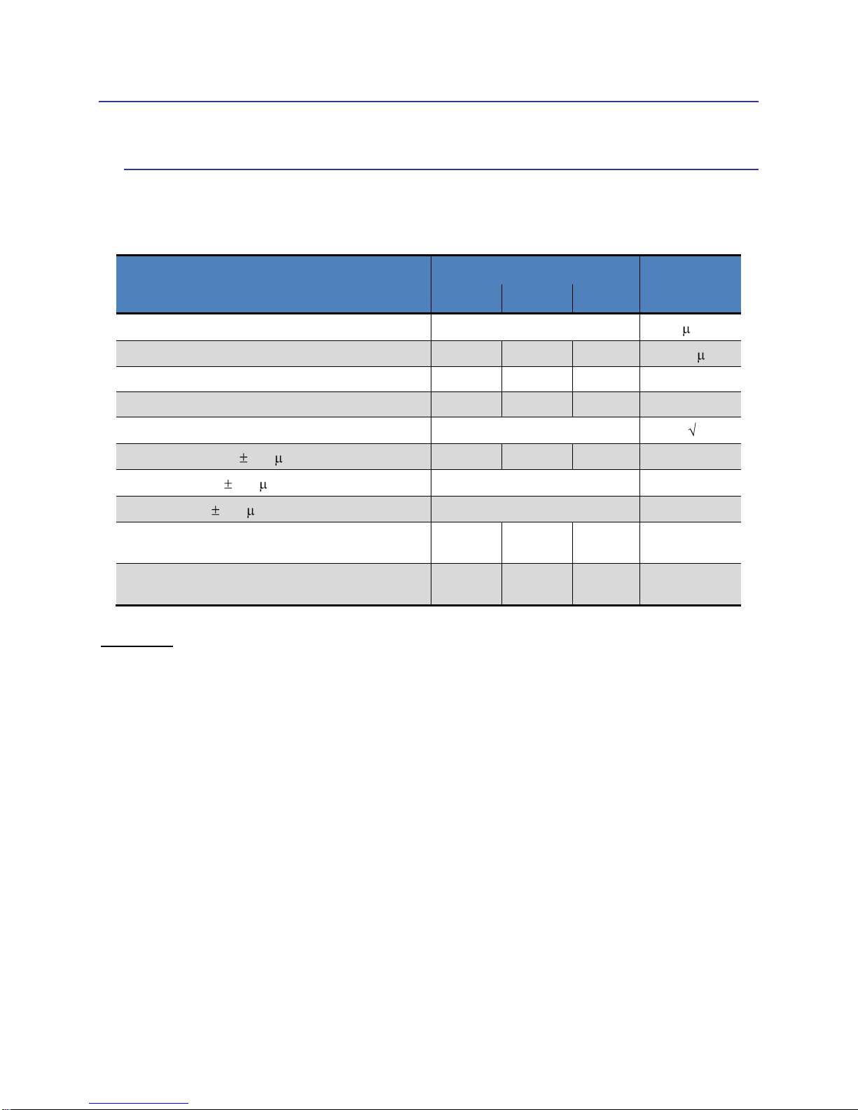
Table 3-1: Operating Performance1
Parameter
Cycle Counts2
Units
50
100
200
Field Measurement Range3
-800 to +800
T
Gain
20
38
75
LSB/ T
Sensitivity
50
26
13
nT
Noise
30
20
15
nT
Noise Density @ Max. Single-Axis Sample Rate
1.2
nT/ Hz
Repeatability over 200 T
15
8
8
nT
Hysteresis over 200 T
15
nT
Linearity over 200 T
0.5
%
Maximum Single-Axis Sample Rate
(divide by 3 for max. 3-axis sample rate)
1600
850
440
Hz
Single-Axis Average Current @ 24 Hz Sample
Rate (equivalent to 3-axis @ 8 Hz)
70
135
260
µA
Footnotes:
1. Specifications are typical and subject to change. Performance specifications established with 3.0
V supply voltage at room temperature.
2. The cycle count values (50 ,100, and 200) are user-configurable and set in the Cycle Count
Registers. See Section 5.1 for how to set the registers.
3. Field measurement range is defined as the monotonic region of the output characteristic curve.

PNI Sensor Corporation Doc 1017252 r02
RM3100 Evaluation Board User Manual Page 6 of 33
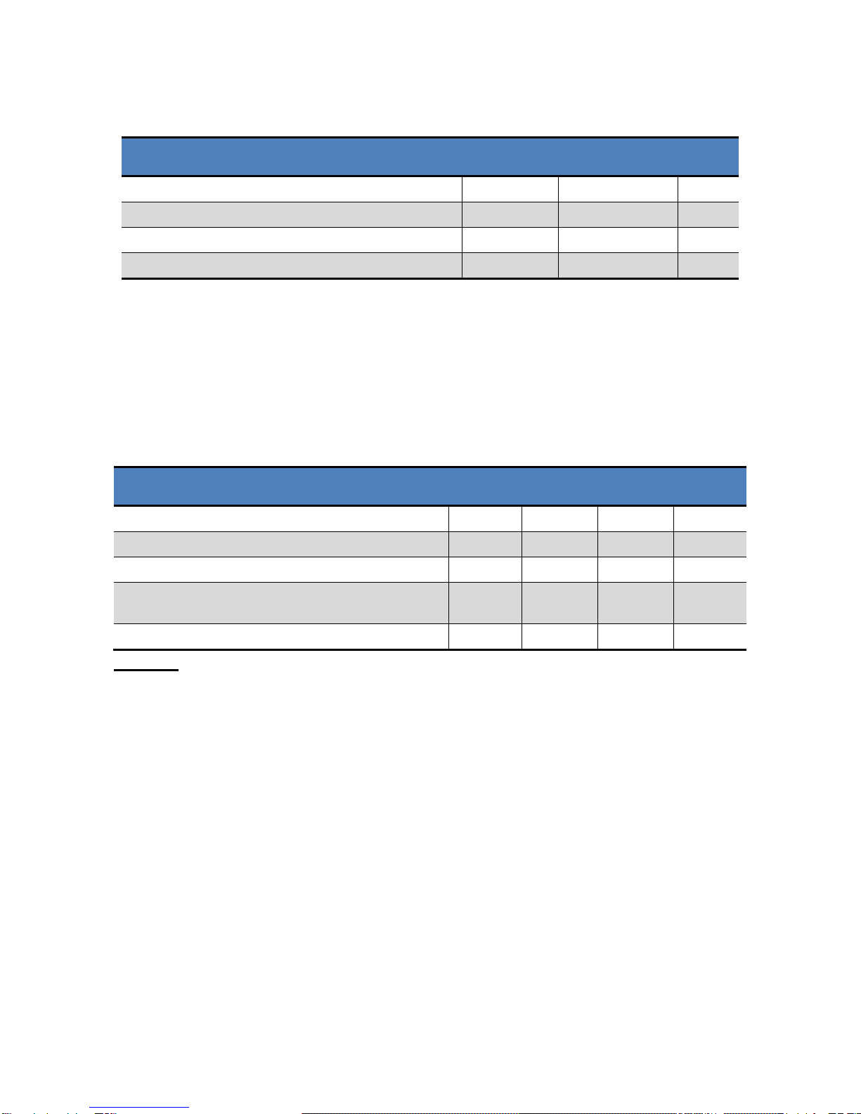
Table 3-2: Absolute Maximum Ratings
Parameter
Minimum
Maximum
Units
Analog/Digital DC Supply Voltage, AVDD & DVDD
-0.3
+3.7
VDC
Input Pin Voltage
-0.3
AVDD or DVDD
VDC
Input Pin Current @ 25C
-10.0
+10.0
mA
Storage Temperature
-40°
+85°
C
CAUTION:
Stresses beyond those listed above may cause permanent damage to the device. These
are stress ratings only. Operation of the device at these or other conditions beyond those
indicated in the operational sections of the specifications is not implied.
Table 3-3: Operating Conditions
Parameter
Min
Typ
Max
Units
Analog/Digital DC Supply Voltage, AVDD & DVDD1
2.0
3.0
3.6
VDC
Voltage Ripple on AVDD or DVDD
0.05
VPP
Idle Mode Current
1
µA
Leakage Current @ DVDD pin
(AVDD=AVSS=DVSS=0V, DVDD=3.6V)
100
nA
Operating Temperature
-40
+85
C
Footnote:
1. Please contact PNI if operation at <2.0 V is required.

PNI Sensor Corporation Doc 1017252 r02
RM3100 Evaluation Board User Manual Page 7 of 33
3.2 Dimensions
Figure 3-1: RM3100 Evaluation Board Mechanical Drawing

PNI Sensor Corporation Doc 1017252 r02
RM3100 Evaluation Board User Manual Page 8 of 33
4 RM3100 Evaluation Board Overview & Set-Up
This section provides an overview of how to set-up the RM3100 Evaluation Board and the basic
I2C and SPI communications requirements. For a discussion of PNI’s magneto-inductive sensor
technology, please refer to either the RM3100 Geomagnetic Sensor User Manual or PNI’s
whitepaper “Magneto-Inductive Technology Overview”, both of which can be found on PNI’s
website at www.pnicorp.com.
4.1 PCB Orientation and Output Polarities
The arrow printed on the RM3100 module indicates the intended line-of-sight. The RM3100
module is arranged in a north-east-down (NED) coordinate system, and the arrow is parallel
to the x-axis sensor. When the module is pointing directly magnetic south the x-axis reading
will be maximized and the y-axis will be zero. Likewise, when the module is pointing west
the y-axis reading will be maximized and the x-axis reading will be zero. The z-axis reading
will depend on the dip angle at the given location. At the geo-magnetic equator, where
Earth’s magnetic field is horizontal, the z-axis reading will be zero when flat.
4.2 Local Magnetic Field Considerations
Because the RM3100 sensor module measures magnetic field, it is important to consider
what items in the vicinity of the module can affect the sensor readings. Note that magnetic
field drops off as (1/distance)3. Specific issues to consider include:
The sensors have a specified linear regime of 200 T. (Earth’s field is ~50 T.) To
ensure the sensors operate in their linear regime, do not place the RM3100 close to
large electric currents, large masses of ferrous material, or devices incorporating
permanent magnets, such as speakers and electric motors.
Locate the RM3100 Eval Board away from changing magnetic fields. If this is not
possible, but the local magnetic field is known to have multiple states, try to take
readings only when the field is in a known state. For instance, if a motor runs part of
the time, take readings only when the motor is in a known state.
If you are uncertain about the effect a specific component may have on the system,
place the RM3100 Eval Board on a firm surface and gradually bring the component in
question close to the board, then note when the magnetic field starts to change. If the
component cannot be moved, then gradually move the RM3100 module towards the
component, carefully ensuring the orientation of the board remains constant while
doing this.

PNI Sensor Corporation Doc 1017252 r02
RM3100 Evaluation Board User Manual Page 9 of 33
4.3 RM3100 Evaluation Board Pin Assignments
The RM3100 Evaluation Board’s pin assignments are summarized below in Table 4-1. Pin
numbers run counterclockwise, when looking from the top, starting at the Pin 1 designator as
shown in Figure 3-1.
Table 4-1: RM3100 Evaluation Board Pin Assignments
Pin#
Pin Name
Description
1
SCK /
SCL
SPI interface (SCK) –Serial clock input
I2C interface (SCL) –Serial clock line
2
SO /
SA1
SPI interface (SO) –Master Input, Slave Output
I2C interface –Bit 1 of slave address
3
SI
SDA
SPI interface (SI) –Master Output, Slave Input Serial Data
I2C interface (SDA) –Serial Data Line
4
SSN /
SA0
SPI interface –Active low to select port
I2C interface –Bit 0 of slave address
5
DRDY
Status line
7
AVSS
Ground pin for analog section of ASIC
10
I2CEN
I2C enable pin (HIGH = I2C, LOW = SPI)
12
DVDD
Supply voltage for digital section of ASIC.
13
AVDD
Supply voltage for analog section of ASIC
14
DVSS
Ground pin for digital section of ASIC
6, 8, 9, 11
NC
Do not connect
4.3.1 General Purpose Pins
DVDD and AVDD (pins 12 & 13)
AVDD and DVDD should be tied to the analog and digital supply voltages,
respectively. The recommend voltages are defined in Table 3-3, and the maximum
voltages are given in Table 3-2. DVDD must be on whenever AVDD is on, so
DVDD should either be brought up first or at precisely the same time as AVDD.
AVDD can be turned off when not making a measurement to conserve power, since
all other operations are supported with DVDD. Under this condition, register values
will be retained as long as DVDD is powered. Also, AVDD must be within 0.1 V of
DVDD when AVDD is on.

PNI Sensor Corporation Doc 1017252 r02
RM3100 Evaluation Board User Manual Page 10 of 33
AVSS and DVSS (pins 7 & 14)
AVSS and DVSS should be tied to the analog and digital ground, respectively.
Assuming the ground plane is clean, they may share a common ground.
Alternatively, they may have their own ground planes if this is more convenient.
DVSS and AVSS should be within 0.1 V of each other.
DRDY (pin #5)
DRDY is used to ensure data is read from the RM3100 Evaluation Board only when
it is available. The DRDY pin will go HIGH when the measurement is complete.
This signals the host that data is ready to be read. The DRDY pin automatically is set
LOW when the Measurement Result registers are read or a write operation is
performed.
It is not mandatory to use the DRDY pin, as alternative methods exist to determine if
data is available. Specifically, the STATUS register provides this information. And,
if using the SPI interface where CPHA=CPOL=1, the MISO line also indicates if data
is available when SSN is LOW.
I2CEN (pin #10)
This pin should be pulled LOW when using the SPI interface or pulled HIGH when
using the I2C interface.
4.3.2 SPI Pins
SCK (pin 1)
SCK is a SPI input used to synchronize the data sent in and out through the MISO
and MOSI pins. SCK is generated by the customer-supplied master device and
should be 1 MHz or less. One byte of data is exchanged over eight clock cycles.
Data is captured by the master device on the rising edge of SCK. Data is shifted out
and presented to the RM3100 Evaluation Board on the MOSI pin on the falling edge
of SCK, except for the first bit (MSB) which must be present before the first rising
edge of SCK.
SO (pin 2)
SO, or for more commonly MISO (master input, slave output), is a SPI output
transmiting data from the RM3100 Evaluation Board to the host. Data is transferred
most significant bit first and is captured by the master device on the rising edge of
SCK. The MISO pin is placed in a high impedance state if the RM3100 Evaluation
Board is not selected (i.e. if SSN=1).

PNI Sensor Corporation Doc 1017252 r02
RM3100 Evaluation Board User Manual Page 11 of 33
SI (pin 3)
SI, or more commonly MOSI (master output, slave input), is a SPI input providing
data from the host to the RM3100 Evaluation Board. Data is transferred most
significant bit first. Data must be presented at least 50 ns before the rising edge of
SCK, and remain valid for 50 ns after the edge. New data typically is presented to the
MOSI pin on the falling edge of SCK.
SSN (pin 4)
This signal sets the RM3100 Evaluation Board as the operating slave device on the
SPI bus. The SSN pin must be LOW prior to data transfer in either direction, and
must stay LOW during the entire transfer.
The SSN pin must transition from HIGH to LOW prior to reading from or writing to
the registers. It must stay LOW for the remainder of the operation.
After communication between the RM3100 Evaluation Board and host is complete,
the SPI bus can be freed (SSN set HIGH) so the host may communicate with other
slave devices while the RM3100 Evaluation Board takes a measurement or is idle.
4.3.3 I2C Pins
SCL (pin 1)
SCL is used to synchronize the data sent between the RM3100 Evaluation Board
(slave) and the host system (master) on the SDA pin. SCL needs to be generated by
the host system and should be 1 MHz or less. Data is captured by the master device
on the rising edge of SCL. Data is shifted out and presented to the RM3100
Evaluation Board on the SDA pin on the falling edge of SCL, except for the first bit
which must be present before the first rising edge of SCL.
SDA (pin 3)
The SDA line is a bi-directional line used to send commands between the RM3100
Evaluation Board (slave) and the host system (master). Data is transferred most
significant bit first. All communication between the host and the RM3100 Evaluation
Board occurs on this line when implementing the I2C interface.
SA0 (pin 4)
SA0 represents the least significant bit in the between the RM3100 Evaluation
Board’s slave address. Pulling this HIGH represents a ‘1’ and pulling it low
represents a ‘0’. Along with pin 3 (bit 1) and the higher 5 bits (0b01000), which are

PNI Sensor Corporation Doc 1017252 r02
RM3100 Evaluation Board User Manual Page 12 of 33
pre-defined in hardware, SA0 establishes the 7-bit slave address of the RM3100
Evaluation Board on the I2C bus.
SA1 (pin 2)
SA1 represents the second-least significant bit in the RM3100 Evaluation Board’s
slave address. Pulling this HIGH represents a ‘1’ and pulling it low represents a ‘0’.
Along with pin 28 (bit 0) and the higher 5 bits (0b01000), which are pre-defined in
hardware, SA1 establishes the 7-bit slave address of the module on the I2C bus.
4.4 SPI Timing Requirements
The RM3100 Evaluation Board can act as a slave device on either a SPI or I2C bus. This
section discusses basic requirements for SPI operation. The SPI interface consists of four
signals, as carried on SCK, (MO)SI, (MI)SO, and SSN. The SPI clock, SCK, should run at
1 MHz or less. Data sent out on MOSI is considered valid while SCK is HIGH, and data is
in transition when SCK is LOW. The first byte sent to the RM3100 Evaluation Board
contains the Read/Write bit (Write=0) followed by the 7-bit register address. When the
register address byte is received the module returns the STATUS register contents.
Assuming SSN stays low and SCK continues, multiple registers can be written to or read
from as the RM3100 Evaluation Board will automatically increment to the next register
address. The clock polarity when the bus is idle can either be LOW (CPOL=CPHA=0) or
HIGH (CPOL=CPHA=1).
As long as SSN is LOW data can transfer to or from the RM3100 Evaluation Board.
Generally it is a good idea to pull SSN to HIGH after a read or write operation has completed
such that the SPI bus can be freed up for other devices. The module can perform
measurements while the SSN line is HIGH, as this does not involve communication with the
master. Pulling the SSN to HIGH during a data read or write will terminate the transaction.
The timing parameters, defined in Figure 4-1 or Figure 4-2 and specified in Table 4-2, must
be met to ensure reliable communication.

PNI Sensor Corporation Doc 1017252 r02
RM3100 Evaluation Board User Manual Page 13 of 33
Figure 4-1: SPI Timing Diagram, CPOL = CPHA = 0
Figure 4-2: SPI Timing Diagram, CPOL = CPHA = 1

PNI Sensor Corporation Doc 1017252 r02
RM3100 Evaluation Board User Manual Page 14 of 33
Table 4-2: SPI Timing Specifications
Symbol
Description
Min
Max
Units
tSHZD
SSN LOW to data output
100
ns
tSSDV
SSN LOW to Command Byte
100
ns
tDBSH
Setup data before active edge
50
ns
tDASH
Hold data after active edge
50
ns
tDRDV
Clock falling edge to valid data
10
ns
tSSH
Final clock cycle falling edge to SSN HIGH
100
ns
tSHDZ
SSN HIGH to output data tri-state
100
ns
tSSW
SSN HIGH to LOW (time between transactions)
100
4.5 I2C Requirements
The RM3100 Eval Board can operate as a slave device on either an I2C or SPI bus. This
section discusses basic requirements for operation on an I2C bus. The module is identified by
a 7-bit slave address, where the higher 5 bits of the slave address are pre-defined in hardware
and the same for all RM3100 Evaluation Boards. PNI has registered these first 5 bits as
0b01000. The lower 2 bits of the slave address are user-configurable, using pins 3 and 28.
As such, 4 different slave addresses are possible. For example, setting pin 3 HIGH and pin
28 LOW results in an address of 0b0100001.
The RM3100 Evaluation Board’s I2C interface complies with NXP’s UM10204 specification
and user manual, revision 03. Standard, fast, fast plus, and high speed modes of the I2C
protocol are supported. Below is a link to this document.
http://www.nxp.com/documents/user_manual/UM10204.pdf
4.5.1 I2C Register Write
A generic Write transaction is given below.
START
RM3100 Eval Board
ADDRESS
RW
ACK
RM3100 Eval Board
REG. ADDRESS (N)
ACK
DATA TO REGISTER (N)
ACK
DATA TO REGISTER (N+1)
ACK
STOP
S
A6
A5
A4
A3
A2
A1
A0
0
0
A7
A6
A5
A4
A3
A2
A1
A0
0
A7
A6
A5
A4
A3
A2
A1
A0
0
A7
A6
A5
A4
A3
A2
A1
A0
0
P
From Host to RM3100 E.B.
------------ Data Transferred (n bytes + acknowledge) ------------
From RM3100 E.B. to Host

PNI Sensor Corporation Doc 1017252 r02
RM3100 Evaluation Board User Manual Page 15 of 33
All communication is on the SDA line. The transaction is initiated by the host, or master,
sending the Start condition followed by the RM3100 Evaluation Board’s slave address,
and then the RW bit is set to ‘0’, indicating a Write operation. The slave address is
acknowledged by the module by setting SDA to LOW. This is followed by the desired 7-
bit register address and then the register data. The register value automatically
increments after every received data byte. The transaction is terminated by the host
sending the Stop condition.
The RM3100 Evaluation Board will always acknowledge the start of an I2C Write
transaction by sending a ‘0’ (i.e. the ACK signal). But if the Write command cannot be
executed for some reason the module will send a ‘1’ instead (i.e. the NACK signal). The
reasons a NACK signal might be sent are established by the HSHAKE register, and
include writing to an undefined register or writing to the POLL register while CMM is in
progress, or vice versa. See Section 5.6.2 for more information.
4.5.2 I2C Register Read
To perform a Read transaction, it is first necessary for the master to Write the desired
register address, and then to Read the register data. A generic transaction is given below.
START
RM3100 Eval Board
ADDRESS
RW
ACK
REGISTER ADDRESS (N)
ACK
STOP
S
A6
A5
A4
A3
A2
A1
A0
0
0
A7
A6
A5
A4
A3
A2
A1
A0
0
P
From Host to RM3100 E.B.
From RM3100 E.B. to Host
START
RM3100 Eval Board
ADDRESS
RW
ACK
DATA FROM REG. (N)
ACK
DATA FROM REG. (N+1)
NACK
STOP
S
A6
A5
A4
A3
A2
A1
A0
1
0
A7
A6
A5
A4
A3
A2
A1
A0
0
A7
A6
A5
A4
A3
A2
A1
A0
1
P
-------------- Data Transferred (n bytes + acknowledge) --------------
The Write sequence is described in the prior section, except for this case there is no data
to send. For the Read sequence the host again sends the RM3100 Evaluation Board’s
slave address, but this time sets the RW bit is set to ‘1’. The module acknowledges that it
is has been addressed and then sends data from the register address that was previously
sent. The host acknowledges receipt of the data, and then the module increments the
register address and sends data from this register. This continues until the host sends the
NACK command followed by the Stop command, which terminates the transaction.

PNI Sensor Corporation Doc 1017252 r02
RM3100 Evaluation Board User Manual Page 16 of 33
5 RM3100 Evaluation Board Operation
The primary functions of the RM3100 Eval Board are:
Set the Cycle Count Registers if the default is not desired.
Initiate either a Single Measurement or Continuous Measurement.
Confirm New Data Ready.
Read the Measurement Results Registers.
Each of these steps is discussed in detail in the following sections.
Note: The RM3100 module incorporates an Idle Mode to reduce power consumption. The device is in
Idle Mode when not exchanging data or taking a measurement. The module powers-up into Idle Mode.
The RM3100 Evaluation Board’s register map is given in Table 5-1. Register addresses are 7
bits. To Write to a register, a ‘0’ followed by the 7-bit register number should be sent, followed
by the register value. To Read from a register, a ‘1’ followed by the 7-bit register number
should be sent, effectively adding 0x80 to the register number.
Table 5-1: RM3100 Evaluation Board Register Map
Name
Register #
(Hex)
R/W
Default
(Hex)
Payload
Format
Description
POLL
00
RW
00
[7:0]
Polls for a Single Measurement
CMM
01
RW
00
[7:0]
Initiates Continuous Measurement Mode
CCX
04 –05
RW
00C8
UInt16
Cycle Count Register –X Axis
CCY
06 –07
RW
00C8
UInt16
Cycle Count Register –Y Axis
CCZ
08 –09
RW
00C8
Uint16
Cycle Count Register –Z Axis
TMRC
0B
RW
96
[7:0]
Sets Continuous Measurement Mode Data Rate
ALLX
0C –0E
RW
000000
Uint24
Alarm Lower Limit –X Axis
AULX
0F –11
RW
000000
Uint24
Alarm Upper Limit –X Axis
ALLY
12 –14
RW
000000
Uint24
Alarm Lower Limit –Y Axis
AULY
15 –17
RW
000000
Uint24
Alarm Upper Limit –Y Axis
ALLZ
18 –1A
RW
000000
Uint24
Alarm Lower Limit –Z Axis
AULZ
1B –1D
RW
000000
Uint24
Alarm Upper Limit –Z Axis
ADLX
1E –1F
RW
0000
UInt16
Alarm Hysteresis Value –X Axis
ADLY
20 –21
RW
0000
UInt16
Alarm Hysteresis Value –Y Axis
ADLZ
22 –23
RW
0000
UInt16
Alarm Hysteresis Value –Z Axis
MX
24 –26
R
000000
Uint24
Measurement Results –X Axis
MY
27 –29
R
000000
Uint24
Measurement Results –Y Axis
MZ
2A –2C
R
000000
Uint24
Measurement Results –Z Axis
BIST
33
RW
00
[7:0]
Built-In Self Test
STATUS
34
R
00
[7:0]
Status of DRDY
HSHAKE
35
RW
1B
[7:0]
Handshake Register
REVID
36
R
--
Unit8
MagI2C Revision Identification

PNI Sensor Corporation Doc 1017252 r02
RM3100 Evaluation Board User Manual Page 17 of 33
5.1 Set the Cycle Count Registers (0x04 –0x09)
The Cycle Count Registers establish the number of sensor oscillation cycles (cycle counts)
that will be counted for each sensor in both the forward and reverse bias directions during a
measurement sequence. Each sensor has its own cycle count value, and each can be
different. Increasing the cycle count value increases measurement gain and resolution.
Lowering the cycle count value reduces acquisition time, which increases maximum
achievable sample rate or, with a fixed sample rate, decreases power consumption. The
Cycle Count read and write addresses, plus their default values, are given in Table 5-2
Table 5-2: Cycle Count Registers
Register Description
Default
Value (Hex)
Write Address
(Hex)
Read Address
(Hex)
X Axis Cycle Count Value - MSB
0x00
04
84
X Axis Cycle Count Value - LSB
0xC8
05
85
Y Axis Cycle Count Value - MSB
0x00
06
86
Y Axis Cycle Count Value - LSB
0xC8
07
87
Z Axis Cycle Count Value - MSB
0x00
08
88
Z Axis Cycle Count Value - LSB
0xC8
09
89
Since the registers are adjacent, it is not necessary to send multiple register addresses, as the
RM3100 Evaluation Board automatically will read/write to the next adjacent register.
The default values for the Cycle Count Registers are 0xC8 in the LSB and 0x0 in the MSB,
or 200D.This default value provides a good trade-off between acquisition time and
resolution, but favors resolution. If the user is more interested in low power consumption or
running at high data rates, a lower cycle count value of (ex. 50Dor 100D) would be more
appropriate. To estimate the appropriate cycle count value for your application review the
specifications given at 50, 100, and 200 cycle counts in Table 3-1. Note that these 3 cycle
counts by no means represent all the cycle count options, as the minimum value is ‘0’ and the
maximum is 65,536. Having said this, quantization issues generally dictate working above a
cycle count value of ~30, while noise limits the useful upper range to ~400 cycle counts.
Assuming a non-default cycle count value is desired, then prior to sending a command to
take a sensor measurement it is necessary to Write values to the Cycle Count Registers.
Once the Cycle Count Registers are set, they do not need to be repopulated unless the user
wants to change the values or the system is powered down, in which case the default value
repopulates the register fields when powered up again.

PNI Sensor Corporation Doc 1017252 r02
RM3100 Evaluation Board User Manual Page 18 of 33
5.2 Initiate Continuous Measurement Mode (0x01)
The RM3100 Evaluation Board can either take measurements automatically on a regular
frequency (Continuous Measurement Mode) or by polling for single measurement. This
section discusses Continuous Measurement Mode. See Section 5.3 for polling a single
measurement.
To initiate Continuous Measurement Mode, write to the CMM register address, 0x01,
followed by the CMM register contents. To set the rate of data acquisition in Continuous
Measurement Mode, see Section 5.2.1. Below are the contents of the CMM register.
Bit #
7
6
5
4
3
2
1
0
Value
LDM
CMZ
CMY
CMX
DRDM1
DRDM0
ALARM
START
Where:
START –A “1” in this bit position initiates Continuous Measurement Mode. To turn
off Continuous Measurement Mode it is necessary to write a “0” to this bit position.
Note that writing to POLL (i.e. initiating a single measurement command) while
operating in Continuous Measurement Mode results in the single measurement
command being ignored.
ALARM –A feature of the RM3100 Evaluation Board while operating in Continuous
Measurement Mode is the ALARM bit will go HIGH if a measurement reading is
outside a predefined range of values, set by the Alarm Upper and Lower Limit
Registers. This bit is set to ‘1’ if a limit is exceeded. The ALARM bit is reset by
writing a ‘0’ to this bit. See Section 5.2.2 for additional information.
DRDM –These two bits establish the required condition to trigger the DRDY pin to
HIGH. There are 4 possible conditions, as set out in Table 5-3.

PNI Sensor Corporation Doc 1017252 r02
RM3100 Evaluation Board User Manual Page 19 of 33
Table 5-3: Continuous Mode DRDY Options
DRDY Requirements
DRDM1
DRDM0
DRDY to HIGH when ALARM = 1, AND a full
measurement sequence is completed, as
established by CMX, CMY, and CMZ.
0
0
DRDY to HIGH after the completion of a
measurement on any axis.
0
1
DRDY to HIGH after a full measurement
sequence is completed, as established by
CMX, CMY, and CMZ.
1
0
DRDY to HIGH when Alarm = 1.
1
1
CMX, CMY, CMZ –A “1” in either of these three bit positions indicates a
measurement will be taken on that sensor axis when operating in Continuous
Measurement Mode. For instance, to take measurements on all three axis, CMX =
CMY = CMZ = 1.
LDM –This bit indicates whether Absolute or Relative Alarm Mode is being
implemented. A “0” indicates Absolute Alarm Mode, while a “1” indicates Relative
Alarm Mode. See Section 5.2.2 for additional information.
To read from the CMM register, send 0x81. The return byte will provide the same
information as above, specifically indicating if ALARM is HIGH.
Note: Certain commands, such as reading from the CMM register or writing to the TMRC register,
will stop Continuous Measurement Mode.
5.2.1 Setting the CMM Update Rate with TMRC (0x0B)
The time between measurements in Continuous Measurement Mode is established with
the TMRC register. The TMRC register is defined below.
Bit #
7
6
5
4
3
2
1
0
Value
1
0
0
1
TMRC3
TMRC2
TMRC1
TMRC0
The LSB is used set the CMM updatee rate. The MSB should be 0x9, as indicated above.
The larger the TMRC value, the longer the interval between measurements. Available
data rates are given in Table 5-4. Note that the update rates are approximate, and have a
one standard deviation tolerance of about ~7%. The default value for TMRC is 0x96,
establishing a data update rate of ~37 Hz.
Other manuals for RM3100
1
Table of contents
Other PNI Motherboard manuals