Contents
1 INTRODUCTION ....................................................................................................................................... 3
F
EATURES
.................................................................................................................................................... 3
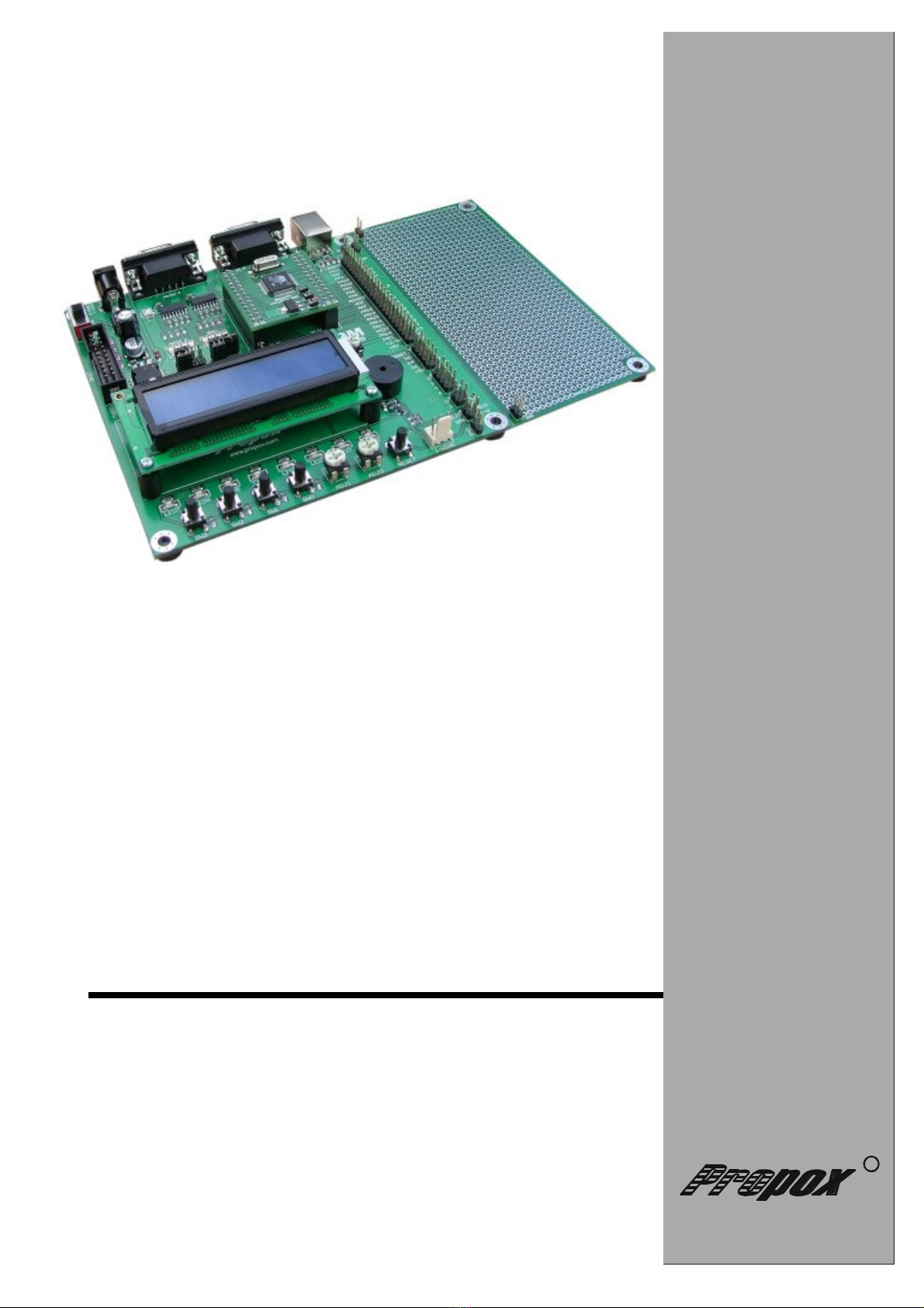
2THE BOARD.......................................................................................................................................... 4
P
LACEMENT OF ELEMENTS ON THE BOARD
................................................................................................. 4
A
RRANGEMENT OF LEAD
-
OUTS
.................................................................................................................... 5
B
OARD CONFIGURATION
.............................................................................................................................. 5
B
OARD SUPPLY
............................................................................................................................................ 7
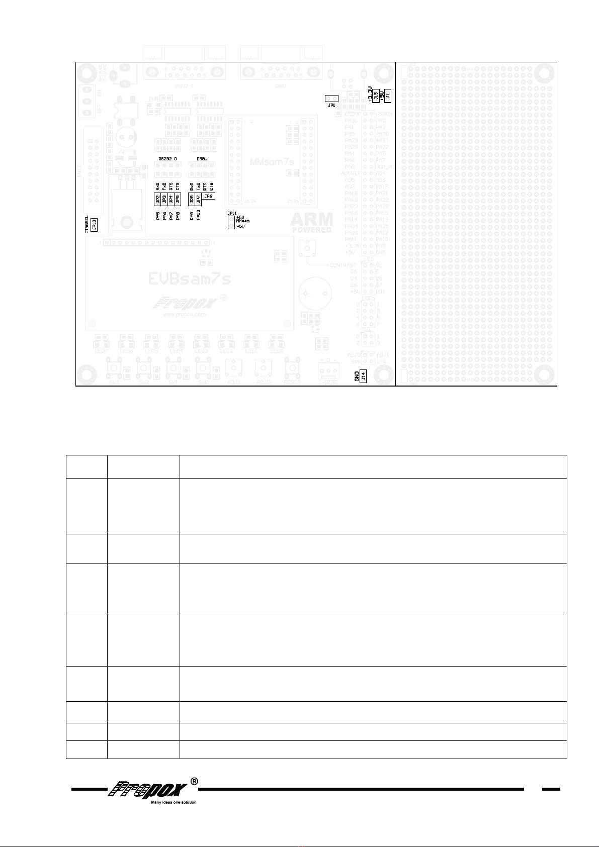
LED
DIODES
................................................................................................................................................. 7
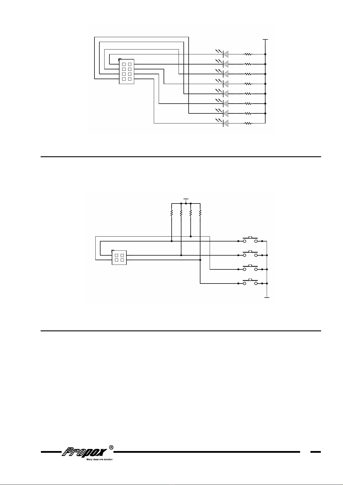
P
USH
-
BUTTONS
............................................................................................................................................ 8
LCD
DISPLAY
............................................................................................................................................... 8
P
OTENTIOMETERS
........................................................................................................................................ 9
B
UZZER
........................................................................................................................................................ 9
RESET
BUTTON
........................................................................................................................................ 10
RS-232
INTERFACES
................................................................................................................................. 10
USB
INTERFACE
........................................................................................................................................ 11
1-W
IRE INTERFACE
.................................................................................................................................... 12
JTAG
CONNECTOR
.................................................................................................................................... 12
3TECHNICAL ASSISTANCE ............................................................................................................. 13
4GUARANTEE ...................................................................................................................................... 13
5BOARD LAYOUT AND DIMENSIONS ........................................................................................... 14
6SCHEMATIC........................................................................................................................................ 14