TABLE
OF
CONTENTS
....................................................
Interface
••••••••••••••••••••••••••••••••••••••••••
I
NSTAlLATI
ON
•.•.•.••••••••••••••••••••••••••••••••••••.••••.•••
I
NTRODUCTI
ON
•••••••••••••••••••••••••••••••••••••••••••••••••••
Page
1
1
1
2
3
3
3
3
3
3
4
5
5
7
7
7
8
8
8
9
9
9
9
9
10
10
10
10
10
11
11
11
12
13
13
13
15
15
17
17
18
18
18
18
iii
Interface
••••••••••••••••••••••••••••••••••••••••
....................................................
Input Lines
.....•.........•.•...........•........•..........
Drive Select 1-4
••••••••••••••••••••••••••••••••••••••••
Direction .
Step
............................•.......................
Write
Data
••••••••••••••••••••••••••••••••••••••••••••••
Write
Gate
•••.•..•••.••••••••••.•.••••••••.••.•.••••••••
Side Select
•••••••••••••••••••••••••••••••••••••••••••••
Low
Current/Switch
Filter
•••••••••••••••••••••••••••••••
Head
Load
•••••••
·
••••••••••••••••••••••••••••••••••••••••
In
Use
••••••••••••••••••••••••••••••••••••••••••••••••••
Output
Lines
••••••••••••••••••••••••••••••••••••••••••••••••
Index .
Rea
dy
•••••••••••••••••••••••••••••••••••••••••••••••••••
Track
OO
•••••••••••••••••••••••••••••
~
••••••••••••••••••
Write Protect
•••••••••••••••••••••••••••••••••••••••••••
Read
Data
••.••••••••••••••••.•••••••••••••••••••.•••.••.
Disk
Change
•••••••••••••••••••••••••••••••••••••••••••••
Two-S
i
ded
•••••••••••••••••••••••••••••••••••••••••••••••
Alternate
I/O
Pins
••••••••••••••••••••••••••••••••••••••••••
Scope
of
Manual
•••••••••••••••••••••••••••••••••••••••••••••
General Description
•••••••••••••••••••••••••••••••••••••••••
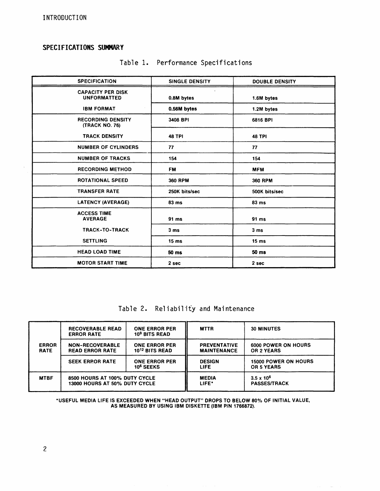
Specifications
Summary
••••••••••••••••••••••••••••••••••••••
Compati
bi
1
ity
•••••••••••••••••••••••••••••••••••••••••••••••
Read/Write/Erase
Head
•••••••••••••••••••••••••••••••••••
Read
Output
Level
•••••••••••••••••••••••••••••••••••••••
Write Current
•••••••••••••••••••••••••••••••••••••••••••
Switch
Filter
•••••••••••••••••••••••••••••••••••••••••••
Track
Positioning
•••••••••••••••••••••••••••••••••••••••••••
Index Positioning
•••••••••••••••••••••••••••••••••••••••••••
Receiving
and
Inspection
••••••••••••••••••••••••••••••••••••
Mou
nt
in
g
....•.•••••••••••••••••••.•.••••••••••••••.•..••••••
Mechanical
Dimensions
•••••••••••••••••••••••••••••••••••
Recommendations
•••••••••••••••••••••••••••••••••••••••••
Installation
Requirements
•••••••••••••••••••••••••••••••••••
Timing
Physical
Connectors
and
Cables
•••••••••••••••••••••••••••••••••••••••
I/O
Signals
(Pl/Jl)
•••••••••••••••••••••••••••••••••••••
Power
(P5/J5)
•••••••••••••••••••••••••••••••••••••••••••
T
ermi
nators
•••••••••••••••••••••••••••••••••••••••••••••••••
INTERFACE
El
ectri
cal