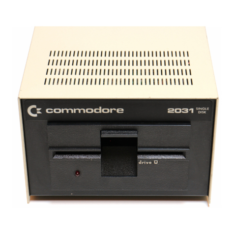
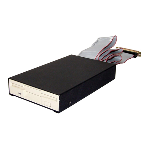
Shugart SA400L Minifloppy User manual

SA400L Minifloppy™
Diskette
Storage
Drive
Shugar
m
2D
I—'

TABLE
OF
CONTENTS
Page
TABLE
OF
CONTENTS
i
LISTOFHGURES
iii
LIST
OF
TABLES
v
ABBREVIATIONS/MNEMONICS
v
SECTION! INTRODUCTION M
1.1 General
Description
l-l
1.2
Specification
Summary
1*1
1.2.1 Performance
Specifications
1-1
1.2.2
Functional
Specifications
1-1
1.2.3
Physical
Specifications
1*2
1.2.4
Reliability
Specifications
1-2
SECTION
II
ELECTRICAL
INTERFACE
2-1
2.1 General 2-1
2.2
Signal
Interface
2-2
2.3 PowerInterface 2-2
2.4
Input/Output
Lines
2-2
2.5 FrameGround 2-2
SECTION
III
PHYSICAL
INTERFACE
3-1
3.1
General
3.2
J1/PIConnector
^5
3.3
J2/P2
Connector
3.4
Frame Grounding
SECTION
IV
THEORY
OF
OPERATION
J
4.1
General
Operations
4.2
Head
Positioning
"2
4.3
Diskette
Spindle
Drive
J o
4.4
Read/Write
Head
4.5
Recording Format
4.5.1
General
4.5.2
Byte
4.6 Formats ^ o
4.6.1
Soft Sectored Recording Format
4.6.2
Track Layout
'e
4.6.3
Hard Sectored Recording Format
4.7
Drive Motor Control
4.7.1
Head
Load
4.7.2
Single DriveSystem
4.7.3
MultipleDriveSystem
4.8
Index Detector
4.9
Track
Zero
Indication
4.10
Track
Accessing
4.10.1 Stepper Motor "o
4.10.2 StepperControl -«
4.11
Read/Write
Operations
4.12
Read/Write
Head
,2
4.13
WriteCircuitOperation
4.14 Read
Circuit
Operation ^
4.15
Write
Protect
SECTION
V
MAINTENANCE
l'\
5.1
Maintenance
Equipment
e ,
5.1.1 AlignmentDiskette
5.1.2
Exerciser
5.1.3
Special Tools

5.2
Diagnostic Techniques 5-1
5.2.1
Introduction 5-1
5.2.2
Soft Error Detection
and
Conection
5-2
5.2.3
Write Error
5-2
5.2.4
Read
Error
5-2
5.2.5
Seek
Error
5-2
5.2.6 InterchangeError 5-2
5.3
Removalsand Replacements 5-3
5.3.1
Faceplate
5-3
5.3.2
DriveMotor Assembly 5-3
5.3.3
StepperMotor
and
Actuator
Cam
5-3
5.3.4
Head
and
Carriage Assembly
5-3
5.3.5
Clamp
Hub
5-3
5.3.6
Hub Frame Assembly
5-4
5.3.7
Write
Protect
Switch
5-5
5.3.8
Index Detector Assembly 5-5
5.3.9
Index
LED
5-5
5.3.10
Track
Zero
Switch
5-5
5.4
Check. Adjustments, and Alignment 5-5
5.4.1
Test
Point
Locations
5-5
5.4.2 Head
Amplitude
Check 5-6
5.4.3
Motor
Speed Adjustment 5-7
5.4.4
Motor
Speed Adjustment
(Using
aFrequency Counter) 5-7
5.4.5 Track
GO
SwitchAdjustment 5-7
5.4.6
Carriage
Limiter
5-9
5.4.7 Index
Timing
Adjustment
(Soft
Sector)
5-9
5.4.8 Index/SectorTiming
Adjustment
(Hard
Sector)
5-10
5.4.9 Head/Radial
Alignment
5-10
5.4.10
Write
Protect
Switch
Adjustment
5-12
5.4.11 Read/Write Head
Cleaning
Procedure 5-12
5.5
Receiving
Inspection
5-13
5.5.1
Philosophy
5-13
5.5.2 Procedure 5-13
SECTION
VI
MAINTENANCE
DIAGRAMS
5-1
SECTION
VII
ILLUSTRATED
PARTS
CATALOG
7-J
7.1
Description
7.2 Cablesand CableConnections 7-1
7.3
Recommended
Spare
Parts
Stocking
Guide
7-1

LIST
OF
FIGURES
Figure Title Page
1-0 SA400LDrive 1-0
2-1 Interface Connections 2-1
2-2 InterfaceSignal Driver/Receiver 2-3
3-1 InterfaceConnectors - PhysicalLocations 3-1
3-2
J1
Connector
Dimensions
3-2
3-3
J2
Connector
3-2
4-1 Functional Diagram 4-1
4-2 Byte (FMEncoding) 4-3
4-3
Recommended Soft SectorSingle Density (Even Boundaries)
(FM)
4-3
4-4
MFM
Recommended Format.
256
Bytes/16Records Per Track
(IBM
Type) 4-4
4-5
Recommended
Hard
Sector
FM
and
MFM
Formats
4-5
4-6
Motor Control Functional Diagram 4-6
4-7
Drive Select Functional Diagram
4-6
4-8
Index Detector Logic 4-7
4-9
Index Timing Diagram 4-7
4-10
Track
GO
Indication Diagram
4-8
4-11 Track
(X)
Timing Diagram 4-8
4-12 StepperControl Functional Diagram 4-9
4-13 Step TimingDiagram 4-9
4-14
Bit
Cell
4-10
4-15
Basic
Read/Write
Head
4-11
4-16
Recorded
Bit
4-11
4-17 Readinga Bit 4-11
4-18 IF and 2FRecordingRux and PulseRelationship 4-12
4-19
Read/Write
Head
4-12
4-20
Write
Circuit FunctionalDiagram 4-13
4-21 Read Circuit FunctionalDiagram 4-14
4-22
Write
ProtectFunctional
Diagram
4-14
5-1 HubFrameAdjustment 5-4
5-2
Test Point Locations
5-6
5-3
Motor
Speed Adjustment 5-7
5-4
TrackZero Position
5-8
5-5 TrackZero
Switch
Adjustment 5-8
5-6
Carriage
Limiter
Clearance 5-9
5-7 IndexDetector Adjustment 5-10
5-8 SA400L Service Position 5-11
5-9
Index
Timing
5-11
5-10
Correct
Head
Radial
Alignment
5-12
5-11
Head
Radial
Alignment
5-12
5-12
Write
Protect
Switch
Adjustment
5-13
6-1
Write
Protect
Inoperative
5-1
6-2
Diskette
Not
Rotating
5-2
6-3
Track
(X)
Indicator
Inoperative
5-3
6-4
Drive
Not
Coming
On
Line
5-4
6-5
Index
Pulse
Inoperative
5-5
6-6
Drive
PCB
Logic
Diagram
5-6
6-7 Read/Write
Logic
Diagram
5-6
6-8
Write
Protect
Logic
Diagram
5-6
6-9
Motor
Speed
Control
Logic
Diagram
5-6
6-10
Power
Diagram
5-7
6-11 400L (40
Track)
Read/Write Schematic
Diagram
(2sheets) 6-9
7-1
SA400L
Exploded
View
7-2
7-2 DrivePCB Parts Location (P/N 25210) 7-4
7-3 Track
00
Switch Parts Location 7-7
7-4 Carriage/Head
Parts
Location
7-8
7-5 Hub Frame Parts Location 7-9
7-6
Head
Load Solenoid Parts Location 7-10
ill

LIST
OF
TABLES
Table
Title
Page
2-1
DC
Power
2-2
7-1
P/N
to Figure - Reference 7-11
7-2
Cable
and
Cable
Connections
Part
Numbers
7-12
7-3 Spare Parts Stocking Guide 7-13
ABBREVIATIONS
/
MNEMONICS
bp!
Bits
per
Inch
NHA
Next Higher Assembly
CK
Clock
NRZ
Non-Return
to
Zero
CRC
Cyclic Redundancy Check
R/W
Read/Write
fcl
Flux Changes
per
Inch
tpi
Tracks per Inch
FM
Frequency Modulation
TRK
Track
ID
Identification
WG
OFF
Write
Gate
Off
IFC
illustrated Parts
Catalog
WP
Write
Protect
MFM
Modified
FM
2F
Double
Frequency
NHA
Next Higher Assembly
ABOUT
THIS
MANUAL
While
every
effort
has
been
made
to
ensure
that
the
information
provided
herein
is
correct,
please
notify
us
in
the
event
ofan
error
or
inconsistency.
Write
any
comments
on
the
form
in
the
back
of
this
manual
and
send
to.
Shugart
Technical
Publications.
MS
3-14
475
Oakmead
Parkway
Sunnyvale. CA
94086
(408)
733
()l(n)
This
manual
(P/N
39028-1)
supersedes
and
makes
obsolete
the
previous
edition
of
this
manual
(P
N
39028-0.
dated
5/81).
IV

39028-46
FIGURE
1-0.
SA400L
DRIVE

SECTION
1
INTRODUCTION
1.1
GENERAL
DESCRIPTION
This manual provides depot level maintenance information necessary to maintain, trouble-shoot, and repair the
SA400L Minifloppy diskdrive manufactured by Shugart. Aseparate OEM manual (SA400LOEM
P/N
39019) is
available which describes the installation, interface,
and
power requirements useful for the applications of the
SA400L.
The SA400L floppy drives have these standard features:
a. Compact size
and
weight similar to most tape cassette units.
b. Single and double density capability.
c.
125/250
k bytes (unformatted) storage capacity.
d.
125/250
k
bits/second
transfer
rate.
e. Low
heat
dissipation.
f. Positive media insertion to avoid media
damage.
g.
EK^
drive motor (eliminates ac requirements).
h. Proprietary read/write head
designed
and manufactured byShugart.
i. Write protect circuitry,
j. Activitylight.
1.2
SPECIFICATION
SUMMARY
1.2.1
Perfomance
Specificatlona
Capacity
Single Density Double Density
(in
bytes)
(FM)
(MFM)
Unformatted
Per
Disk
125,000 250,000
Formatted
(16
Records/Track)
Per
Disk
81.920 163,840
Per Track 2,048 4,096
Per Sector 128 256
Formatted
(10
Records/Track)
Per
Disk
102,400 204,800
Per Track 2,560 5,120
Per Sector 256 512
TransferRate 125 k bits/sec. 250 k bits/sec.
Latency
(avg.)
100 ms
Access
Time
Track-to-Track
20
ms
Average
286 ms
Settling Time 20 ms
1.2.2
Functional
Specifications
RotationalSpeed 300 rpm
Recording
Density
2768
bpi
(FM)
5536
bpi
(MFM)
Flux
Density
5536
fci
(FM)
5536
fci
(MFM)
Track
Density
48 tpi
1-1

Media Requirements
SA104
(soft-sectored)
SA105
(16 sectors, hard-sectored)
SA107
(10 sectors, hard-sectored)
Industry standard flexible diskette
Oxide on 0.(X)3 in. (0.08 mm)
Myleur
5.25
in.
(133.4
mm)
square
jacket
1.2.3
Physical
Speclficadons
Operatiiig
Shlppiii9
Storage
Environmental
Limits
Ambient Temperature
50®
to
115®F
—40®
to
144®F
—8®
to
117®F
(10.0® to 46.1®C)
(-40®
to
62®C)
-22®
to
47'C)
Relative Humidity 20 to 80% 1 to 95% 1 to 95%
Maximum
Wet
Bulb 85®F (29.4®C) No
Condensation
No
Condensation
DC Voltage Requirements
+12
V ±
5%
@
1.80
A
max
-I-
5 V ±
5%
@
0.70
A
max
Mechanical Dimensions (exclusive of front panel)
Width
=
5.75
in.
(146.1
mm)
Height =
3.25
in. (82.6 m,m)
Depth =
8.25
in. (209.6 mm) Nominal
Weight = 3 lbs. (1.36 kg) Nominal
Power
Dissipation
13.3
Watts (45.3
BTU/hr)
Continuous (typical)
7.3
Watts (24.9 BTU/hr) Standby (typical)
1.2.4
Reliability
Specificatioiis
Mean Time Between Failure: 8000 power on hours at 25% duty
cycle
Mean Time to Repair:
30
minutes
Error
Rates:
Soft Read Errors: 1 per
10'
bits read.
Hard Read Errors: 1 per
10"
bits read.
Seek Errors: 1 per
10®
seeks
Media
Life:
Passes per Track:
3.0
x
10®
Insertions: 30,(X)0+
1-2

SECTION
II
ELECTRICAL
INTERFACE
2.1
GENERAL
The electrical interfacebetween the SA400L drive and the host system is viatwo connectors. The
first
connector,
Jl,
provides
the
signal
interface
(see
figure
2-1). The second connector, J2,
provides
the dc power.
Frame
ground is connected vai a faston connector located at the rear of the casting.
DRIVE
HOST
SYSTEM
SPARE
SIGNAL
LINE
Jl
21
SPARE
SIGNAL
LINE
4
DRIVE
SELECT
4^6 , 3
^INDEX/SECTOR
8 , 5
DRIVE
SELECT
1^10 ,' 7
DRIVE
SELECT
212 1' 9
.11
DRIVE
SELECT
3
14
MOTOR
ON
^
16
>
1J
DIRECTION SELECT ^
18
•ID
'17
'19
STEP
^20 ,
WRITE
DATA
^
22
WRITE
GATE
^
24
'41
'23
^
TRACK
00
26
^
WRITE
PROTECT
28 ,
'4D
^READ
DATA
30
SPARE
SIGNAL
LINE
32
SPARE
SIGNAL
LINE
34
•.Jl
»33
+
5VDC
»•
J2
4
+12VDC
^1
• 3
, 0
n7^
FRAME
"=
GROUND
FIGURE 2-1. INTERFACE
CONNECTIONS
2-1

2.2
SIGNAL
INTERFACE
Connection to J1 is through a
34
pin PCB edge card connector. The pins are numbered 1through
34
with the
even numbered pinson the component sideofthe PCB. The odd numberedpinsare on the non-componentside.
Pin 2 is located on the
end
of the PCB connector closest to the
comer
and
is labeled 2. A key slot is provided be
tween pins 4
and
6 for optional connector keying.
2.3
POWER
INTERFACE
DC power to the drive is via connector
P2/J2
which is located on the non-component side of the drive PCB near
the spindle drive motor. The drive uses two voltages. Table 2-1 outlines the voltage and current requirements.
TABLE
2-1.
DC
POWER
P2
PIN
1
DC
VOLTAGE
-I-
12VDC
+
12
Return
+ 5
Return
+ 5
VDC
TOLERANCE
±0.6
VDC
±0.25
VDC
CURRENT
*1.80
A
MAX
0.90
A
TYP
0.70
A
MAX
0.50
A
TYP
MAX
RIPPLE (p
to
p)
100
mV
50
mV
•THE 12Vdc
CURRENT
IS
COMPOSED
OF THREE
COMPONENTS;
HEAD
LOAD
CURRENT,
DISKETTE
DRIVE
MOTOR
CURRENT.
AND
PCB
FUNCTIONS.
EACH
OF THESE
COMPONENTS
HAS THE
FOLLOWING CONTRIBUTIONTO THE 12 Vdc CURRENT REQUIREMENTS.
1. PCB
FUNCTIONS
(DRIVE
"STANDBY"
CURRENT)
—0.4A
TYP;
0.5 A
MAX
2.
HEAD
LOAD
(DRIVE
SELECTED)
-0.16
A
TYP;
0.2 A
MAX
3.
DRIVE
MOTOR: START(FOR 400
ms
MAX)
—1.0 A TYP; 1.1 A
AMX
RUNNING
0.36
A
TYP;
1.1
A
MAX
(MOTOR
STALLED)
38028-17
2.4
INPUT/OUTPUT
UNES
There
are
four
output
lines
from
the
SA400L.
The
output
signals
are
driven
with
an
open
collector
output
stage
capable
of
sinking
a
maximum
of
48
mA
at
a
logical
zero
level
or
true
state
with
a
maximum
voltage
of
0.4
V
measured
atthe
driver.
When
the
line
driver
isa
logical
oneor
false
state
the
driver
is
off
andthe
collector
cunentis
amaximum of
250
/lA.
There
are
nine
Input
lines
to
the
SA400L.
See
figure
2-2
for
the
recommended
circuit.
These
input
lines
have
the
following
electrical specifications.
True
=
Logical
zero
=
Vin
± 0.0 V to +0.4 V @
lin
= 48
mA
(max)
False
=
Logical
one =
Vin
+ 2.5 Vto +5.25 V
I®
lin
=
250/lA
(open)
Input Impedance = 150 ohms
2.5
FRAME
GROUND
It
is
important
that
the
drive
be
frame
grounded
to
the
host
system
ac
ground
or
frame
ground.
Failure
to
do
so
may
result
in
drive
noise
susceptibility.
Refer
to
paragraph
3.4
for
the
procedure.
2-2

MAX
10
FEET
RIBBON
OR
ISTED
PAIR
I M/
—H
Rl
rrw
150
0
39028-2S
FIGURE
2-2.
INTERFACE
SIGNAL
DRIVER/RECEIVER
2-3/2-4 (blank)

SECTION
ill
PHYSICAL
INTERFACE
3.1
GENERAL
This
section
describes
the
physical
connectors usedon the
drive
and therecommendedconnectors to be used
with
them. See figure 3-1 for connector locations.
Drive
PCS
Frame
Connector
Amp P/N 60972-1
J1
Frame
Ground^s^^
>
Amp
P/N
61664-1
P1
Connector
Scotchflex
P/N
3463-0001
or
Amp P/N 583717-5
Amp P/N 350211-1
P2
Connector
AmpP/N 1-480424-0
3902S-1S
FIGURE
3-1.
INTERFACE
CONNECTORS•
PHYSICAL
LOCATIONS

3.2
J1/PI
CONNECTOR
The dimensions for the J1 connector are shown in figure 3-2.
0.036
±
0.004-
KEY
SLOT
0.450
±0.010
0.050"
NOM
0.050"
NOM
1.795
±0.005
0.100"
NOM
BOARD
THICKNESS
0.062
±
0.007"
FIGURE
3-2.
J1
CONNECTOR
DIMENSIONS
The
recommended
connectors
for
PI
are
tabulated
below:
0.063"
NOM (2X)
382304)7
TYPE
OF
CABLE
MANUFACTURER
CONNECTOR
P/N
CONTACT
P/N
Twisted
Pair,
#26
AMP
583717-5
1-583616-1
Flat
Cable
3M
"Scotchflex"
34634X)01
NA
3.3
J2/P2
CONNECTOR
The
dc
power
connector,
J2,
is
mounted
on
the
non-component
side
of
the
PCB
and
is
located
near
the
drive
motor.
J2
is
a
4-pin
AMP
Mate-N-Lok
connector,
P/N
350211-1.
The
recommended
mating
connector
(P2)
is
AMP
P/N
1-480424-0,
using
AMP
pins
P/N
61473-1.
J2,
pin
1,
is
labeled
onthe
component
side
of
the
PCB.
Wire
used
should
be
<^18
AWG.
Figure
3-3
illustrates
J2
connector
as seenon the
drive
PCB
from
the
non-
component side.
+
12
VDC
00
0
0—
VDC
39211-16
FIGURE
3-3.
J2
CONNECTOR
3.4
FRAME
GROUNDING
The
SA400L
must
be
frame-grounded
to
the
host
system
to
ensure
proper
operation.
If
the
frame
of
the
drive
is
not
fastened
directly
to
the
frame
of
the
host
system
with
a
good
ac
ground,
a
wire
from
the
system
ac
frame
ground
must
be
connected
to
the
SA400L.
For
this
purpose,
a
faston
tab
is
provided
on
the
drive
at
the
rear
of
the
casting
where
a
faston
connector
can
be
attached
or
soldered.
The
tab
is
AMP
P/N
61664-1
and
the
mating
con
nector is AMP
P/N
60972-1 (see figure 3-1).
3-2

SECTION
IV
THEORY
OF
OPERATION
4.1
GENERAL
OPERATIONS
The SA400L
Minifloppy
Drive
consists
of read/write and controlelectronics,
drive
mechanism, motor control,
read/write head, and track
positioning
mechanism. These componentsperform the
following
functions.
a. Interpret and generate control signals.
b.
Move
read/write
head
to
the
desired
track.
c.
Read
and
write
data.
d. Maintain correct diskette
speed.
The relationship and interface
signals
for the internal functions of the SA400Lare shown in
figure
4-1.
The Head Positioning ActuatorCam positionsthe read/write head to the desired track on the diskette.
WRITE
PROTECT
(COM!
^EAD
DATA
READ
LOGIC
DRIVE
SELECT
WRITE
DATA
WRITE
GATE
WRITE
PROTECT
WRITE
LOGIC
DRIVE
SELECT
STEP
DIRECTION
SELECT
DRIVE
SELECT
(4
LINES^
,TRACK
00
,INDEX/SECTOR
MOTOR
ON
CONTROL
LOGIC
WRITE
PROTECT
READ
HEAD
WRITE
HEAD
ACTIVITY
LIGHT
HEAD
LOAD
SOLENOin
TRACK
00
(COM)
TRACK
00
(N/Oi
MOTOR
CONTROL
TACHOMETER
STEPPER
OA
STEPPER
OB
STEPPER
OC
STEPPER
OD
INDEX/SECTOR
DETECTOR
INDEX/SECTOR
LED
FIGURE
4-1.
FUNCTIONAL
DIAGRAM
4-1
WRITE
PROTECT
SWITCH
INDEX/SECTOR
DETECTOR
INDEX/SECTOR
LED
TEPPER
MOTOR
TRKOO
SWITCH
DRIVE
MOTOR

The electronics packaged on the drive PCB contains:
a.
Index
Detector
circuits
b.
Head
Position
Actuator
Driver
c. Read/Write Amplifier
and
Transition Detector
d. Step Control Logic
e. Track Zero Sensing circuits
f. Write
Protect
circuitry
g. Motor
on/off
circuitry
h. Motor speed control
4.2
HEAD
POSITIONING
An
electrical
stepping
motor
drives
the
Head
Position
Actuator
Cam
which
positions
the
read/write
head.
The
stepping
motor
rotates
the
actuator
cam
clockwise
or
counter-clockwise.
The
using
system
increments
the
step
ping
motor
to
the
desired
track.
Each
step
consists
of
two
steps
to
the
stepper
motor
for
each
step
pulse
supplied
on
the
interface.
4.3
DISKETTE
SPINDLE
DRIVE
The
diskette
dc
drive
motor
rotatesthe
spindle
at300rpmthrough a
belt-drive
system.
50 or60 Hzoperation isac
commodated
without
any
changes.
A
Clamping
Hub
moves
in
conjunction
with
the
hub
frame
that
precisely
clamps
the
diskette
to
the
spindle
hub.
The
motor
is
started
by
making
the
interface
signal
MOTOR
ON
true
and
is
stopped by makingthis signalfalse.
4.4
READ/WRITE
HEAD
The read/write head is
ceramic
and in
direct
contact
with
the diskette. The head surface hasbeen designed to ob
tain
maximum
signal
transfer
toand
from
the
magnetic
surface
ofthe
diskette
with
minimum
head/diskette
wear.
The
SA400L
ceramic
head isa
single
element
read/write head
with
straddle
erase
elements
to
provide
erased
areas between data tracks. Thus, normaltolerance between media and drives
will
not degrade the signalto noise
ratio
and
ensures diskette interchangeability.
Theread/write
head
is
mounted
on a
carriage
which
is
located
onthe
Head
Position
Actuator
Camandis
driven
through
a
cam
follower.
The
diskette
is
held
in
a
plane
perpendicular
to
the
read/write
head
by
one
platen
located
on
the
base
casting.
4.5
RECORDING
FORMAT
4.5.1
General
The
format
ofthedata
recorded
onthe
diskette
is
totally
a
function
ofthehost
system.
Data
canberecorded onthe
diskette using singleor double density.
4.5.2
Byte
A
byte,
when
referring
to
serial
data
(being
written
onto
or
read
from
the
disk
drive),
is
defined
as
eight
consecutive
bit
cells.
The
most
significant
bit
cell
is
defined
as
bit
cell
0.
The
least
significant
bit
cell
is
defined
as
bit
cell
7.
When
reference
is
made
toa
specific
data
bit
(i.e.,
data
bit
3),
it
is
with
respect
to
the
corresponding
bit
cell
(bit
cell
3).
During
a
write
operation,
bit
cell
0
of
each
byte
is
transferred
to
the
disk
drive
first
with
bit
cell
7
being
transferred
last.
Correspondingly,
the
most
significant
byte
of
data
is
transferred
to
the
disk
first
and
the
least
significant
byte
is
transferred
last.
4-2

Whendatais
being
readback
from
the
drive,
bit
cell
0 ofeachbyte
will
betransferred
first
with
bit
cell
7
last.
As
with
reading, the most
significant
byte
will
be transferred
first
from
the
drive
to the
user.
Figure
4-2
iilustrates
the relationship of the
bits
within
a byte
BYTE
C D C D C
rLTLTLrLn.
BIT
CELL
0
^
MSB
BINARY
REPRESENTATION
DATA
BITS
1
CLOCK
BITS
1
BIT
CELL
1
BIT
CELL
2
C
a
BIT
CELL
3
CDC
rLTLTL
BIT
CELL
4
BIT
CELL
5
CDC
n_nj-L
CDC
rLTLTl
BIT
CELL
6
BIT
CELL
7
LSB
^
BIT
CELL
8
HEXADECIMAL
REPRESENTATION
DATA
BITS
(OA)
CLOCK
BITS
(FF)
39028-2
FIGURE 4-2. BYTE (FM ENCODING)
4.6
FORMATS
Tracks
maybe
formatted
innumerous
ways
depending on the
using
system.
The
SA400L
can useeitherhardor
soft
sectored
formats.
4.6.1
Soft
Sectored
Recording
Format
In
this
format,
the
using
system
may
record
one long
record
or
several
smaller
records. Each
track
isstarted bya
physical
index
pulse
and
each
record
is
preceded
by
a
unique
recorded
identifier.
This
type
of
recording
is
called
soft
sectoring.
Figure
4-3
illustrates
the
recommended
single
density
(FM)
formats.
Figure
4-4
shows
the
recom
mended double density
(MFM)
format.
PHYSICAL
INDEX
HEX BYTE
NUMBER
OF
BYTES
16
RECORDS
10
RECORDS
5
RECORDS
2
RECORDS
1
RECORDS
UPDATE
WRITE
n
GAP
1
FF
16
•ID
FIELD-
SYNC
I
AM
I ID I CRC
00
FE
E]
H]
61
REPEATED FOR EACH RECORD-
GAP
2
•DATA
FIELD-
SYNC
1
AM
1
DATA
CRC
WG
OFF
GAP
3
GAP
4
8
El
USER
DATA
m
FF
FF FF
6 I 6
128
256
512
1024
2048
26
19
70
499
101
69
54
5
1032
NOTES: 1. Track Number.
Head
Number.
Sector
Number,
Sector
Length.
2. IBM or Equivalent CRC
Generator.
3. FB lor
Data
or F8 for
Deleted
Data.
s
390284
FIGURE
4-3.
RECOMMENDED
SOFT
SECTOR
SINGLE
DENSITY
(EVEN
BOUNDARIES)(FM)
4-3

PHYSICAL
INDEX
NUMBER
OF
BYTES
HEX
BYTE
GAP
1
32
4E
UPDATE
WRITE
•REPEATED
FOR
EACH NEW
RECORD-
^ ID
FIELD
SYNcIamI
id
I
CRC
12
4 4 2
GAP
2
22
00
• m 0
4E
SYNC
12
00
•DATA
FIELD-
AM
DATA
I CRC
256
0
DATA
[1]
NOTES:
1. First three bytes
are
Hex A1 with missing Clock Transitions between bits 4 and 5. Last byte is
Hex
FE.
2. Track Number.
Head
Number.
Sector
Number.
Sector
Length (Hex 01).
3. IBM or Equivalent CRC
Generator.
4.
Same
as
Note 1.
except
last byte = Hex FB.
I
GAP
3
GAP
4
54
250
4E
4E 4E
38028-5
FIGURE
4^.
MFM RECOMMENDED FORMAT. 256 BYTES/16 RECORDS PER TRACK (IBM TYPE)
4.6.2
Track
Layout
Index
isthe
physical
detector
indicating
one
revolution
ofthe
media.
Index
is
used
to
initiate
format
operations,
generate
the
READY
signal
inthe
storage
device,
ensure
one
complete
revolution
ofthe
media
has
been
searched,
and for a deselectstorage device,
signal
aftera certainnumber of revolutions.
Gap 1 Gap 1 is
from
the
physical
index
mark
tothe
identification
(ID)
field
address
mark
sync.
Gap 1
allows
for
physical
index
variation,
speed
variation,
and
interchange
between
storage
devices.
ID
Field
Sync isa
fixed
number
of
bytes
for
separator
synchronization
prior
to
AM.
Sync
includes
a
minimum of two bytes plus worst case separator sync up requirements.
ID Pre Addiesa Mark
(MFM)
isthree
bytes
of A1
with
unique
clock
bits
not
written
per encode
rules.
ID Address Mark
(FM)
isa unique
byte
to
identify
the
ID
field
and not
written
per the encode
rules.
ID Address Mark
(MFM)
is one byte of FE and is
written
per the encode rules.
ID
is
a
four
byte
address
containing
track
number,
head
number,
record
number,
and
record
length.
CRC
is two bytes for
cyclic
redundacy check (CRC).
Gap
2 Gap 2
is
from
ID
CRC
to data
AM
sync.
Gap2
allows
for
speed
variation,
oscillator
variation,
and erase core clearance to
ID
CRC
bytes
priorto
write
gate turn on for an update
write.
Data
Field
Sync
is
a
fixed
number
of
bytes
for
separator
synchronization
prior
to
the
AM.
Sync
includes
a
minimum of two bytes plus worst case separator sync up requirements.
Pre
Data
Addreaa Mark
(MFM)
isthree
bytes
of A1
with
unique
clock
bits
not
written
per the
encode
rules.
Data Address Mark
(FM)
isa
unique
byte
to
identify
the data
field
and isnot
written
perthe
encode
rules.
Data
Address Mark
(MFM)
is one byteof FB or F8 and is
written
per the encode
rules.
Data
is
the
area
for
user
data.
CRC
is two bytes for
cyclic
redundancy check.
WG OFF
(Write
Gate
Off)
isone byte to allowfor
write
gate turn offafter an update
write.
Gap
3 Gap3
is
from
WG
OFF
to
next
ID
AM
sync.
Gap
3
allows
for
erase
core
to
clear
the
data
field
CRC
bytes,
speed
and
write
oscillator
variation,
read
preamplifier
recovery
time,
and
system
turn
around time to read the following ID field.
Gap
4 Gap4
is
the
last
gap
prior
to
physical
index.
Gap
4
allows
for
speed
and
write
oscillator
varia
tion during a format write and physical index variation.
4-4

4.6.3
Haid
Sectored
Recording
Format
In this format, the using system may record 16 or 10 sectors (records) per track. Each track isstarted by a physical
index pulse
and
each sector is started by a physical sector pulse. This type of recording is called hard sectoring.
Figure4-5 Illustrates the hard sectored formats. The SA105 or SA107 minidiskette isto be used forthese formats.
All drive tolerances have been taken into account in developing these formats.
PHYSICAL!
SECTOR
In
01
FF
16
SYNC
AM ID
00
FB
[D
6 1 4
DATA FIELD
(H
CRC
m
02
FF
PM.
HEX
BYTE
NUMBER
OF
BYTES
16
RECORDS
10
RECORDS.
MFM
HEX
BYTE
NUMBER
OF
BYTES
16
RECORDS
10
RECORDS
UPDATE
WRITE
AA
16
128
256
FF
OB
Q]
[2]
256
512
m
36
25_
AA
101
79
NOTES; 1. Track Number.
Head
Number.
Record
Number,
Record
Length.
2.
User
Data.
3. Oenerated by CRCOenerator
(IBM
or Equivalent).
FIGURE
4-5.
RECOMMENDED
HARD
SECTOR
FM
AND
MFM
FORMATS
390284
4.7
DRIVE
MOTOR
CONTROL
The four main functions of the drive motor control are start/stop, speed control, over current protection,
and
speed
adjustment.
The motor used in the
SA4(X)L
isa dc drive motor and has a separate motor on and off interface line. Afterac
tivating
the motoron
line,
a 400 ms delay mustbe
introduced
to
allow
proper
motor
speed
before
reading
or
writing.
Whenmotoron isactivated to pin 16on the
drive
PCB,current
will
flow
throughthe motor
windings.
Figure
4-6
shows the
functional
diagram
of the motor speed
control
circuit.
The motor speed
control
uses an
integral
brushless
tachometer.
The
output
voltage
signal
from
this
tachometer
is
compared
to a
voltage
frequency
reference
level.
The output
from
the vohage/frequencycomparator
will
controlthe necessary
voltage
to maintain
a constant
spindle
speed of 300 rpm.
Motor
speed adjustment changesthe reference
voltage
through a poten
tiometer.
4.7.1
Head
Load
Whenthe shunt
block
position
HLisshorted,the head
will
loadby
energizing
the head load
solenoid
when
drive
select
is
brought
to an
active
low.
If
theshunt
block
is
positioned
so HLisopen and
MH
isshorted, the head
will
load with the motor on signal regardless of the state of drive select.
4-5

+
TACH
IN
MOTOR
-TACH
IN
-MOTOR
OUT
SPEED
ADJ
jr-WV
-MOTOR
ON
FREQ/
+
MOTOR
OUT
CONV
39028-7
FIGURE
4-6.
MOTOR
CONTROL
FUNCTIONAL
DIAGRAM
4.7.2
Single
Drive
System
With
MX
jumper
shorted,
the
input
tothe
OR
gate
for
output
enable
is
ata
low
level.
This
causes
the
signal
output
enable
to
always
be
true
when
the
drive
is
powered
on.
Activating
any
drive
select
line
will
light
the
activity
light
and
enable
reading
and
writing
if
the
motor
is
running.
See
figure
4-7
for
the
logic
required.
MOTOR
ON
INPUT
LINES
WRITE
GATE
MX
OPEN
FOR
MULTIPLE
DRIVE
SYSTEM.
rri
LEAVE
SHORTED
THE
liJ
STRAPINTHE
SHUNT
BLOCK
FOR
THE
DRIVE
YOU
WISH
TO
SELECT
mMH
SHORTED:
THE
HEAD
WILL
LOAD
THE
-MOTOR
ON.
HL
SHORTED:
THE
HEAD
WILL
LOAD
WITH
-DRIVE
SELECT
TO
STEP
ONE-SHOT
PHASE
A
ACTIVITY LITE
READ
READ
ENABLE
READ
PULSE
INDEX
PULSE
OUTPUT
ENABLE
WRITE
PROT
SWITCH
TRK
00
SWITCH
FIGURE
4-7.
DRIVE
SELECT
FUNCTIONAL
DIAGRAM
4-6
OUTPUT
LINES
HEAOLOAO
39028-8

4.7.3
Multiple Drive
System
There are four drive select lines. In multipledrivesystems, leave the jumper uncut in the shunt blockfor the drive
number desired. MXmust be cut forthe input and output to be daisey chained. WithMXcut. driveselect must be
true in order to activate output enable whichin turn gates the output
lines,
lights
the
activity
light,
and conditions
the
input
lines.
Reading
and
writing
can nowbe
performed
ifthe
motor
is
running.
Figure
4-7isthe
drive
select
functional diagram.
4.8
INDEX
DETECTOR
Each time an index or sector hole is moved past the index photo detector, a pulse isformed. Thispulse ispresent
on the interface as index/sector at pin 8. Without a diskette in the drive, the output line
will
be low so the using
system
mustlookfora
transition
to be a
valid
signal.
The detector outputisfedintoa
schmidt
trigger
with
a
level
trigger
latch
back
to
maintain
pulse
stability
while
shaping
thepulse.
With
output
enable
true,
this
pulse
will
beon
the interface as a negative goingpulse. See
figures
4-8 and 4-9 for
logic
requiredand
timings.
Shownisthe output
from
a
soft
sectored
diskette.
<
[detector
o
©
©
40UTPUT
ENABLE
FIGURE
4-a.
INDEX
DETECTOR
LOGIC
-INDEX
DETECTOR
200 ±
IOOmSOC
SOFT
SECTOR
-
INDEX
SECTOR
O
39028-9
39028-10
FIGURE
4-9.
INDEX
TIMING
DIAGRAM
4.9
TRACKZERGINDICATIGN
Track00
signal
(pin
26)isprovided to the
using
system
to
indicate
whentheread/writehead ispositioned on track
zero.
Figures
4-10 and 4-11 showthe
logic
and
timing
fortrackzeroindication. The track00 indication isprovided
whenthe head
carriage
actuatesthe track00
switch.
Phase A is
ANDed
with
drive
select,
which
isthen
ANDed
with
the track
(X)
switch
output. These conditions
will
cause a
TRK
00
indication
to the interface.
4-7
Table of contents
Other Shugart Floppy Disk Drive manuals