Real Time Devices ERES104 User manual

ERES104 2-channel PC/104
Syncro/Resolver interface
User's Manual
Real Time Devices Finland Oy
Manual for 1.2 Hardware Revision
Real Time Devices Finland Oy
Lepolantie 14
FIN-00660 Helsinki, Finland
Tel: (+358) 9 346 4538
Fax: (+358) 9 346 4539
Email: [email protected]
URL: www.rtdfinland.fi
ERES104 Ver 1.2 (c) RTD Finland Oy 2000-2001

IMPORTANT
Although the information contained in this manual
has been carefully verified, RTD Finland Oy assumes
no responsibility for errors that might appear in
this manual, or for any damage to things or persons
resulting from improper use of this manual or from
the related software. RTD Finland Oy reserves the
right to change the contents of this manual, as well
as the features and specifications of this product
at any time, without notice.
Published by
Real Time Devices Finland Oy
Lepolantie 14
FIN-00660 Helsinki, Finland
Copyright © 2000-2001 by RTD Finland Oy
All rights reserved
Printed in Finland
ERES104 Ver 1.2 (c) RTD Finland Oy 2000-2001

Table of Contents Page
===============================================================
INTRODUCTION
Syncro/Resolver inputs
Excitation circuitry
Mechanical description
Connector description
What comes with your board
Scope of this manual
Using this manual
When you need help
CHAPTER 1 - BOARD SETTINGS
Factory configured jumper settings
BASE Base address 300h
IRQ1 Interrupt channel 1 10
IRQ2 Interrupt channel 2 11
CH1_cfg CH2_cfg Sensor type setup Direct resolver
CHAPTER 2 - BOARD INSTALLATION
Board installation
Synchro/Resolver connector
/BIT led
Power connector
CHAPTER 3 - HARDWARE DESCRIPTION
Resolver to Digital Converters
- Connecting Resolvers to ERES104
- Connecting Inductosyns to ERES104
- Connecting Syncros to ERES104
- Connecting LVDT´s to ERES104
Solid State Scott-T Converter
Sine Wave Excitation
Reference connection
CHAPTER 4 - BOARD OPERATION AND PROGRAMMING
Host interface description
I/O map
ERES104 Ver 1.2 (c) RTD Finland Oy 2000-2001

List of Illustrations Page
===============================================================
To be completed later
ERES104 Ver 1.2 (c) RTD Finland Oy 2000-2001

INTRODUCTION
===============================================================
Page 1
ERES104 Ver 1.2 (c) RTD Finland Oy 2000-2001

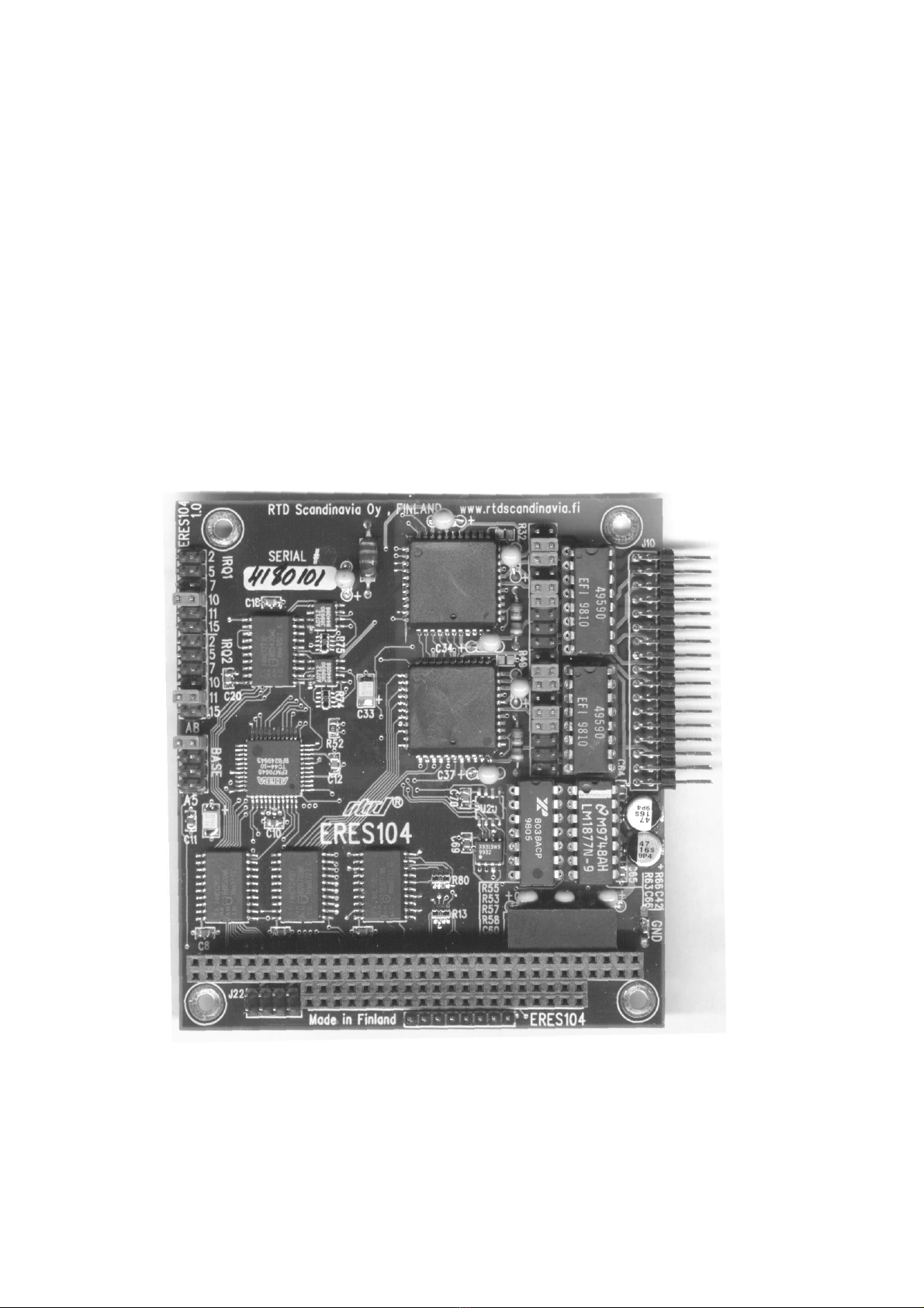
This user's manual describes the operation of the ERES104 2-channel PC/104
syncro/resolver subsystem.
Some of the key properties of the ERES104 include:
2 Independent Differential Syncro/Resolver/LVDT channels
Connection to 11.8V or 90V Syncros with onboard solid State Scott-T circuitry
Programmable sine wave excitation from 400Hz to 1.6KHz, global for both channels
Programmable resolution ranging from 10 to 16 bits
Error 8/4/2 minutes
Resolution 16-bits guaranteed with onboard reference source.
Fully PC/104 compliant
+5V only operation
The following paragraphs briefly describe the major features of the ERES104. A more
detailed discussion is included in Chapter 3 (Hardware description) The board settings are
described in Chapter 1 (Board settings).
Syncro/Resolver inputs
The ERES104 provides independently configurable input channels. Both
channels support Syncro, Resolver or LVDT interface. The voltage of the Syncro
inputs can be selected to either 11.8V or 90V standard devices. You may use the onboard
excitation oscillator or you may wish to use an external reference source. The external
reference signal is scalable with an onboard voltage divider. Reference phase shift can be
adjusted with a resistor capacitor pair for each channel (not factory set). Special design
procedures have been followed to ensure error free stable operation even up to 16-bit
resolution. Both input channels have independent grounds for reference and sensors. Syncro
signals are converted to sine/cosine resolver signals with a laser trimmed precision solid state
Scott-T converter. The resolver signal is then digitized by the onboard resolver-to-digital
converters.
Excitation circuitry
A programmable reference oscillator is available onboard to drive sensors.
The frequency and amplitude of the sine wave are programmable. Digital potentiometers
are used to give stable operation and flexible 32-step adjustment of excitation characteristics.
The reference source is common to both channels. Independent output buffer amplifiers
are used to drive the sensors. The onboard DC/DC converter can be used to drive total
loads of 1,5W. If you connect the bus power to drive the excitation amplifier circuitry you
may increase the drive to 2,5W. In this case make sure you provide adequate airflow around
the excitation amplifier not to thermally overload the device. The excitation frequency is
factory set to 400Hz to 1,6KHz range. This range can easily be increased to 2,6KHz to work
with common resolver types with a small adjustment. Please consult tha factory for more
details.
Page 2
ERES104 Ver 1.2 (c) RTD Finland Oy 2000-2001

Mechanical description
The ERES104 is designed on a PC/104 form factor. An easy mechanical interface to
both PC/104 and EUROCARD systems can be achieved. Stack your ERES104 directly on a
PC/104 compatible computer using the onboard mounting holes. Care must be taken to
ensure good quality cabling to ensure high quality noise free operation .
Connector description
The connections are made by header type terminals. RTD Finland may deliver
boards with or without headers. The PC/104 bus connector is 16-bit wide stackthrough type.
What comes with your board
You receive the following items in your ERES104 shipment:
* ERES104 PC/104 resolver to digital converter board
* User's manual
Note: DOS/WIN95/98/2000/NT 4.0 drivers and test software
are available from our website at www.rtdfinland.fi.
If any item is missing or damaged, please call Real Time Devices Finland
customer service department at (+358) 9 346 4538.
Scope of this manual
This manual expects the user to be familiar with syncros and resolvers. The theory
and operation or these sensors is not within the scope of this manual.
Using this manual
This manual is intended to help you install your new ERES104 module and get it
working quickly, while also providing enough detail about the board and it's functions so
that you can enjoy maximum use of it's features even in the most demanding applications.
When you need help
This manual and all the example programs will provide you with enough information
to fully utilize all the features on this board. If you have any problems installing or using this
board, contact our Technical Support Department (+358) 9 346 4538 during European
When sending a FAX or Email request, please include your company's name and address,
your name, your telephone number, and a brief description of the problem.
Page 3
ERES104 Ver 1.2 (c) RTD Finland Oy 2000-2001

CHAPTER 1 - BOARD SETTINGS
===============================================================
The ERES104 board has jumper settings to configure the operation of the board.
Special care must be taken to make correct connections since high voltage input signals
may be used.
Page 4
ERES104 Ver 1.2 (c) RTD Finland Oy 2000-2001

Factory configured jumper settings
Figure 1-1 illustrates the general location of the onboard connectors and
jumpers. Table 1-1 will show some general jumper settings preset by the factory.
Refer to the following jumper specific information on usage of these jumpers.
Jumper name Function Setting
BASE Base address 300h
IRQ1 Channel 1 IRQ 10
IRQ2 Channel 2 IRQ 11
SENSOR1 Sensor selection Direct resolver
SENSOR2 Sensor selection Direct resolver
Table 1-1 Factory preset jumpers
Fig. 1-1 Jumper and connector locations of the ERES104
Page 5
ERES104 Ver 1.2 (c) RTD Finland Oy 2000-2001

BASE - Base Address Jumpers (Factory setting: 300h)
The most common cause of failure when you are first setting up your module is
address contention. Some of your computers I/O space is already occupied by other
internal I/O devices and expansion boards. When the ERES104 attempts to use it's reserved
I/O addresses already used by another peripheral device erratic performance may occur
and data read from the board may be corrupted.
To avoid this problem make sure you set up the base address first using the five
jumpers which let you choose from 32 different I/O addresses in your computers I/O map.
Should the factory installed setting of 300h be unusable for your system configuration, you
may change this setting to another using the options illustrated in Table 1-2. The table shows
the switch settings and their corresponding values in hexadecimal values. Make sure you
verify the correct location of the base address jumpers. When the jumper is removed it
corresponds to a logical "0", connecting the jumper to a "1".
Base Address Jumper Settings ERES104
Hex / (Decimal) Jumper Settings Hex / (Decimal) Jumper Settings
Addr 5 6 7 8 Addr 5 6 7 8
200 / (512) 0 0 0 0 300 / (768) 0 0 0 1
220 / (544) 1 0 0 0 320 / (800) 1 0 0 1
240 / (576) 0 1 0 0 340 / (832) 0 1 0 1
260 / (592) 1 1 0 0 360 / (848) 1 1 0 1
280 / (512) 0 0 1 0 380 / (768) 0 0 1 1
2A0 / (544) 1 0 1 0 3A0 / (800) 1 0 1 1
2C0 / (576) 0 1 1 0 3C0 / (832) 0 1 1 1
2E0 / (592) 1 1 1 0 3E0 / (848) 1 1 1 1
Table 1-2 Base address jumpers
Note: The top-most jumper is equivalent to address line A8, the bottom-most is A5.
Fig. 1-2 Base address jumper showing base address 300H
Page 6
ERES104 Ver 1.2 (c) RTD Finland Oy 2000-2001

IRQ1/IRQ2 - Host Interrupt selection jumper (Factory settings: IRQ10/11)
The ERES104 can assert a host interrupt using the hardware interrupts IRQ
2,5,7,10,11,15. The selection of these interrupts is performed by closing one position on
the jumper header connector markes IRQ1 for channel 1 or alternatively IRQ2 for channel 2.
The interrupt header is illustrated below in figure 1-3.
Fig. 1-3 Host interrupts set to factory defaults
SENSOR1/2 - Sensor type selection jumpers
(Factory settings: straight resolver)
The sensor configuration jumper blocks consist of 3 parts A,B and C. The jumper
blocks are identical for channels 1 and 2 and are located on top of each other on the board.
Figure 1-4 illustrates the sensor input terminal block.
Fig. 1-4 Sensor configuration terminal block, C and B block pins are : 2 4
1 3
Page 7
ERES104 Ver 1.2 (c) RTD Finland Oy 2000-2001

The configuration is the following for these terminal blocks:
ABC
1) Differential resolver 3-4 OFF 1-2
2) Resolver/Inductosyn 5-6 OFF 1-2
1-2
7-8
3) Syncro 5-6 1-2 3-4
1-2 3-4
7-8
4) Differential syncro 5-6 1-2 3-4
3-4
5) LVDT 1-2 OFF OFF
7-8
9-10
CHAPTER 2 - BOARD INSTALLATION
===============================================================
The ERES104 Syncro/Resolver interface board is very easy to connect to your
industrial distributed control system. Direct interface to PC/104 systems is easily achieved.
This chapter tells you step-by-step how to install your ERES104 into your system.
After completing the installation use the diagnostic and test software to fully
verify that your board is working.
Page 8
ERES104 Ver 1.2 (c) RTD Finland Oy 2000-2001

Board Installation
Keep your board in its antistatic bag until you are ready to install it to your system!
When removing it from the bag, hold the board at the edges and do not touch the components
or connectors. Please handle the board in an antistatic environment and use a grounded
workbench for testing and handling of your hardware.
Before installing the board in your computer, check the jumper settings. Chapter 1
reviews the factory settings and how to change them. If you need to change any settings,
refer to the appropriate instructions in Chapter 1. Note that incompatible jumper settings
can result in unpredictable board operation and erratic response.
General installation guidelines:
1. Turn OFF the power to your computer
2. Touch the grounded metal housing of your computer to discharge any
antistatic buildup and then remove the board from its antistatic bag.
3. Hold the board by it's edges and install it in an enclosure or place it on the
table on an antistatic surface.
4. Connect the board to the sensors using the sensor header connector.
Make sure the polarity of the cable is correct.
Installation integrated with a PC/104 module stack:
* Secure the four PC/104 installation holes with standoffs.
* Connect the board to the sensors and other peripherals using the interface
header connectors.
Fig. 2-1 ERES104 integrated in a PC/104 dataModule stack
Page 9
ERES104 Ver 1.2 (c) RTD Finland Oy 2000-2001

Synchro/Resolver connector
The two sensor inputs are located in header connector J10 to the right side of
the board. Signals are connected as described below:
Pin# J10 Function Pin# J10 Function
1 *** REF_OSC1 2 GND
3 SIN1 4 CH1_AGND
5 COS1 6 CH1_AGND
7 EXT_REF1 8 CH1_AGND
9 REF_OSC2 10 GND
11 SIN2 12 CH2_GND
13 COS2 14 CH2_GND
15 EXT_REF2 16 CH2_GND
17 GND 18 GND
19* S1_1/S1_DR1 20 S3_1/S3_DR1
21 CH1_AGND 22** S4_DR1
23 S2_DR1 24 S2_1
25*** REF_OSC1 26*** REF_OSC2
27 S1_2/S1_DR2 28 S3_2/S3_DR2
29 CH2_AGND 30 S4_DR2
31 S2_DR2 32 S2_2
33 GND 34 GND
Table 2-1 Sensor interface connector J10 pinout
* S1 Channel 1 or differential resolver S1 channel 1
** Differential resolver S4
*** REF_OSC1 and REF_OSC2 are derived from the same source,
but buffered independently
/BIT led
A LED on the ERES104 indicated that either Channel #1 or Channel #2
Built-in-test error is active. If no error exists on either channel the LED is off. Note that if
you have only one sensor connected the LED is always lit since the other channel indicated
loss of signal error through it's built in test signal.
Page 10
ERES104 Ver 1.2 (c) RTD Finland Oy 2000-2001

Power connector
The power connector field illustrated in Figure 2-2 brings power to the ERES104
or it can be used to take power from the PC/104 stack.
Figure 2-2. Power connector of the ERES104.
Pin # J22 Description
1 GND
2 +5V
3 N.C.
4 +12V_BUS
5 -5V
6 -12V_BUS
7 GND
8 +5V
Table 2-2. Power connector of the ERES104.
Note 1. Pin #5 (-5V) is only connected to the PC/104 bus, it is not used
by the ERES104 board.
Note 2. -12V and +12V are connected to the PC/104 bus. These power
inputs are only used if the excitation source is powered from the
power connector. In this case the solder blobs on the solder side of
the board next to the power connector must be closed. (This mode is
usually set by the factory if the board setup requires this)
Note 3. The board is usually powered throgh the PC/104 host bus when not in
stand-alone mode. J22 can only used to power the module when power
is not available from the PC/104 bus.
Page 11
ERES104 Ver 1.2 (c) RTD Finland Oy 2000-2001

CHAPTER 3 - HARDWARE DESCRIPTION
===============================================================
This section describes the functionality of the vital subsections of the ERES104
board. These include the Resolver-to-Digital converters, Solid state Scott-T converter
and Sine wave excitation oscillator.
BELOW ARE LISTED THE EXTERNAL COMPONENT VALUES OF THE
RDC-19220 RESOLVER-TO-DIGITAL CONVERTER. FOR MORE INFORMATION
ON SELECTING THESE COMPONENTS, PLEASE REFER TO THE APPLICATION
NOTE DOCUMENTATION ON THE WEBSITE WWW.DDC-WEB.COM.
RC 30K
RS 53K
REF+ INPUT RESISTANCE 2K
RV 39K WITH 20K TRIMPOT (CENTERED) , EQ. 49K
CBW 4,7nF
RB 100K
CBW/10 470pF
Page 12
ERES104 Ver 1.2 (c) RTD Finland Oy 2000-2001

Resolver to Digital Converters
Two independent resolver-to-digital converters condition the sensor inputs.
These versatile chips have programmable resolution and internal diagnostic functions.
The control of these converters is performed by the host computer. These converters
support a variety of operational modes provided by the circuitry onboard, these include
Resolvers, Inductosyns, Syncros and LVDT's that can conditioned with up to 16-bit
resolution. The following passage will illustrate these connections.
Connecting Resolvers to ERES104
The figure 3-1a illustrates a generic resolver connection scheme to the converter.
Figure 3-1b shows a real connection that is used on the ERES104. The dashed line describes
the onboard precision resistor pack that is used to precondition the voltage range
of the sensors to a suitable level. If non differentially connected resolvers are used they
connect directly to the sin and cos inputs of the appropriate channels.
Figure 3-1a Differential resolver connection to a ERES104
Page 13
ERES104 Ver 1.2 (c) RTD Finland Oy 2000-2001

Figure 3-1b Differential resolver connection to ERES104
S1 is in pin #19, S3 is in pin #20, S4 is in pin #21, S2 is in pin #22 of J10
as an example for channel #1
S1 is in pin #27, S3 is in pin #28, S4 is in pin #30, S2 is in pin #31 of J10
as an example for channel #2
Connect A jumper 3-4; and C jumper 1-2
Connecting Inductosyns to ERES104
The ERES104 can also be used to interface to Inductosyn type scales. The Inducto-
syn scale output is very low, in the range of 2-10mV pp. The signal is identical to that of a
resolver. From the point of view of the RD-converter the Inductosyn signal must be
preamplified to the level of 2V rms that is required by the chips. This must be performed
by an external balanced preamplifier pair external to the ERES104. Please consult the factory
for hints on Inductosyn interfacing.
The onboard sine wave oscillator output current drive is limited. This means that it
willnot in many cases be sufficient to drive a low impedance Inductosyn slide that may have a
resistance in the magnitude of Ohms. RTD gan give hints on how to do this.
Page 14
ERES104 Ver 1.2 (c) RTD Finland Oy 2000-2001

Connecting Syncros to ERES104
The figure 3-2a illustrates a generic resolver connection scheme to the converter.
Figure 3-1b shows a real connection that is used on the ERES104. The dashed line describes
the onboard precision resistor pack that is used to precondition the voltage range of the
sensors to a suitable level of 2V.
Fig. 3-2a Generic Syncro connection to a Resolver-to-Digital converter
Fig. 3-2b Syncro connection to a ERES104
S1 is in pin #19, S3 is in pin #20, S2 is in pin #24 of J10
as an example for channel #1
S1 is in pin #27, S3 is in pin #28, S2 is in pin #32 of J10
as an example for channel #2
Connect B jumper 1-2,3-4 , A jumper 5-6; and C jumper 3-4
Page 15
ERES104 Ver 1.2 (c) RTD Finland Oy 2000-2001

Connecting LVDT's to ERES104
Standard 2-wire LVDT's interface to the Resover-to-Digital converters as
illustrated below. Please consult the factory in applications involving LVDT interfacing.
Fig. 3-3a Illustrates a generic 2-wire LVDT connection to a converter.
The prescision amplifier circuitry presented above is external to the ERES104.
Such LVDT preamplifier modules are availalable from RTD as standard products, or
they may be designed by RTD to suit customer specific requirements. Please contact
RTD for more information on different soultions for LVDT interfacing.
Page 16
ERES104 Ver 1.2 (c) RTD Finland Oy 2000-2001
Table of contents
Popular Recording Equipment manuals by other brands

Roger
Roger RUD-1 installation guide

INVADERS Amplification
INVADERS Amplification AmpsCabs owner's manual

Renishaw
Renishaw HSI-C quick start guide

Mitsubishi
Mitsubishi QJ71MT91 user manual

Bosch
Bosch FLM-420/4-CON-S installation guide

Lingg Janke
Lingg Janke KNX COMIP-REG-1 Operation and installtion manual