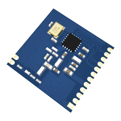
Realtek RTL8366 User manual

6/9-PORT 10/100/1000MBPS SWITCH CONTROLLER
and 10/100/1000 DUAL ETHERNET TRANSCEIVER
LAYOUT GUIDE
Rev. 1.1
29 August 2005
Track ID: JATR-1076-21
RTL8366/8369 &
RTL8212

RTL8366/8369 & RTL8212
Layout Guide
RTL8366/8369 & RTL8212 Layout Guide 2Track ID: JATR-1076-21 Rev. 1.1
COPYRIGHT
©2005 Realtek Semiconductor Corp. All rights reserved. No part of this document may be reproduced,
transmitted, transcribed, stored in a retrieval system, or translated into any language in any form or by any
means without the written permission of Realtek Semiconductor Corp.
TRADEMARKS
Realtek is a trademark of Realtek Semiconductor Corporation. Other names mentioned in this document
are trademarks/registered trademarks of their respective owners.
DISCLAIMER
Realtek provides this document “as is”, without warranty of any kind, neither expressed nor implied,
including, but not limited to, the particular purpose. Realtek may make improvements and/or changes in
this document or in the product described in this document at any time. This document could include
technical inaccuracies or typographical errors.
USING THIS DOCUMENT
Though every effort has been made to ensure that this document is current and accurate, more information
may have become available subsequent to the production of this guide. In that event, please contact your
Realtek representative for additional information that may help in the development process.
REVISION HISTORY
Revision Release Date Summary
1.0 2005/08/11 First release.
1.1 2005/08/29 Change all model numbers RTL8365 to RTL8366.
Add RREF and MDI_REF pin design rule (See section 2.1 General Guidelines, page 5).

RTL8366/8369 & RTL8212
Layout Guide
RTL8366/8369 & RTL8212 Layout Guide 3Track ID: JATR-1076-21 Rev. 1.1
Table of Contents
1. GENERAL DESCRIPTION................................................................................................................................................4
2. GENERAL DESIGN AND LAYOUT GUIDE ...................................................................................................................5
3. RSGMII PCB LAYOUT GUIDELINES ............................................................................................................................6
4. TRANSFORMER OPTIONS............................................................................................................................................12
List of Figures
FIGURE 1. LONG TRACE LAYOUT FOR RSGMII .............................................................................................................................6
FIGURE 2. TRACE WIDTH AND SPACING RECOMMENDATION FOR MICROSTRIP..............................................................................7
FIGURE 3. SYMMETRICAL ROUTING...............................................................................................................................................7
FIGURE 4. SYMMETRICAL ROUTING INTO AC CAPS.......................................................................................................................8
FIGURE 5. RSGMII LAYOUT REFERENCE ......................................................................................................................................8
FIGURE 6. MDI DIFFERENTIAL LAYOUT REFERENCE.....................................................................................................................9
FIGURE 7. SEPARATE SERDES GND AND SYSTEM GND VIA A BEAD............................................................................................10
FIGURE 8. RTL8212 COMPONENT SIDE FOOTPRINT ....................................................................................................................10
FIGURE 9. RTL8212 SOLDER SIDE FOOTPRINT............................................................................................................................10
FIGURE 10. UTP APPLICATION CIRCUIT WITH TRANSFORMER.......................................................................................................12

RTL8366/8369 & RTL8212
Layout Guide
RTL8366/8369 & RTL8212 Layout Guide 4Track ID: JATR-1076-21 Rev. 1.1
1. General Description
This document provides detailed design and layout guidelines to achieve the best performance when
implementing a 4-layer board design with the RTL8366/8369 10/100/1000Mbps switch controller, and
the RTL8212 dual port 10/100/1000Mbps Ethernet transceiver.
The RTL8366 and RTL8369 are 128-pin, ultra-low-power, high-performance 5/8-port Gigabit Ethernet
switches, with one extra GMII/MII/RGMII port for specific applications. They integrate all the functions
of a high speed switch system; including SRAM for packet buffering, non-blocking switch fabric, internal
register management, and an embedded 8051 into a single 0.15µm CMOS device. Only a 25MHz crystal
is required; an optional EEPROM is offered for internal register configuration.
The 6/9th port of the RTL8366/8369 implements a GMII/MII/RGMII interface for connecting with an
external PHY or MAC in specific applications. This interface could be connected to an external CPU or
RISC in 1 WAN + 4 LAN or 1 WAN + 8 LAN Router applications.
The RTL8212 integrates dual independent Gigabit Ethernet transceivers into a single 0.13µm CMOS
device and includes the PCS, PMA, and PMD sub-layers. They perform encoding/decoding, clock/data
recovery, digital adaptive equalization, echo cancellers, cross-talk elimination, line driver, as well as all
other required support circuit functions.

RTL8366/8369 & RTL8212
Layout Guide
RTL8366/8369 & RTL8212 Layout Guide 5Track ID: JATR-1076-21 Rev. 1.1
2. General Design and Layout
In order to achieve maximum performance with the RTL8366/8369 and RTL8212, good design attention
is required throughout the design and layout process. The following recommendations will help
implement a high performance system.
2.1. General Guidelines
•Provide a good power source, minimizing noise from switching power supply circuits (<100mV).
•Verify the critical components, such as clock source and transformer, to meet the application
requirements.
•Keep power and ground noise levels below 100mV.
•Use bulk capacitors (4.7uF-10uF) between each power and ground plane.
•Use 0.1uF decoupling capacitors to reduce high-frequency noise on the power and ground planes.
•Keep decoupling capacitors as close as possible to the RTL8366/8369 and RTL8212.
•Fill in unused areas of component side and solder side with solid copper and attach them with
vias to ground plane.
•The RREF pin of the RTL8366/8369 and the MDI_REF pin of the RTL8212 must connect to
GND via a 2.49K +/- 1% Ohm resister. This resister must be placed as close as possible to the
RTL8366/8369 and RTL8212.

RTL8366/8369 & RTL8212
Layout Guide
RTL8366/8369 & RTL8212 Layout Guide 6Track ID: JATR-1076-21 Rev. 1.1
3. RSGMII PCB Layout Guidelines
As the RSGMII transmits over 2.5GHz differential signal pairs, the PCB layout needs some attention in
order to meet layout guidelines. The following lists some important guidelines for layout of the RSGMII
in a 4-layer PCB.
•Differential impedance is 100Ω±10% and single-ended impedance is 60Ω±6%.
•All micro-strip traces of a differential pair should be 5-mil-wide with 7-mil-wide air-gap spacing
between the traces of the pair.
•Spacing to all non-Serdes signals should be at least 30-mil in order to avoid harmful coupling
issues.
•Trace routes over long distances should be routed at an off-angle to the X-Y axis of a PCB layer
to distribute the effects of fiberglass bundle weaves and resin-rich areas of the dielectric. See
Figure 1 for an illustration of diagonal routing.
Resin-ri ch A reas
of Di el ectri c
Fiberglass Bundles
of Dielectri c
Preferred Di f ferenti al
Pair Routing for
LongLengths
A voi d thi s T ype of
Routi ng f or L ong
Lengths
Figure 1. Long Trace Layout for RSGMII

RTL8366/8369 & RTL8212
Layout Guide
RTL8366/8369 & RTL8212 Layout Guide 7Track ID: JATR-1076-21 Rev. 1.1
TX Pair 25M CLK RX Pair
5 mi l s
5 mils
7 mils
5 mils
5 mils
7 mils
>=30 mils >=30 mils
Figure 2. Trace Width and Spacing Recommendation for Microstrip
•Differential pairs should maintain symmetry between the two signals of a differential pair
whenever possible.
Preferred: Symmetri cal Routi ng
A voi d: Non-symmetri cal Routi ng
Figure 3. Symmetrical Routing
•Keep differential pair routing lengths as short as possible.
•Match the length of both sets of the differential pairs, allowing no more than a 5-mil delta
between the lengths of the two signals.
•Length matching should occur on a segment-by-segment basis vs. across the total distance of the
overall route.
•Differential pairs should have a continuous reference plane, and avoid vias.
•Size 0402 AC coupling capacitors are strongly encouraged as the smaller the package size, the
less ESL.
•Place AC coupling capacitors near output pins of differential pairs.
•Locate capacitors for coupled traces at the same location along the differential traces and near
output pins of differential pairs.

RTL8366/8369 & RTL8212
Layout Guide
RTL8366/8369 & RTL8212 Layout Guide 8Track ID: JATR-1076-21 Rev. 1.1
A C C ap Pads
Preferred
(Cap placement is in same location & symmetric)
Avoid
(Cap placement is not in same location & symmetric)
Figure 4. Symmetrical Routing Into AC Caps
•RSGMII layout reference is shown in Figure 5.
Figure 5. RSGMII Layout Reference

RTL8366/8369 & RTL8212
Layout Guide
RTL8366/8369 & RTL8212 Layout Guide 9Track ID: JATR-1076-21 Rev. 1.1
3.1. Ethernet MDI Differential Signals
•Keep differential-pair impedance at 100Ω±10%, single-ended impedance at 60Ω±6%.
•All microstrip traces of a differential pair should be 5-mil wide with a 7-mil wide air gap spacing
between the trace of the pair.
•Keep differential pairs as close as possible and route both traces as identically as possible,
meaning width, length, and location.
•Avoid vias and layer change if possible.
•MDI Differential layout reference is show in Figure 6.
Figure 6. MDI Differential Layout Reference

RTL8366/8369 & RTL8212
Layout Guide
RTL8366/8369 & RTL8212 Layout Guide 10 Track ID: JATR-1076-21 Rev. 1.1
3.2. RTL8212 Layout Note
•Separate Serdes ground (AVSS pin46, pin48) and system ground by a bead (size= 0603).
See Figure 7.
AVSS
Pin 48 Pin 46
.
RT L 8212
QFN76
Bead
Figure 7. Separate Serdes GND and System GND via a Bead
•Use multi-vias (drill size= 20~24 mil) in the RTL8212 footprint and fill in large areas of
component side and solder side with solid copper. Then attach them with vias to the ground plane
in order to reduce the temperature of the PCB.
•The following figures are examples of an RTL8212 footprint.
Figure 8. RTL8212 Component Side Footprint
Figure 9. RTL8212 Solder Side Footprint

RTL8366/8369 & RTL8212
Layout Guide
RTL8366/8369 & RTL8212 Layout Guide 11 Track ID: JATR-1076-21 Rev. 1.1
3.3. Clock Circuit
•Place the crystal as close to the RTL8366/8369 as possible.
•Surround the clock with ground trace to minimize high-frequency emissions.
•Use only one 1.5K pull up external resistance to 3.3V for MDIO.
•Keep the MDC trace away from the other signals, to avoid unnecessary interference.
•Keep clearance area under the crystal or OSC component.
•Don’t let the clock trace pass over a gap in the ground plane.
3.4. Power Planes
•When designing a 4-layer PCB layout, divide the power plane into 3.3V_MAC, 3.3V_PHY, 1.8V
and 1.2V.
•Use 0.1µF decoupling capacitors and bulk capacitors between each power plane and ground plane.
3.5. Ground Planes
•Keep the system ground region as one continuous, unbroken plane that extends from the primary
side of the transformer to the rest of the board.
•Place a moat (gap) between the system ground and chassis ground.
•Ensure the chassis ground area is voided at some point such that no ground loop exists on the
chassis ground area.

RTL8366/8369 & RTL8212
Layout Guide
RTL8366/8369 & RTL8212 Layout Guide 12 Track ID: JATR-1076-21 Rev. 1.1
4. Transformer Options
•The RTL8212 uses a transformer with a 1:1 turn ratio. There are many venders offering
transformer designs that meet the RTL8212’s requirement. Examples are Pulse H5014, Bothhand
GS5014, and Lankom LG4803S.
•A 10/100/1000Base-T UTP application circuit with transformer is show in Figure 10.
.
.
.
.
..
.
.
.
.
..
.
.
.
.
..
.
.
.
.
..
.
.
.
1
2
3
4
5
6
7
8
RJ45
RT L 8212
MDIDN
MDIDP
MDICN
MDICP
MDIBN
MDIBP
MDIAN
MDIAP
0.1uF
0.1uF
0.1uF
0.1uF
75 ohm
75 ohm
75 ohm
75 ohm
1000pF/2K V
Figure 10. UTP Application Circuit with Transformer
Realtek Semiconductor Corp.
Headquarters
No. 2, Industry East Road IX, Science-based
Industrial Park, Hsinchu, 300, Taiwan, R.O.C.
Tel: 886-3-5780211 Fax: 886-3-5776047
www.realtek.com.tw
This manual suits for next models
2
Table of contents
Other Realtek Wireless Module manuals
Popular Wireless Module manuals by other brands

ESD
ESD CAN-CBX-REL4 manual

Telit Wireless Solutions
Telit Wireless Solutions BlueMod+S50 HW User Guide

AzureWave
AzureWave AW-CU288 manual

Telit Wireless Solutions
Telit Wireless Solutions ME310G1 HW Design Guide

GEZE
GEZE 163051 Supplementary sheet

Universal Electronics
Universal Electronics 590070000006 Quick reference guide