Document Number: UM0058
_______________________________________________________________
March 8, 2016 2
Table of Contents
1Hardware block diagram......................................................................................................... 3
2System requirements .............................................................................................................. 4
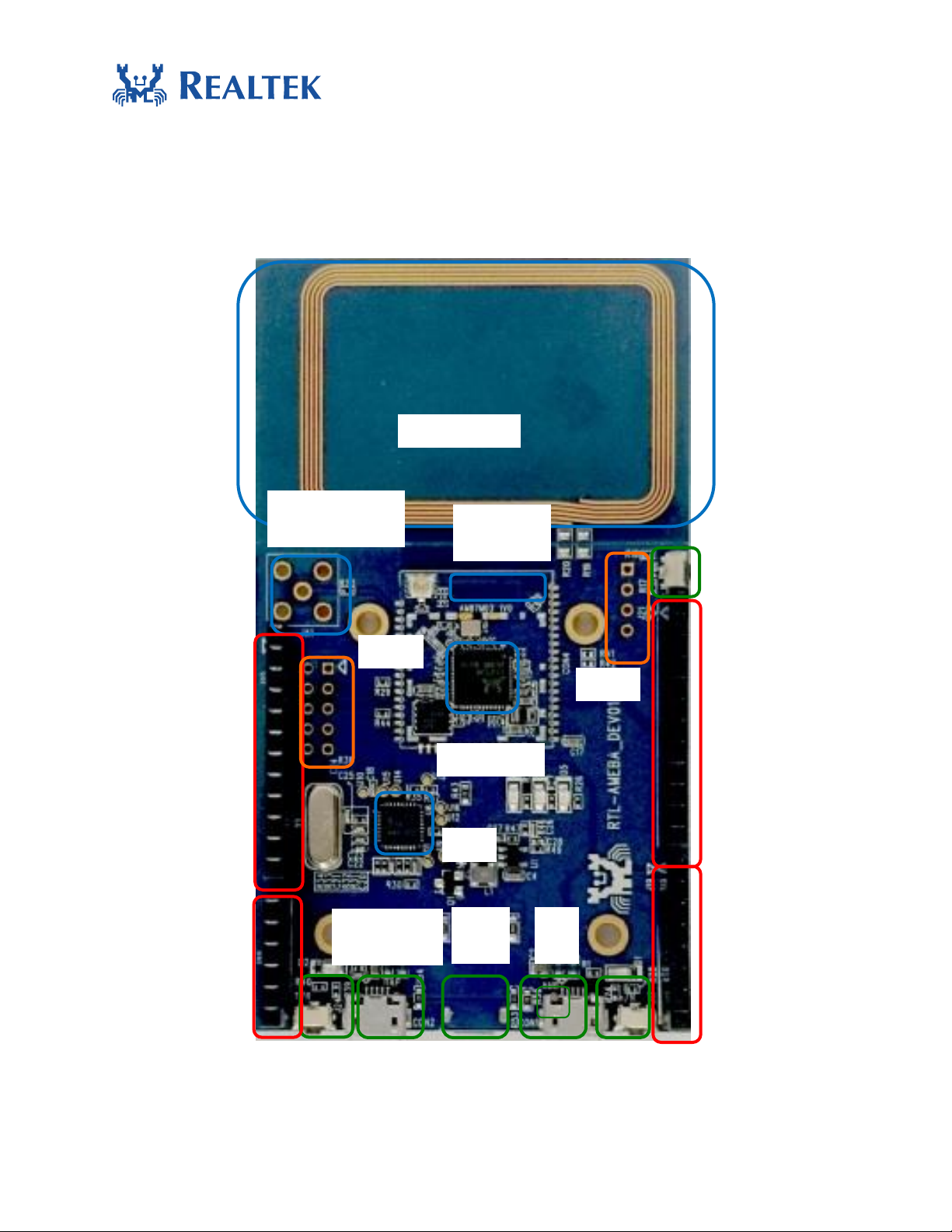
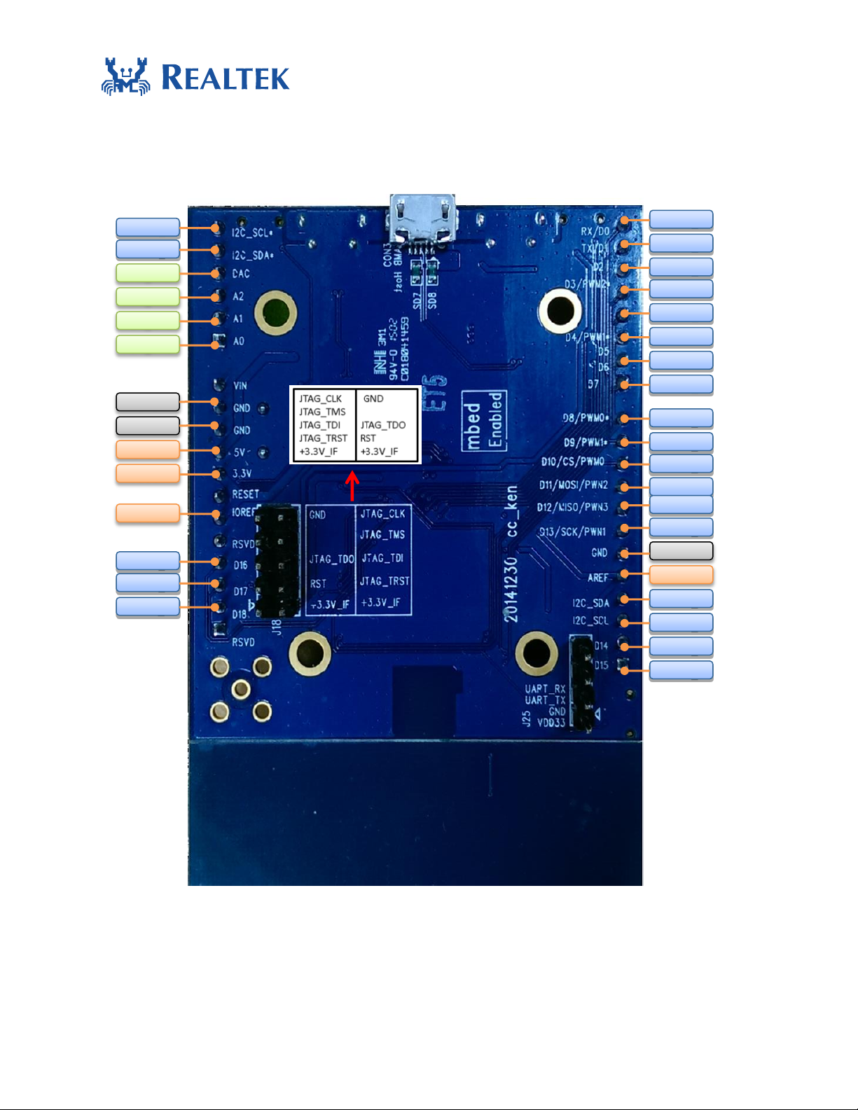
3Pin out reference..................................................................................................................... 4
3.1 Pin out table.................................................................................................................... 4
3.2 Pin out reference ............................................................................................................ 5
3.3 Pin connection table ...................................................................................................... 6
4Antenna hardware setup ........................................................................................................ 7
5Peripherals support................................................................................................................. 7
5.1 Pin function table setup.................................................................................................. 8
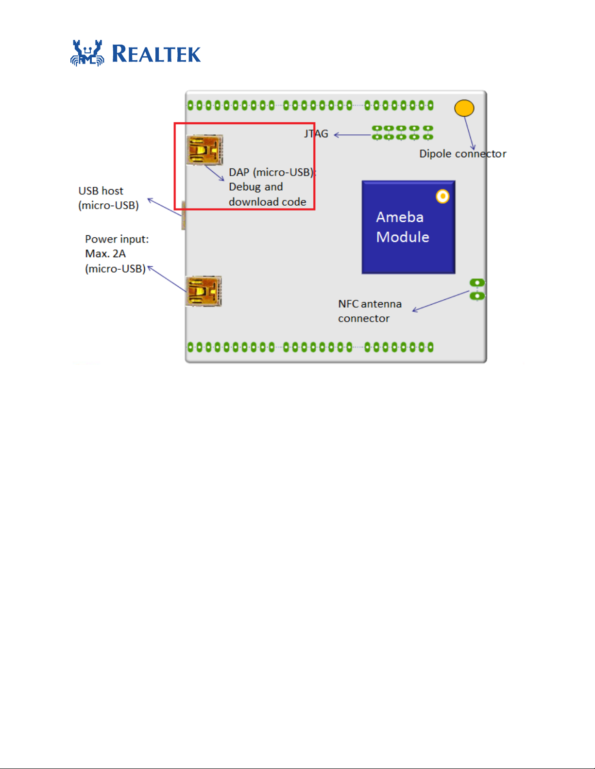
6Hardware configuration .......................................................................................................... 8
6.1 CMSIS-DAP ...................................................................................................................... 8
6.2 J-Link/JTAG...................................................................................................................... 9
6.3 DAP mode ..................................................................................................................... 11
7Ameba1 DEV01 pin out......................................................................................................... 13
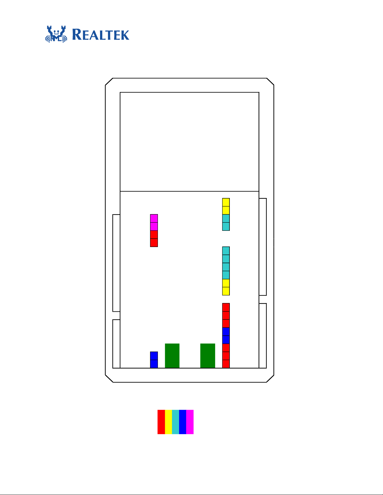
8Sensor board ......................................................................................................................... 14
9Warning................................................................................................................................. 15
10.1 Federal Communication Commission Interference Statement ....................................... 15
10.2 Industry Canada Statement ......................................................................................... 17
10.3 NCC 警語....................................................................................................................... 20
10.4 Japan Statement ............................................................................................................... 20