R16AN0002EU0300 Rev.3.00 Page 9
Jan 6, 2022
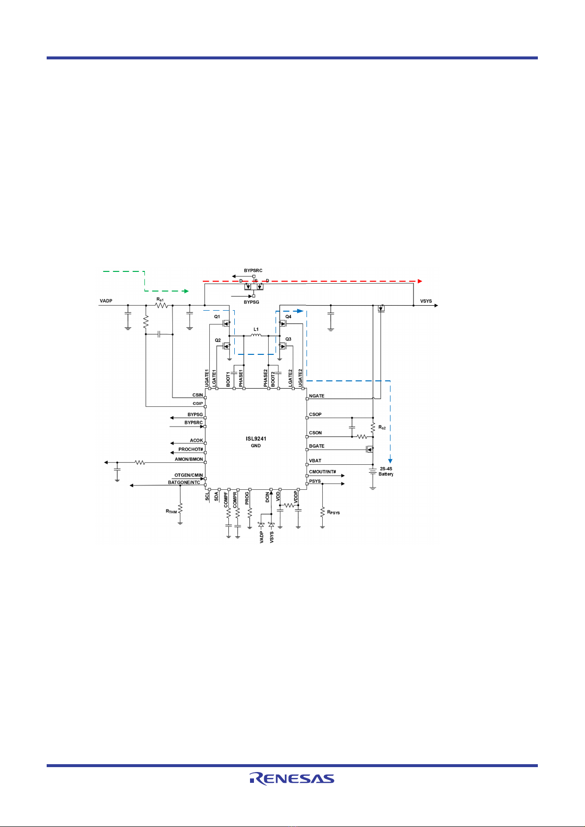
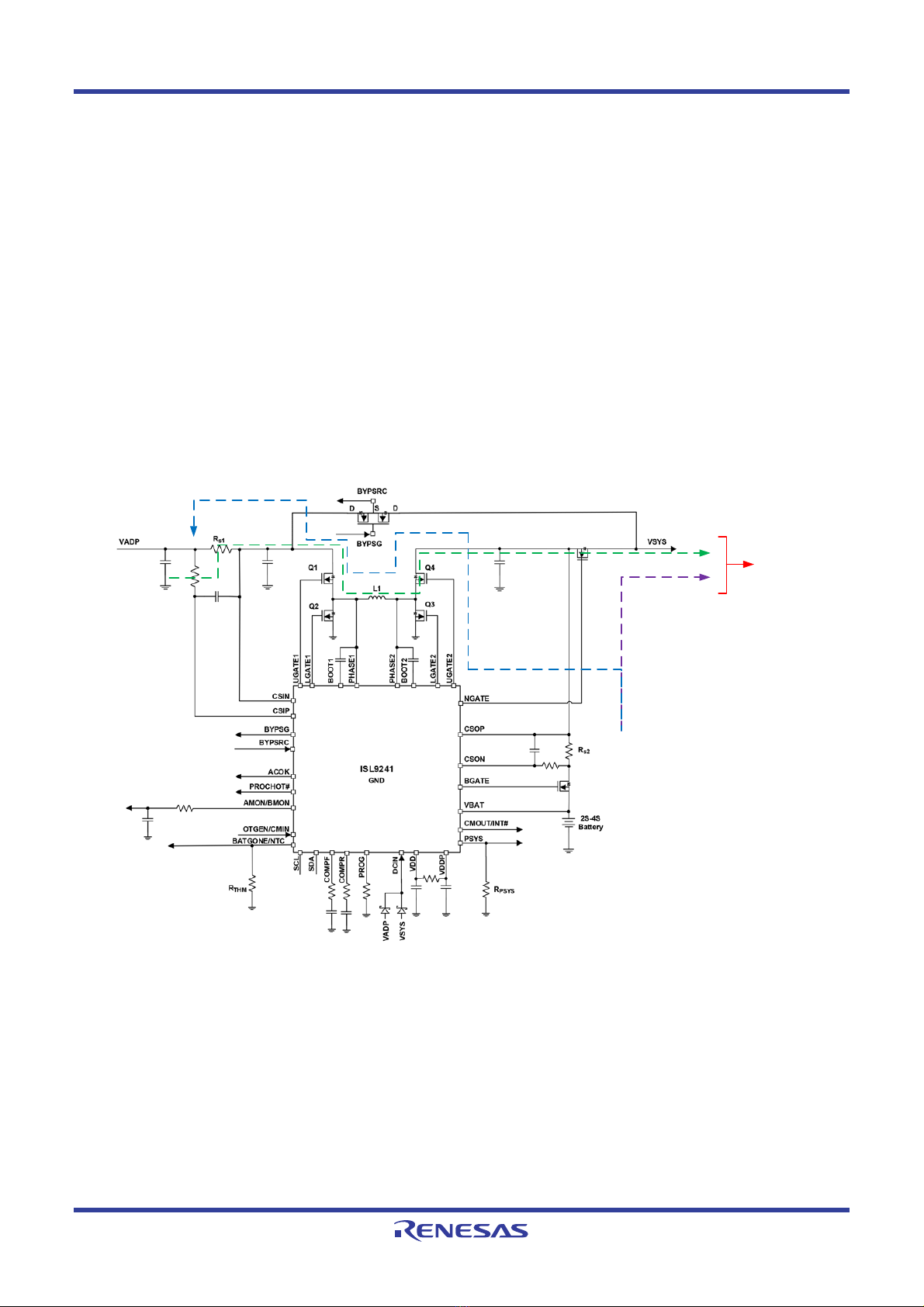
ISL9241 Operation Modes Application Note
Suggestions:
▪If the adapter is removed at any time and ACOK goes low during Steps 1 to 3, stop executing the commands
and complete steps for Bypass to BAT state.
▪If the adapter is removed after Step 4, complete all steps and then execute the commands for Bypass to BAT.
▪If the adapter is removed after completing all steps, first transition to Bypass state (from Bypass+Charging or
Reverse Turbo Boost) and then transition to BAT state.
▪CV mode regulation is not recommended in Bypass mode without Charging or Reverse Turbo boost. So enable
charging and Reverse Turbo Boost along with setting MaxsysV to non-zero value.
▪NGATE FET and Bypass FET power good signals can be read from the Information 1 register (0x3A) to ensure
that there is no unexpected behavior in the system.
▪Enable slew rate if output caps are high and inrush can be high to prevent protection from tripping. Capacitor
can be added on Bypass gate if inrush during turn on needs to be limited.
2.2 Transitioning from Bypass to NVDC or NVDC + CHRG
Note: To transition from Bypass mode to NVDC, turn off charging and RTB mode first. The system load must be
reduced so that the system current never exceeds the ISL9241 Adapter Current Limit value.
After turning off the battery FET, the ISL9241 output is ramped up to the adapter voltage. The NGATE FET is
closed, connecting the output of the ISL9241 to the system. The Bypass FETs then open, isolating the adapter
and the system output. The ISL9241 output and system are ramped down close to the battery voltage so that
charging can be enabled safely any time. The system is regulated close to the battery voltage at the value
programmed in the MaxSystemVoltage register. Complete the steps in Tabl e 2 to transition from Bypass mode to
NVDC mode or NVDC + Charge mode.
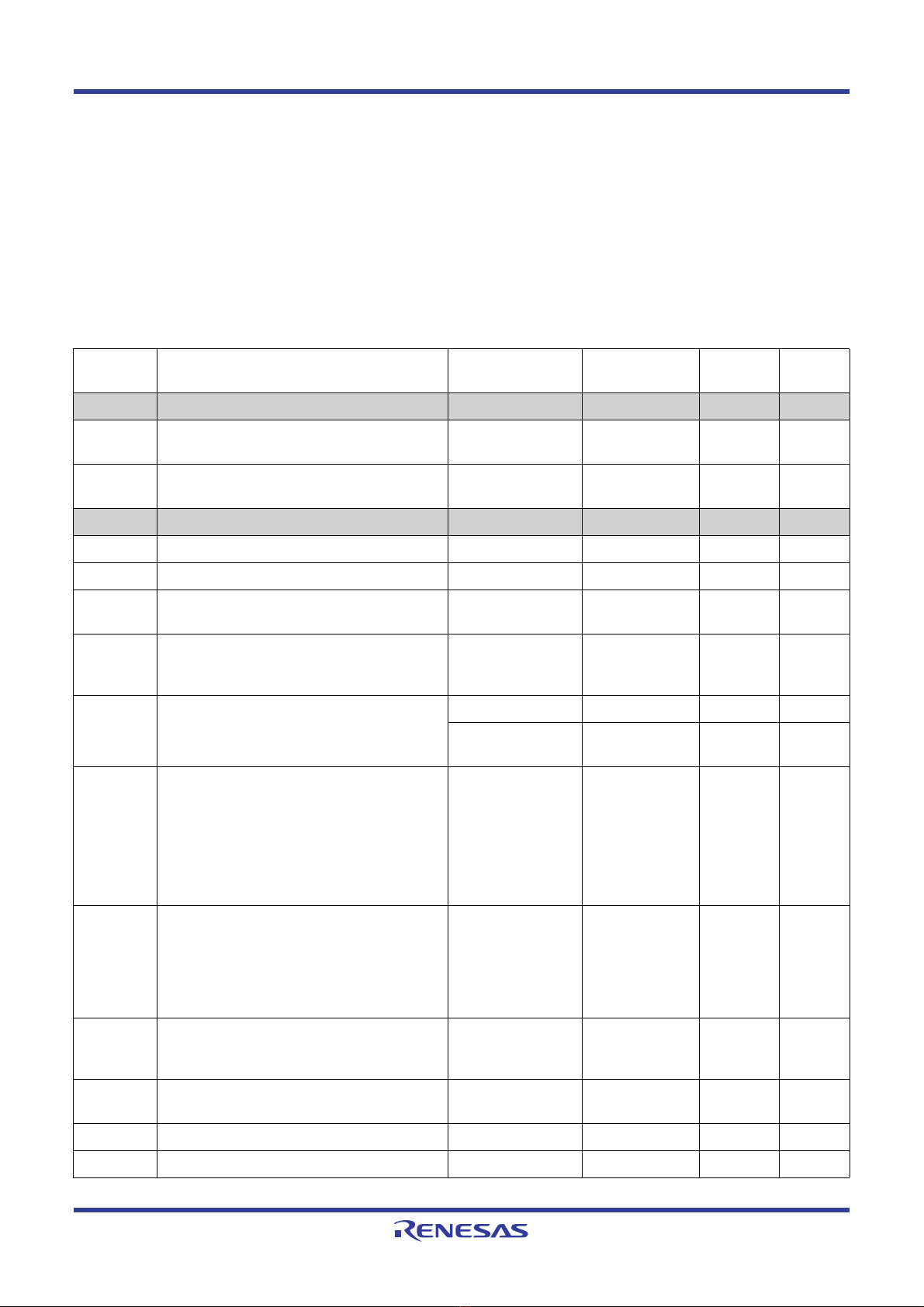
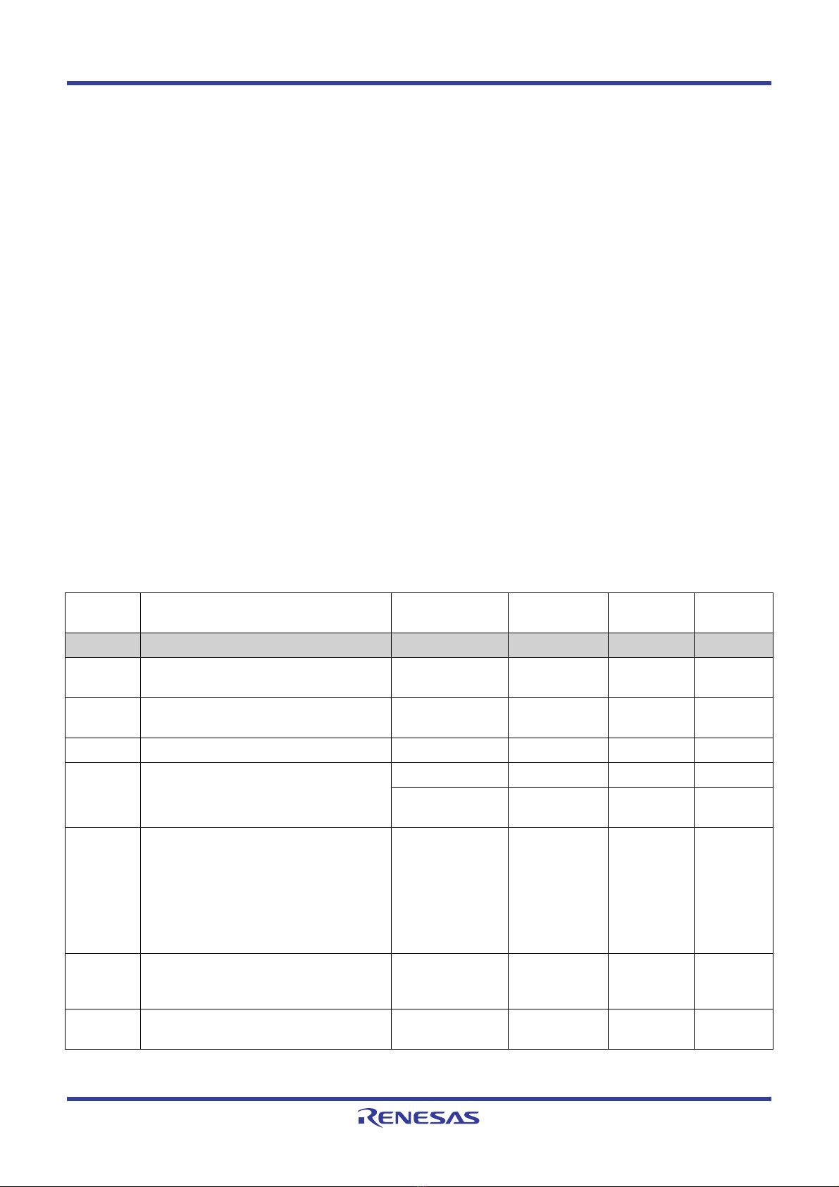
Table 2. Transitioning from Bypass Mode to NVDC (or NVDC + CHRG) Mode
Step
Number Function Description Register Name
Value
(Decimal) Read/ Write
Register
Address
BBypass to NVDC
Preparatio
n
Reduce system load below ACLIM
1 Disable Force Forward Buck/ Reverse Boost
mode
Control 4<10> 0 Write 0x4E
2 Turn off VIN/VOUT comparator Control 0<5> 0 Write 0x39
3 Set MaxSysVoltage = VADP (from ADC or
PD controller) - 2V
For 20V adapter, set 18.304V
Vin ADC register Read 0x87
MaxSysVoltage
register
Vin ADC
register - 2V
Write 0x15
Three options:
▪Wait fixed time (see Calculating Wait Time
to calculate wait time)
▪Wait fixed time and read ADC to confirm
VSYS = MaxSysVoltage register
▪Poll ADC and check when
VSYS = MaxsysV register
4 Turn off Bypass gate, turn on NGATE, set
charge pumps to 100%, Enable 10mA
current source
Control 0 Hex 2040 Write 0x39
5 Set MaxSysVoltage = Battery full charge
voltage after 1ms
MaxSysVoltage
register
Battery specific Write 0x15