Sanyo RB-7201 User manual

FILE NO.
Service Manual
CONTENTS
DVD Video Player DVD-7201
PRODUCT CODE No.
137 103 01 (CA)
137 103 02 (UK)
137 103 03 (XE)
137 103 04 (AU)
137 103 05 (SS)
REFERENCE No. SM5810203
z/ON
STANDBY
Specifications...................................................................1
Laser beam safety precaution..........................................1
DVD Mechanism replacement .........................................2
Mechanism replacement..................................................3
Mechanism operation.......................................................4
DVD P.W.Board operation ...............................................5
DVD start-up program flow chart .....................................28
MPEG AND FRONT END
P.W.Board operation (block diagram) ............................30
MPEG P.W.Board (schematic diagram for wave check) .32
AMP P.W.Board (schematic diagram fir wave check) .....34
MPEG AND FRONT P.W.Board check waveform ...........36
How to load software for MPEG P.W.Board ....................41
Trouble shooting ..............................................................42
Voltage of IC and Transistor ............................................45
Exploded view (cabinet and chassis)...............................49
Parts list ...........................................................................50
Exploded view (DVD mechanism) ...................................54
Parts list ...........................................................................54
IC block diagram and description.....................................55
Schematic diagram (MPEG for AU, SS and CA) .............64
Schematic diagram (MPEG for XE and UK) ....................66
Wiring diagram (MPEG A SIDE) ......................................68
Wiring diagram (MPEG B SIDE) ......................................70
Schematic diagram (MAIN for AU and SS)......................72
Wiring diagram
(DG,SOCKET and POWER SW for AU and SS) ..........74
Wiring diagram (FRONT for XE and UK) .........................76
Schematic diagram (MAIN for AU and SS)......................78
Wiring diagram
(DG,SOCKET and POWER SW for XE and UK) ..........80
Wiring diagram (FRONT for XE and UK) .........................82
Schematic diagram (MAIN for CA)...................................84
Wiring diagram
(DG,SOCKET and POWER SW for CA) .......................86
Wiring diagram (FRONT for CA) ......................................88
Schematic diagram (DVD) ...............................................90
Wiring diagram (DVD A SIDE) .........................................100
Wiring diagram (DVD B SIDE) .........................................101
WIRING CONNECTION..................................................102
(XE)
REMOTE CONTROLLER RB-7201
z/ON
SETUP MENU
SUBTITLE
AUDIO TITLE RETURN
ON SCREEN LAST MEMOZOOM
SURROUND REPEAT A-B REPEAT
PROGRAMANGLE
SEARCH
MODE
MULTI-
VISION
PICTURE
MODE
ANGLE
REPLAY
NEXTPREV
FWD SLOWREV SLOW
PAUSE/STEP
PLAY
REV FWD
CLEAR
123C
456
7890
+10
4
b
5
a
ENT
(UK)
(AU)
(SS)
(CA)

- 1 -
Playback system ..................... DVD-Video , Video CD , CD
Playback standard .................. NTSC or PAL (CA : NTSC only)
Laser ....................................... Semiconductor laser,
wavelength 650nm
Laser output
(Continous wave max.) :
1 mW(DVD) , 0.5 mW(CD)
Frequency range ..................... 4 Hz to 44 kHz(DVD fs : 96kHz)
Signal to noise ratio ................ More than 105 dB
Harmonic distortion ................. 0.003 %
Wow and flutter ....................... Below measurable level
Output:
DIGITAL OUTPUT :
For optical cable
A/V EURO CONNECTOR :
For Euro-AV cable (UK,XE)
COMPONENT VIDEO OUT (CA)
Y.............................................1.0 Vp-p (75 ohm)
CB, CR....................................0.7 Vp-p (75 ohm)
S-VIDEO OUT
Y.............................................1.0 Vp-p (75 ohm)
C.............................................0.286 Vp-p (75 ohm) (NTSC)
0.3 Vp-p (75 ohm) (PAL)
(Except CA)
VIDEO OUT .................................1.0 Vp-p (75 ohm)
SPECIFICATIONS
AUDIO OUT .................................L, R : 2.0 V rms
Power requirements .....................AC 230 V, 50 Hz (XE,UK)
230 - 240 V 50 Hz (AU)
110 - 240 V 50/60 Hz (SS)
120 V, 60 Hz (CA)
Power consumption .....................14.5 Watts
Dimensions (W x H x D)...............Approx. 360 x 79 x 281 mm
Weight ..........................................Approx. 2.7 Kg
Specifications subject to change without notice.
LASER BEAM SAFETY PRECAUTION
DIGITAL
OUT
OPT.
RL
VIDEO OUT
AUDIO OUT
S-VIDEO OUT
TV SYSTEM
PAL NTSC AV EURO CONNECTOR
(RGB OUT)
VIDEO OUT SELECT
SRGB
CAUTION – INVISIBLE LASER RADIATION WHEN OPEN AND
INTERLOCKS DEFEATED. AVOID EXPOSURE TO BEAM.
ADVARSEL – USYNLIG LASER STRÅLING VED ÅBNING, NÅR
SIKKERHEDSAFBRYDERE ER UDE AF FUNKTION, UNDGÅ UDS ÆTTELSE
FOR STRÅLING.
VARNING – OSYNLIG LASER STRÅLNING NÄR DENNA DEL ÄR ÖPPNAD
OCH SPÄRR ÄR URKOPPLAD. STRÅLEN ÄR FARLIG.
VORSICHT – UNSICHTBARE LASERSTRAHLUNG TRITT AUS, WENN
DECKEL GEÖFFNET UND WENN SICHERHEITSVERRIEGELUNG
ÜBERBRÜCKT IST. NICHT, DEM STRAHL AUSSETZEN.
VARO – AVATTAESSA JA SUOJALUKITUS OHITETTAESSA OLET ALTTIINA
NÄKYMÄTTÖMÄLLE LASERSÄTEILYLLE. ÄLÄ KATSO SÄTEESEEN.
DIGITAL
OUT
OPT.
RL
VIDEO OUT
AUDIO OUT
S-VIDEO OUT
TV SYSTEM
PAL NTSC
(XE,UK)
(AU,SS)

- 2 -
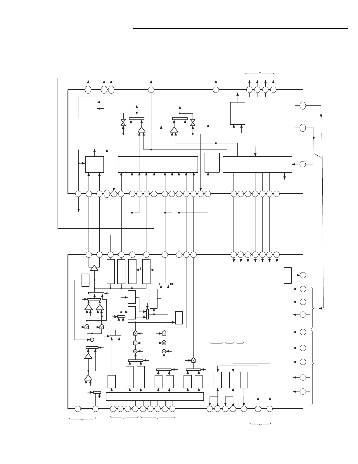
DVD MECHANISM REPLACEMENT
1.Cautionary instructions in handling the assy
(Safety instructions)
Optical pickup
The laser beam used in the pickup is classified as "class 2". Exposing
your eyes or skin to the beam is harmful. Take care not to do so.
(Caution against static electricity and leakage voltage)
Ground securely the work tables, tools, fixtures, soldering irons
(including those made of ceramic) and measuring instruments used
in the production lines and inspection departments that handle
loaders. The workers shall also be grounded.
(Cautionary instructions in handling)
Do not touch the object lens when handling a loader, or the lens will
be stained, resulting in inadequate playability.
There is no power supply protection circuit provided for this product
or adjustment/inspection device. Short-circuiting may lead to fire or
damage.
Take care so as to protect from exposure to water, the entry of
metallic pieces or dew condensation.
In particular, a strong magnet adjacent to the pickup will not only
get inoperative but can damage the pickup if a small metallic piece,
such as a screw or swarm, enters.
The loader edge can cause injury if inadvertently handled.
Do not touch a rotating disk, or injury may result.
This product is a precision device. Handle carefully.
A shock or dropping will cause misalignment or destruction. If it
should occur, refer to clause 2.
This product is so designed as to endure an initial shock equivalent
to a drop from a height of approx. 90 cm under the packed condition.
After the initial shock, the resistivity will still remain at a level of 50
to 60 G, but the mechanical robustness will weaken.
Do not place in a dusty location.
The entry and deposition of dirt into or on the pickup lens or moving
section will cause malfunction or degradation.
(Connectors)
Do not connect or disconnect while power is on.
Connecting or disconnecting signal wires or the main power cord
when the power is on may destruct the unit or fixture.
When connecting, push all the way in securely.
An insufficient insertion may cause a bad contact, leading to an
erroneous operation.
Do not connect or disconnect roughly by an excessively strong force,
or a broken wire or bad contact may result.
Semiconductors are connected. Do not touch connector terminals
directly.
If the worker is grounded, there is nothing to worry about static
electricity, but the rust on the connector terminal surface caused by
the touch may result in bad contact.
(Power source)
The power source need be good in quality (free from instantaneous
interruptions or noises).
A low quality power source may well cause malfunction.
(Storage)
Do not place or store in a dusty place or a place where dew
condensation is possible.
The entry and deposition of dirt or dust into or on the pickup lens or
moving section will cause malfunction or degradation.
Also, dew condensation causes rust;the rust penetrate into the
precision part of a pickup, causing malfunction, or degrading the
optical quality of the internal lens and reflector, which also leads to
malfunction.

- 3 -
MECHANISM REPLACEMENT
FLOIL OIL
G-474B
FLOIL OIL
G-2000B
FLOIL OIL
G-2000B
MOLYKOTE
EM-50L
MOLYKOTE
EM-50L
MOLYKOTE
EM-50L
MOLYKOTE
EM-50L
SILICON GREASE
KS-64
3. TRAY PART
MOLYKOTE
EM-50L
GREASE
CDF-409
GREASE
CDF-409
4. BASE MECHANISM PART
1. TRAY AND BASE MECHANISM PART
2. Base mechanism mounting PART
Do not remove the pick-up from base mechanism because of
adjustment difficulty.

- 4 -
MECHANISM OPERATION 3. Match the mark of GEAR 2and mark of GEAR 3 ,
and then install the BOSS.
4. Turn the GEAR 1counterclockwise, and then SLIDE
move right side.
5. The GEAR 1 move from side to side.
LOARDING
GEAR
MARKER
MARKER
TRAY
HOLE
6
7
8
9
1.How to setting the tray.
1. Move the SLIDE left side.
2. Match the Hole of GEAR 5 and Hole of CHASSIS 4 .
6. Match the hole of GEAR 7 and hole of chassis while turning
GEAR 6 .
7. Match the mark of LOADING GEAR 8 and gear of TRAY
where see horn hole 9 of tray.
8. Push a tray with the state that turned the entire surface of a
tray into approximately 5 degrees the lower part slowly.
CHASSIS
FRONT SIDE
MOTOR
MARKER
MARKER
1
2
2
3
3
RIB
RIB
GREASE
EM-50L
GREASE
EM-50L
GREASE
EM-50L
LARGE TOOTH
GEAR HOLE
CHASSIS HOLE
5
4

- 5 -
1. General operation diagram (This is a basic general operation diagram)
IC101
BU4066
IC100
LA9702 IC200
LC78661W
IC550
LE28C1001
IC502
M51953
IC500
M37903S4CHP
IC201
T224162B
IC900
BA033
CN900CN200CN500
IC504
TC7SHU04FU
REGULATOR
9V
(actuator)
(motor)
5V
(analog)
5Vd
(digital)
3.3V
(FOR DSP)
16.934MHZ
DSPJVAD
EMPH,C2F,LRCK,BCK,CD_DATA,SPDIF
SDT[O;7]
DCLK,DBGN,DERR
DREQ
DACK
16MHZ
INVERTER
PH 6P
FFC 26P
FFC 16P
FLASH MEMORY
RXD,SCLK
HD_INT,TXD,RDY_HIF
RESET
RESET HRST
16MHZ
DRAM
JV
BH
DEFECTI
RF AMP
RFOP,RFON,PH,TE,ADBH
ADBH
TOST,FOST,BST,VCA
TBAL,FBAL,SGC
DEF
DEFECTO
XHTR
FE
DEF_INH
FE
ANALOG SWITCH
LSI_RESET
HDAT[0;7]
HADR[0;12]
HRDB,HERB,HCSB
HWAITB(RDY),HBUSYB
HIRQB(INT_DEC),WRQ
MICRO COMPUTER
HALL
SPINDLE
MOTOR
U,V,W
U+,U-
V+,V-
W+,W- SPD
FG
FR
DMUTE
9V
9V
IC602
BA6849
IC601
BA5937
3-PHASE MOTOR DRIVER
4-CH BTL DRIVER
FDD
TDD
SLD
OPEN/
CLOSE
DMUTE2
CD x2
CD x4
CAO CAN
LDON1,LDON2
RFSCT,EQSCT
PP/TE,DPD/TE
VREF
MD
MD
LD
LD
LOADING
MOTOR
M
M
OPEN/CLOSE
SWITCH
LIMIT
SWITCH
SLED
MOTOR
ACTUATOR
FOCUS
TRACKING
F-
F+
T-
T+
5Vd
VR-CD
VR-DVD
GND-LD
LASER
DIODE
MD
LD-CD
LD D
VD
HFM
F
E
D
C
B
A
DVD/CD PD
PICK-UP;SF-HD6
TO BACK-END
BLOCK
High-
frequency
circuit
DVD P.W.BOARD OPERATION
The circuit mounted on the Loader part (Frontend Board) is configured as shown , which is divided into following blocks according to main ICs.

- 6 -
1
2
3
4
5
6
7
8
9
10
11
14
13
16
15
79
72
70
76 61 68 63 59 53 27
18
19
20
21
22
23
24
35
34
33
32
31
30
29
1
2
10
14
7
6
13
9
8
5
28
29
32
45
41
40
46
44
42 12
18
16
206
44
26
154
134
136
28
39
27
38
37
36
20120525
11
30
5157
XHTRC
DEFECT0 RFP1
TH
TESBIAS
HFLBIAS
HFLBIAS
TESBIAS TES
HFL
PCK
PCK
JV
JITTER
DETECTION
CIRCUIT
SLCBIAS
LDO1
LDS1
LDO2
LDS2
SLC
SLCBIAS
EFMINP
EFMINN
DEFECTI
HFLIO
RF-PH
RF-BH
AD5/BH
AD2
AD1
TE
AD4/TE
AD3
FE
AD0
TESIO
EFMOUT
EFM,EFM+
EFM+
EFM
DEFECT
FE,TE,PH,BH,RPEC,
JV,BCA,WO
DEGITAL.
CLK
COUNTER
FDO
TDO
SPDO
SLDO
CPOF
VREF
SLCBIAS
SGC
OFSET
BCA
BOOT3T
RFVCA
TBAL
FBAL
D/A
8bit
11ch
+3ch
D/A
8bit
10ch
TES
WO-CNT
HFL TRACK
COUNTER
DEGITAL.
OFSET,BCA,BOOT3T,
RFVCA,TBAL,FBAL,
SGC,HFLBIAS,TESBIAS,
FDO,TDO,SPDO,SLDO,
SLCBTAS.
RFPI
RFOP
RFON
DEF
PH
BH
BCA
TE
WO
FE
RREC
TOST
FOST
BST
VGA
TEBL
FEBL
SGC
SERVO
VREFS
VREFS
TH
CPOF
XHTRC
DPD/TE
XQBHPP/TEEQSCT
RFSCT
VREFP
LDON1
LDON2
PICK
APC1
RR 1
B
FE 1
FE 2
RR 2
APC2
VREFP1
MTX
A
D
C
C
A
DVD
PU
DVD
PU
B
F
E
DPD
2C+A+B
3-BEAM
PUSH-PULL
REN
REP LPF
BCA TH
DEFECT
PEAK HOLD
BOTOM HOLD
TE HOLD
LPF2LPF1
BPF
DPD: PHASE A,B,C,D
3-BEAM: F~E
PUSH-PULL: (B+C)-(A+D)
FE1: (B+D)-(A+C)
FE2: A-B
RR1: A+B+C+D
RR2: A+C+B
TE
FE
RREC
RFSCT CD-3T
BOOST
DPD / TE
VGA
BST
DPD / TE
EQ2
EQ1EQSCT
CPOF OR TH DPD / TE
VREF
XHTRC
XHTRC
PP / TE
TOST
FOST
TE
FE SGC
SGC
SGC
RFSCT
RFSCT
TH
BCATH
CD
PU
MI-COM
PORT
MI-COM PORT DSP CONTROL
to
DRIVE
IC
LA9702W(AMP) LC78661W(DSP)
IC100 IC200
DVD P.W.BOARD OPERATION
2. Circuit configuration inside IC100(LA9702W) and IC200(LC78660W)
(This is a basic circuit configuration.)

- 7 -
DVD P.W.BOARD OPERATION
3. Table of monitor signals (This is a basic table of monitor signals)
A. Reference table for waveform are listed as below.
Name TP label IC, CN Location Pin no. Description
FE TP101 IC100 25 Focus Error Signal(Analog)
TE TP102 IC100 30 Trk Error Signal(Analog)
RFN TP104 IC100 40 RF Signal(Analog)
RFP TP105 IC100 41 RF Signal(Analog)
BH TP106 IC100 42 Bottom Hold Signal(Analog)
PH TP107 IC100 44 Peak Hold Signal(Analog)
DEF TP230 IC100 46 High : When passing defection
LD1 TP122 Q1004 E DVD Laser Power Supply(Analog)
LD2 TP124 Q1005 E CD Laser Power Supply(analog)
TESI0 TP201 IC200 2 TES(Track crossing signal)
HFLBIAS TP204 IC200 28 MIRROR Slice Bias(Analog)
HFLIO TP206 IC200 44 MIRROR signal
FSEQ TP211 IC200 84 High : Sync synchronised
LO : Async
EFMOUT TP226 IC200 134 RF Digitized signal
DEFECT0 TP229 IC200 201 High : When passing defection
TOST TP246 IC200 29 Trk Offset Control(analog)
FOST TP247 IC200 30 Focus Offset Control(analog)
BOOST3T TP248 IC200 31 RF EQ Control(analog)
RFVCA TP249 IC200 32 RF Voltage Control(analog)
TBAL TP250 IC200 33 Trk Balance Control(analog)
FBAL TP251 IC200 34 Fcs Balance Control(analog)
SGC TP252 IC200 35 Signal Gain Control(anlog)
HFBUSYB TP254 IC200 50 Function Busy Low during jump,
adjustment so on.
JVAO TP257 IC200 154 Jitters value(analog)
TD TP601 IC200 38 Trk Driver out(analog)
FD TP602 IC200 39 Focus Driver out(analog)
SPD-FG TP604 IC602 24 Spindle FG signal
W TP621 ------ ------
V TP620 ------ ------ Spindle Coil Voltage
U TP611 ------ ------
H+ TP619 ------ ------
U+ TP618 ------ ------
U- TP617 ------ ------
V+ TP616 ------ ------ Spindle Hall Voltage
V- TP615 ------ ------
W+ TP614 ------ ------
W- TP513 ------ ------
H- TP612 ------ ------
SLD TP607 IC200 36 Sled Driver out(analog)
SPD TP608 IC200 37 Spindle Driver out(analog)
OPEN ------ IC601 16 TRAY control signal
CLOSE ------ IC601 15 TRAY control signal
OPEN-SW TP627 CN600 5 TRAY Limit SW
CLOSE-SW TP626 CN600 3 TRAY Limit SW
HRST TP700 CN500 2 RESET from Backend
RESET ------ IC502 6 RESET to Micom
VREF ------ IC100 27, 79 Reference Voltage(2.5V)

- 20 -
DVD P.W.BOARD OPERATION(SIGNAL)
A. RF Signal during play mode.
RF
RF
RF of DVD disc RF of CD disc
B. Defection Signal (Detection of level down signal)
RF
PH
BH
DEFECT
RF
PH
BH
DEFECT
Scratched defect Interruption defect
1. RF and Defection Signal
2. Servo and Tray Control
A. S-Curve signal by Focus search
Zero cross point
RF
FDO
FE
RF
FDO
FE
S-Curve of DVD Single Layed disc S-Curve of DVD Dual Layed disc
Each signal shown refers to WIRING ,SCHEMATIC DIAGRAM and Table of monitor signals.
(This is a basic signal.)

- 21 -
DVD P.W.BOARD OPERATION(SIGNAL)
B. Focus In and Focus Jump
Cross point
RF
FDO
FE
Zero cross point
Brake pulseKick pulse
RF
FDO
FE
Focus In Focus Jump
C. Tracking Servo
RF
TE
a. TE (Tracking Error) Signal.
TE Curve
b. Track Jump Signal
One Track Jump 42 Track Jump Out -> In)

- 22 -
DVD P.W.BOARD OPERATION(SIGNAL)
D. Seld Servo (Sled motor drive signal)
RF
TE TE
SLDO SLDO
Zoom
RF
E. Spindle Servo (Spindle motor drive signal)
U
V
W
SPD
U
U+
FG
Spindle Drive (U, V, W) Spindle (W, W+, FG)
F. Tray open and close
CLOSE
OPEN
OPEN SW
CLOSE SW
CLOSE
OPEN
OPEN SW
CLOSE SW
Tray Close Tray Open

- 23 -
DVD P.W.BOARD OPERATION(SIGNAL)
3. Decorder
RF
EFMOUT
SBIAS
RF
EFMOUT
PCK
4.3218MHz (CD:Normal speed)
RF, EFMOUT, SBAIS RF, EFMOUT, PCK
4. Reset Timing for Micom Cotroller
Reset Timing
5. Anti-Defect Processing
A. Disturbance by Defect
RF
TE
Disturbance of tracking
Defect
RF
TE
FE
DEFECT0
TE disturbance at Defect Suppressed disturbance by TE,FE hold process

- 24 -
DVD P.W.BOARD OPERATION(SIGNAL)
B. Circuit block of Anti-Defect
IC100
IC101
IC200
TE
FE FE
RF
Defct
PH PH
BH BH
PH PH
PH-BH
BH
DEF
TH
TE
FE
TE
Thold
Fhold
DEFECTO
DEFECTI
Def Inh from IC500
Trk EQ
Fcs EQ
OR
Q1009
Q1010
6. Start-up program
A. Disc type Identification
a. In the case of DVD Dual Disc
b. In the case of DVD Single Disc

- 25 -
DVD P.W.BOARD OPERATION(SIGNAL)
c. In the case of CD Disc
B. Disc diameter identification
a. In the case of 12cm Disc b. In the case of 8cm Disc
c. In the case of NO Disc

- 26 -
DVD P.W.BOARD OPERATION(SIGNAL)
7. Adjustment (Auto Adjustment)
A. SGC(Signal Gain Control) Adjustment
B. Tracking Balance Adjustment
Vref
Zoom
RF
FDO
TDO
TE
TE
RF

- 27 -
DVD P.W.BOARD OPERATION(SIGNAL)
C. Focus and Tracking Gain Adjustment
Zoom
RF
FDO
FE
SPD
FE
FDO
RF
SPD
a. Focus gain Adjustment
b. Tracking Gain Adjustment
Zoom
RF
FDO
TDO
TE TE
TDO
RF
FDO

- 28 -
DVD START-UP PROGRAM FLOW CHART
data:Tm D = 8cm
D = 12cm NoDisc
Spindle Servo
Gain down
D-type = CD
D-type = DVD Dual D-type = DVD
SGC
DVD Mode
SGC(Layer1)
data:pk1&pk2
pk2 > Th0
D-type = DVD Dual
Fofst Adj
DVD Mode
SGC(Layer0)
NO
Start
D-type :
Disc Type
D-type = DVD Single
1
Start
Vref
compensation
Kick
Spindle
pk0 > Th0
FG servo
500 rpm
CD Mode
DVD Mode
Fofst Adj
Fcs Aji
data:pk0
Fofst Adj
Fcs Adj
data:pk1 & pk2
one rev
not yet
done
data:Tm Rising Time
Tm >Th1
Tm > Th2
Disc diameter identification
NO
NO
pk2 > pk1/3
pk0 > pk1
YES
NO
CD Mode
YES
YES
NO
YES
Th1=246 ms
Th :Time threshold
pk0 : S-Peak value
pk1 & pk2 : 1st & 2nd S-Peak value
YES
Th0 : Level threshold
Disc Type identification
NO
YES
1. Disc Identification
(This is a basic start-up program flow chart.)

- 29 -
DVD START-UP PROGRAM FLOW CHART
2. Fundamental and additional auto adjustment
3 times failed?
Not yet
Start
Fbal adj
failed
Additional
adjustment
Fundamental
adjustment
Fcs OK
D-type
D-type
2
Focus In
CLV On
1
NG
Dual
OK
Single
CD
Tbal adj
Mirr adj
Tbal adj
Mirr adj
Trk On
Fgain adj
Tgain adj
Fgain adj
Tgain adj
Sled On
Sled On
Sld Off
Trk Off
Trk On
RF adj
RF adj
Fcs jump
Fbal adj Eccentricity
measure
L1->L0
Next Layer
1st layer
DVD
Mode Waiting
Error check
D-type
D-type
Fbal adj Trk shift
EQ sdj
Trk shift
EQ adj.
Sled outer
TOC read
2
DVD
Single
Dual
NG
CD
Ok
Trk shift
EQ adj.
Fcs Jump

AOUTO/AOUT1/AOUT2
AOUTO3
ACLK/LRCK/PCMCLK
SRST
IC816
LEVEL SHIFT
(3V->5V)
VOUT1/2
VOUT3/4
VOUT5/6
STB
LATCH(ML)
LATCH(ML)
SCLK1(MC)
SCLK1(MC)
X103(CLK)/X102(/OC)
AD0-31
LA4-18
IC812
PST3627UR
RESET
LA0-3,
PWE0-,ALE
X104/X105
DVD0,DVD4
DSTB,DCLK
DVD0-3
DVD5-7
SSPIN1
SSPCLK1
SSPOUT1
RSTP-
SRST-
RXD1
X1012
SPDIF
(VIDEO OUT)
MD0-31,MA0-13
IC801
IC818
D-FF
IC805
LATCH
IC815
EEPROM
16Kb
IC813
MUX
ICX81
FLASH(W/SOFT) ICX82
FLASH(W/SOFT)
IC804
LATCH
LA0-3
Q8001
A1036
CDDATA
SPDIF
SDT0,4
HRST
TXD
RXD
SCLK
RDY_HIF
LRCK
BCK
CDDATA
SPDIF
CN810
CN809
CN806
CN672 CN683CN482
SDT0-7
DREQ
DACK
DBGN
DCLK
DATA_IN
VFD_CLK
DATA_OUT
STB
IR
(READY)
DVD UNIT(LOADER)
2.5V
IC861
PCM1602Y
A-DAC(6CH)
CN818
+12V
D5V
DAC5V
+3.3V
IC863
KIA4558
AMP
IC819
AND
IC864
KIA4558
AMP
IC862
KIA4558
AMP
Q8001
A1036
Q8003
KRC107
CN805
L-CH
R-CH
A_MUTE
IC842
KIA4558
AMP
IC806
SDRAM 16Mb IC807
SDRAM 16Mb
IC817
PCM1748E
A-DAC(2CH)
CN805
CN801
SURR_L
SURR_R
CENTER
WOOFER
FRONT_L
FRONT_R
SPDIF
S/RGB/COMP
NTSC/PAL
VCTRL
VDAC1-4
5. 1ch model use
SOCKET section
FRONT PWB
STANDBY MATCH
= STANDBY MATCH
STANDBY NOT MATCH
POWER SUPPLY
from POWER
SUPPLY/SOCKET board
SCART PWB
NT/PAL
SW
VIDEO
SW
Q6707
Q6707
Q6708
5.1ch
OUTPUT
DS601
SENSOR
COMPOSITE
AUDIO
L/R
S-VIDEO
SPDIF
Y/C
B
/C
R
Q6602 Q6601
MUTE
COMPONET
5.1ch MODEL
A/D INPUT
SCART OUTPUT
/XE, /UK MODEL
SW-V
RGB
COMPOSITE
AUDIO L/R
SW-RGB
SCART CONNECTOR
CN660
SW-RGB
SW-V
RGB
CVBS
L-CH
R-CH
VFD
5MHz
IC602
RESET
KEY
Q4811
Q4810
Q4812
Q4813
Q4821
Q4802
Q4802
Q4803
Q4804
IC601
UPD78023232
CN605
CN601
CN602
VCTRLI
NT/PAL
NC
STB
(NC)IR
CLK
DOUT
DIN
NC
(NC)MUTE
GND
M+5V
P-COM
-30V
FL1
FL2
DS601
SENSOR
KEY-SCAN INPUT
VFD
KEY
IC601
UPD16311
CN605
CN601
CN602
VCTRLI
NT/PAL
NC
STB
IR
VFD_CLK
DATA_OUT
DATA_IN
NC
P_MUTE
GND
M+5V
P-COM
-30V
FL1
FL2
IC480
KIA78R33PI
IC481
KIA78R05PI
IC483
L5431
IC490
STR6651 AC-INPUT
+5V
+12V
+3.3V
P-COM
-30V
FL1
FL2
=
from MPEG
board to FRONT
pwb
from MPEG
board
from MPEG PWB
to SOCKET
PWB
FFC 26P
FFC 18P
MPEG AND FRONT END P.W.BOARD OPERATION(BLOCK DIAGRAM)
(This is a basic waveform check.)
- 30 - - 31 -

- 36 -
MPEG AND FRONT END P.W.BOARD CHECK WAVEFORM
01 02
03 25
04 05
Each signal in indicate in schematic diagram of MPEG
(This is a basic check waveform.)
75% color bar NTSC 75% color bar NTSC
CD/DVD PALY CD/DVD STOP
A_MUTE and 3.3 V when STANDBY(AC in). A_MUTE when SKIP.
This manual suits for next models
5
Table of contents
Other Sanyo DVD Player manuals

Sanyo
Sanyo DVD-DX506 User manual

Sanyo
Sanyo DVD-8000 User manual

Sanyo
Sanyo Fisher DVD-SL30 Operating manual

Sanyo
Sanyo DVD-SL22 User manual

Sanyo
Sanyo SX25 User manual

Sanyo
Sanyo DVD-X5 User manual

Sanyo
Sanyo DVD-8000 User manual

Sanyo
Sanyo DVD-DX500 User manual

Sanyo
Sanyo DVD-7201 User manual

Sanyo
Sanyo DVD-DX500 User manual

Sanyo
Sanyo DVD-SL25 User manual

Sanyo
Sanyo FWDP105F B User guide

Sanyo
Sanyo DVD-DX517 User manual

Sanyo
Sanyo DVD-8000 User manual

Sanyo
Sanyo DVD-SL33 User manual

Sanyo
Sanyo dvw6100 User manual

Sanyo
Sanyo DVD-DX516 User manual

Sanyo
Sanyo FWDP105F B User manual

Sanyo
Sanyo DVD-9000 Operating manual

Sanyo
Sanyo DVD-HP70 User manual