Semiconductor Components Industries NE592 User manual
©Semiconductor Components Industries, LLC, 2006
October, 2006 −Rev. 4
1Publication Order Number:
NE592/D
NE592
Video Amplifier
The NE592 is a monolithic, two-stage, differential output,
wideband video amplifier. It offers fixed gains of 100 and 400
without external components and adjustable gains from 400 to 0 with
one external resistor. The input stage has been designed so that with
the addition of a few external reactive elements between the gain
select terminals, the circuit can function as a high-pass, low-pass, or
band-pass filter. This feature makes the circuit ideal for use as a
video or pulse amplifier in communications, magnetic memories,
display, video recorder systems, and floppy disk head amplifiers.
Now available in an 8-pin version with fixed gain of 400 without
external components and adjustable gain from 400 to 0 with one
external resistor.
Features
•120 MHz Unity Gain Bandwidth
•Adjustable Gains from 0 to 400
•Adjustable Pass Band
•No Frequency Compensation Required
•Wave Shaping with Minimal External Components
•MIL-STD Processing Available
•Pb−Free Packages are Available
Applications
•Floppy Disk Head Amplifier
•Video Amplifier
•Pulse Amplifier in Communications
•Magnetic Memory
•Video Recorder Systems
http://onsemi.com
See detailed ordering and shipping information in the package
dimensions section on page 8 of this data sheet.
ORDERING INFORMATION
SOIC−8
D SUFFIX
CASE 751
PDIP−8
N SUFFIX
CASE 626
1
8
1
8
MARKING
DIAGRAMS
NE592N8
AWL
YYWWG
A = Assembly Location
L, WL = Wafer Lot
Y, YY = Year
W, WW = Work Week
Gor G = Pb−Free Package
http://onsemi.com
NE592
ALYW
G
1
1
SOIC−14
D SUFFIX
CASE 751A
1
PDIP−14
N SUFFIX
CASE 646
1
NE592D14G
AWLYWW
1
NE592N14
AWLYYWWG
1
14
14
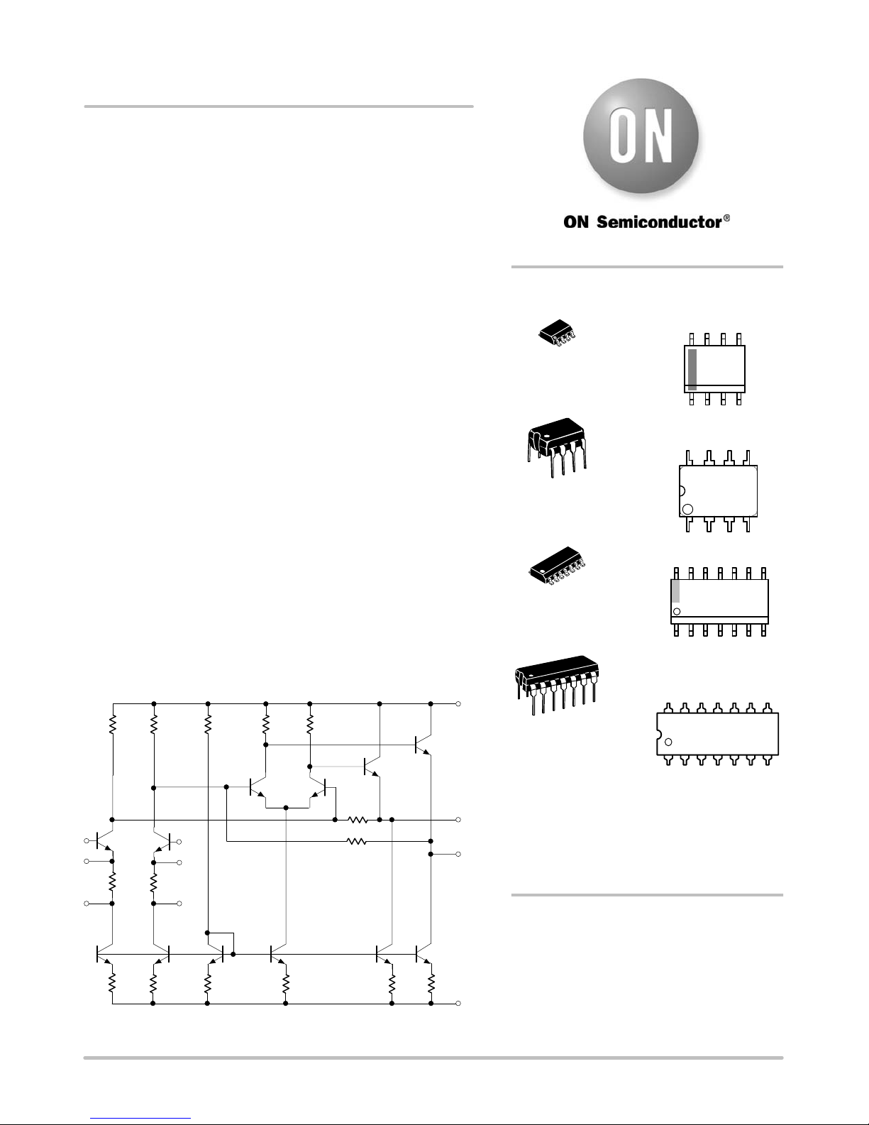
+V
Q6
OUTPUT 1
OUTPUT 2
R1 R2 R8 R10 R9
Q5
Q4 Q3
R11
R12
Q11
Q10
R13 R14R16R15R7BR7A
Q7B Q8 Q9
Q7A
G2A
G1A
INPUT 1 INPUT 2
R3 R5
G1B
G2B
Q1 Q2
-V
Figure 1. Block Diagram
NE592
http://onsemi.com
2
PIN CONNECTIONS
1
2
3
45
6
7
8
1
2
3
4
5
6
78
14
13
12
11
10
9
INPUT 1
NC
G2A GAIN SELECT
G1A GAIN SELECT
V+
NC
OUTPUT 1
INPUT 2
NC
G2B GAIN SELECT
G1B GAIN SELECT
V-
NC
OUTPUT 2
INPUT 2
V-
OUTPUT 2
INPUT 1
V+
OUTPUT 1
G1A GAIN SELECT
G1B GAIN SELECT
D, N Packages D, N Packages
(Top View)
(Top View)
MAXIMUM RATINGS (TA= +25°C, unless otherwise noted.)
Rating Symbol Value Unit
Supply Voltage VCC "8.0 V
Differential Input Voltage VIN "5.0 V
Common-Mode Input Voltage VCM "6.0 V
Output Current IOUT 10 mA
Operating Ambient Temperature Range TA0 to +70 °C
Operating Junction Temperature TJ150 °C
Storage Temperature Range TSTG 65 to +150 °C
Maximum Power Dissipation, TA= 25°C (Still Air) (Note 1)
D-14 Package
D-8 Package
N-14 Package
N-8 Package
PDMAX
0.98
0.79
1.44J1.17
W
Thermal Resistance, Junction−to−Ambient
D-14 Package
D-8 Package
N-14 Package
N-8 Package
RqJA 145
182
100
130
°C/W
Stresses exceeding Maximum Ratings may damage the device. Maximum Ratings are stress ratings only. Functional operation above the
Recommended Operating Conditions is not implied. Extended exposure to stresses above the Recommended Operating Conditions may affect
device reliability.
1. Derate above 25°C at the following rates:
D-14 package at 6.9 mW/°C
D-8 package at 5.5 mW/°C
N-14 package at 10 mW/°C
N-8 package at 7.7 mW/°C.

NE592
http://onsemi.com
3
DC ELECTRICAL CHARACTERISTICS (VSS = "6.0 V, VCM = 0, typicals at TA= +25°C, min and max at 0°C vTAv70°C, unless
otherwise noted. Recommended operating supply voltages VS= "6.0 V.)
Characteristic Test Conditions Symbol Min Typ Max Unit
Differential Voltage Gain
Gain 1 (Note 2)
Gain 2 (Notes 3 and 4)
RL= 2.0 kW, VOUT = 3.0 VP-P
AVOL 250
80
400
100
600
120
V/V
Input Resistance
Gain 1 (Note 2)
Gain 2 (Notes 3 and 4)
−
TA= 25°C
0°C vTAv70°C
RIN
−
10
8.0
4.0
30
−
−
−
−
kW
Input Capacitance Gain 2 (Note 4) CIN −2.0 −pF
Input Offset Current TA= 25°C
0°C vTAv70°C
IOS −
−
0.4
−
5.0
6.0
mA
Input Bias Current TA= 25°C
0°C vTAv70°C
IBIAS −
−
9.0
−
30
40
mA
Input Noise Voltage BW 1.0 kHz to 10 MHz VNOISE −12 −mVRMS
Input Voltage Range −VIN "1.0 − − V
Common-Mode Rejection Ratio
Gain 2 (Note 4)
VCM "1.0 V, f < 100 kHz, TA= 25°C
VCM "1.0 V, f < 100 kHz,
0°C vTAv70°C
VCM "1.0 V, f < 5.0 MHz
CMRR 60
50
−
86
−
60
−
−
−
dB
Supply Voltage Rejection Ratio
Gain 2 (Note 4)
DVS= "0.5 V PSRR 50 70 −dB
Output Offset Voltage
Gain 1
Gain 2 (Note 4)
Gain 3 (Note 5)
Gain 3 (Note 5)
RL= R
RL= R
RL= R, TA= 25°C
RL= R, 0°C vTAv70°C
VOS
−
−
−
−
−
−
0.35
−
1.5
1.5
0.75
1.0
V
Output Common-Mode Voltage RL= R, TA= 25°C VCM 2.4 2.9 3.4 V
Output Voltage Swing Differential RL= 2.0 kW, TA= 25°C
RL= 2.0 kW, 0°C vTAv70°C
VOUT 3.0
2.8
4.0
−
−
−
V
Output Resistance −ROUT −20 −W
Power Supply Current RL= R, TA= 25°C
RL= R, 0°C vTAv70°C
ICC −
−
18
−
24
27
mA
AC ELECTRICAL CHARACTERISTICS (TA= +25°CVSS = "6.0 V, VCM = 0, unless otherwise noted. Recommended operating
supply voltages VS= "6.0 V.)
Characteristic Test Conditions Symbol Min Typ Max Unit
Bandwidth
Gain 1 (Note 2)
Gain 2 (Notes 3 and 4)
−BW
−
−
40
90
−
−
MHz
Rise Time
Gain 1 (Note 2)
Gain 2 (Notes 3 and 4)
VOUT = 1.0 VP−P
tR
−
−
10.5
4.5
12
−
ns
Propagation Delay
Gain 1 (Note 2)
Gain 2 (Notes 3 and 4)
VOUT = 1.0 VP−P
tPD
−
−
7.5
6.0
10
−
ns
2. Gain select Pins G1A and G1B connected together.
3. Gain select Pins G2A and G2B connected together.
4. Applies to 14-pin version only.
5. All gain select pins open.
NE592
http://onsemi.com
4
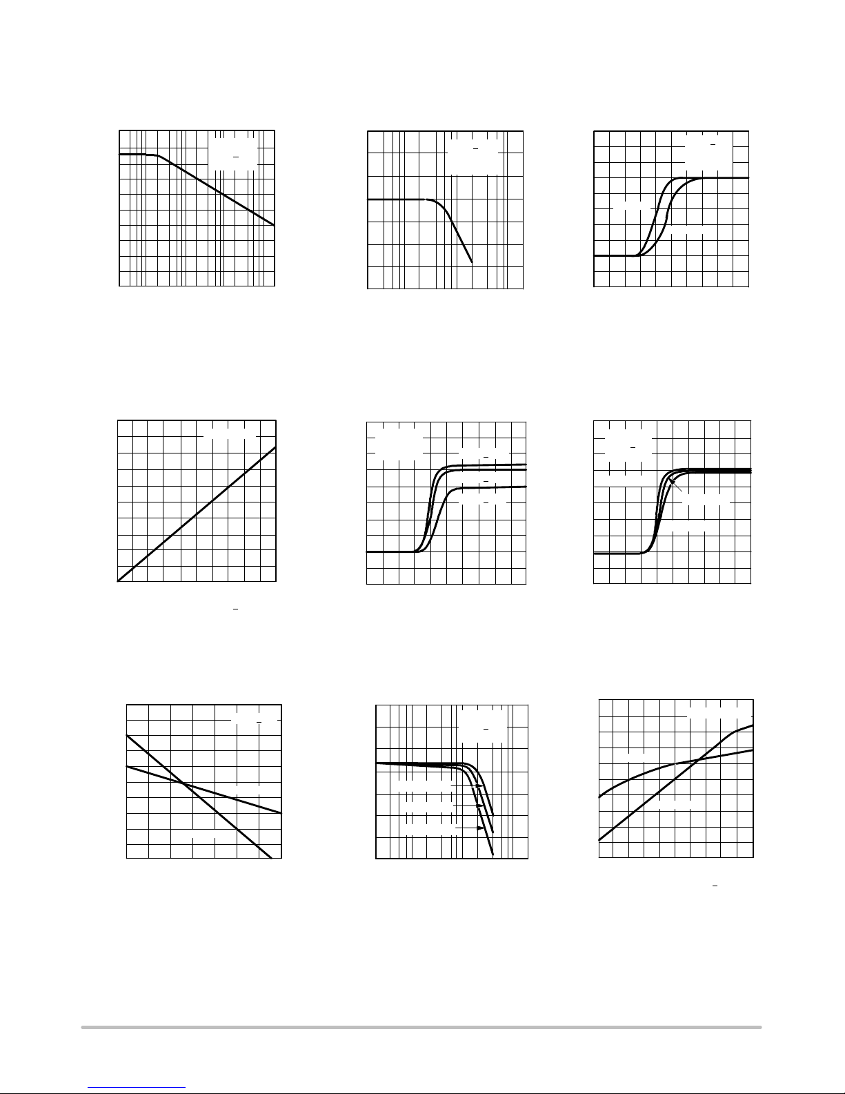
TYPICAL PERFORMANCE CHARACTERISTICS
COMMON-MODE REJECTION RATIO −dB
100
90
80
70
60
50
40
30
20
10
0
10k 100k 1M 10M 100M
FREQUENCY −Hz
GAIN 2
VS= +6V
TA= 25oC
OUTPUT VOLTAGE SWING −Vpp
7.0
6.0
5.0
4.0
3.0
2.0
1.0
0
1 5 10 50 100 500 1000
FREQUENCY −MHz
VS= +6V
TA= 25oC
RL= 1kW
1.6
1.4
1.2
1.0
0.8
0.6
0.4
0.2
0
-0.2
-0.4
-15 -10 -5 0 5 10 15 20 25 30 35
TIME −ns
VS= +6V
TA= 25oC
RL= 1k
GAIN 2
GAIN 1
Figure 2. Common−Mode
Rejection Ratio as a Function
of Frequency
Figure 3. Output Voltage Swing
as a Function of Frequency
Figure 4. Pulse Response
SUPPLY CURRENT −mA
28
24
20
16
12
8
34 5678
SUPPLY VOLTAGE −+V
TA= 25oC
OUTPUT VOLTAGE −V
1.6
1.4
1.2
1.0
0.8
0.6
0.4
0.2
0
-0.2
-0.4
-15 -10 -5 0 5 10 15 20 25 30 35
TIME −ns
GAIN 2
TA= 25oC
RL= 1kWVS= +8V
VS= +3V
VS= +6V
TA= 70oC
Tamb = 0oC
OUTPUT VOLTAGE −V
1.6
1.4
1.2
1.0
0.8
0.6
0.4
0.2
0
-0.2
-0.4
-15 -10 -5 0 5 10 15 20 25 30 35
TIME −ns
GAIN 2
VS= +6V
RL= 1kW
TA= 25oC
Figure 5. Supply Current as
a Function of Temperature
Figure 6. Pulse Response as
a Function of Supply Voltage
Figure 7. Pulse Response as
a Function of Temperature
RELATIVE VOLTAGE GAIN
1.10
1.08
1.06
1.04
1.02
1.00
0.98
0.96
0.94
0.92
0.90
0 102030 405060 70
TEMPERATURE −oC
VS= +6V
GAIN 2
GAIN 1
SINGLE ENDED VOLTAGE GAIN −dB
60
50
40
30
20
10
0
-10
1 5 10 50 100 500 1000
FREQUENCY −MHz
GAIN 2
VS= +6V
RL= 1kW
TA= 125oC
TA= −55oC
TA= 25oC
RELATIVE VOLTAGE GAIN
1.4
1.3
1.2
1.1
1.0
0.9
0.8
0.7
0.6
0.5
0.4
34567 8
SUPPLY VOLTAGE −+V
Tamb = 25oC
GAIN 2
GAIN 1
Figure 8. Voltage Gain as a
Function of Temperature
Figure 9. Gain vs. Frequency
as a Function of Temperature
Figure 10. Voltage Gain as a
Function of Supply Voltage

NE592
http://onsemi.com
5
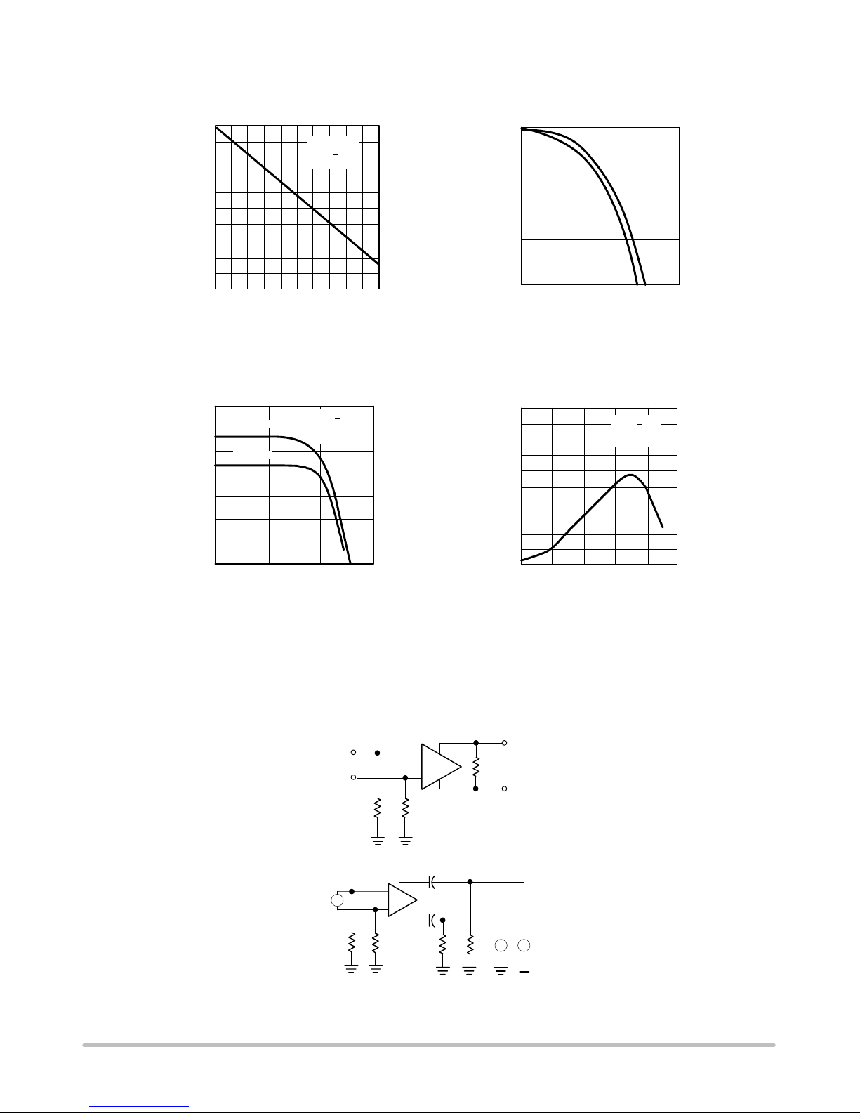
TYPICAL PERFORMANCE CHARACTERISTICS
SINGLE ENDED VOLTAGE GAIN −dB
60
50
40
30
20
10
0
-10
1 5 10 50 100 500 1000
FREQUENCY −MHz
VS= +8V
VS= +3V
VS= +6V
GAIN 2
TA= 25oC
RL= 1kW14
1
1211 8
7
4
3
0.2mF
0.2mF
592
51WRADJ 1kW1kW
TA= 25oCVS= +6V
DIFFERENTIAL VOLTAGE GAIN −V/V
1000
100
10
1
.1
.01
1 10 100 1K 10K 100K 1M
RADJ −W
VS= +6V
f = 100kHz
TA= 25oC
FIGURE 2
Figure 11. Gain vs. Frequency
as a Function of Supply Voltage
Figure 12. Voltage Gain Adjust
Circuit
Figure 13. Voltage Gain as a
Function of RADJ (Figure 2)
SUPPLY CURRENT −mA
21
20
19
18
17
16
15
14
-60 -20 20 60 100 140
TEMPERATURE −oC
VS= +6V
OVERDRIVE RECOVERY TIME −ns
70
60
50
40
30
20
10
0
0 20 40 60 80 100 120 140 160 180 200
DIFFERENTIAL INPUT VOLTAGE −mV
VS= +6V
TA= 25oC
GAIN 2
OUTPUT VOLTAGE SWING −V OR
OUTPUT SINK CURRENT −mA
7.0
6.0
5.0
4.0
3.0
2.0
1.0
0
3.0 4.0 5.0 6.0 7.0 8.0
SUPPLY VOLTAGE −+V
TA= 25oC
VOLTAGE
CURRENT
OUTPUT VOLTAGE SWING −Vpp
7.0
6.0
5.0
4.0
3.0
2.0
1.0
0
10 50 100 500 1K 5K 10K
LOAD RESISTANCE −W
VS= +6V
TA= 25oC
Figure 14. Supply Current as a
Function of Temperature
Figure 15. Differential Overdrive
Recovery Time
Figure 16. Output Voltage and
Current Swing as a Function of
Supply Voltage
INPUT RESISTANCE −K
70
60
50
40
30
20
10
0
-60 -20 0 20 60 100 140
TEMPERATURE −oC
GAIN 2
VS= +6V
Ω
INPUT NOISE VOLTAGE −Vrms
100
90
80
70
60
50
40
30
20
10
0
1 10 100 1K 10K
SOURCE RESISTANCE −W
GAIN 2
VS= +6V
TA= 25oC
BW = 10MHz
μ
Figure 17. Output Voltage
Swing as a Function of Load
Resistance
Figure 18. Input Resistance as a
Function of Temperature
Figure 19. Input Noise Voltage
as a Function of Source
Resistance
51W
NE592
http://onsemi.com
6
TYPICAL PERFORMANCE CHARACTERISTICS
PHASE SHIFT −DEGREES
0
-5
-10
-15
-20
-25
012345678910
FREQUENCY −MHz
GAIN 2
VS= +6V
TA= 25oC
VOLTAGE GAIN −dB
60
50
40
30
20
10
0
1 10 100 1000
FREQUENCY −MHz
VS= +6V
Tamb = 25oC
RL= 1KW
GAIN 1
GAIN 2
Figure 20. Phase Shift as a
Function of Frequency
Figure 21. Phase Shift as a
Function of Frequency
Figure 22. Voltage Gain as a
Function of Frequency
PHASE SHIFT −DEGREES
0
-50
-100
-150
-200
-250
-300
-350
1 10 100 1000
FREQUENCY −MHz
VS= +6V
TA= 25oC
GAIN 1
GAIN 2
VOLTAGE GAIN −dB
.01 .1 1 10 100 1000
40
30
20
10
0
-10
-20
-30
-40
-50
FREQUENCY −MHz
VS= +6V
TA= 25oC
GAIN 3
Figure 23. Voltage Gain as a
Function of Frequency
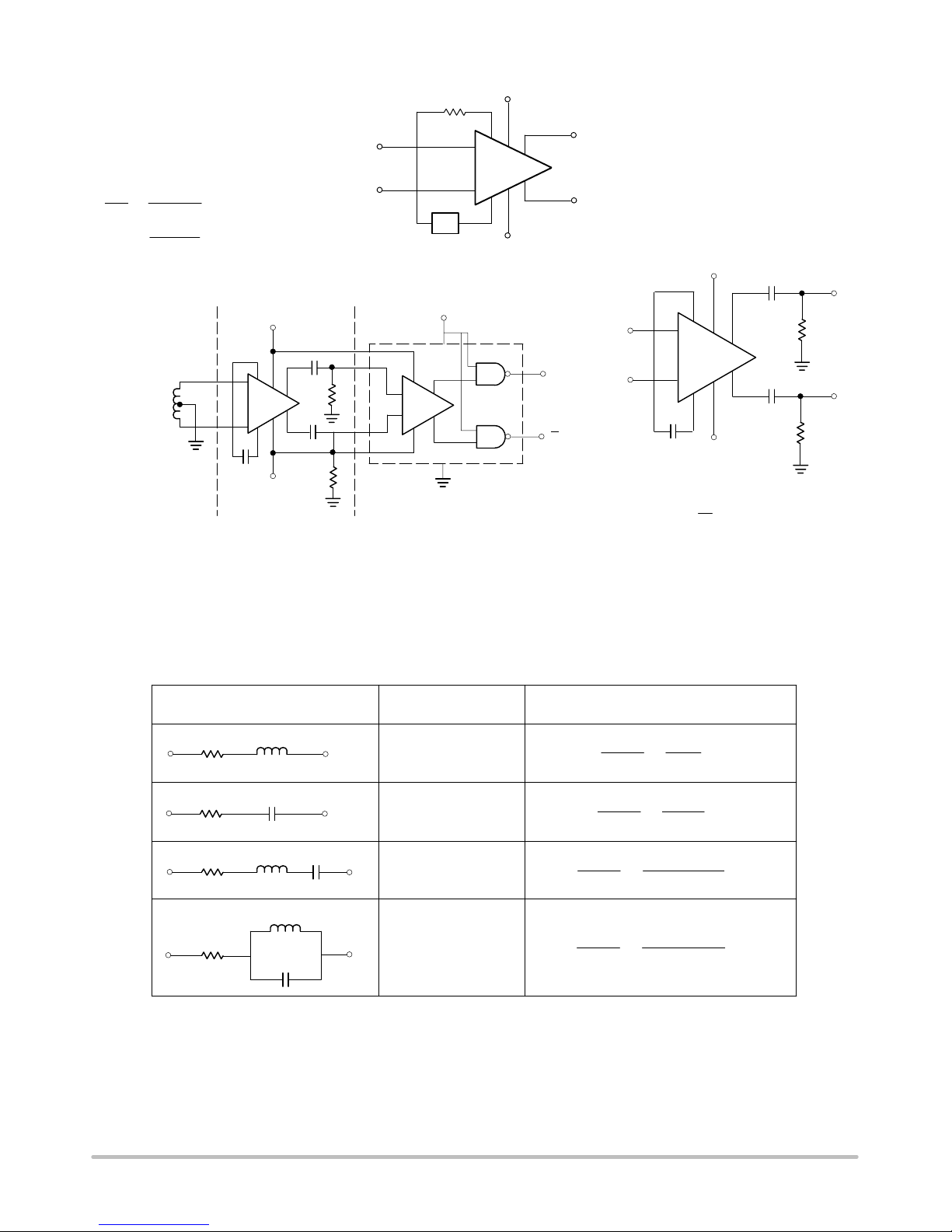
VIN VOUT
RL
592
51W51W
51W51W
ein
eout eout
1kW1kW
0.2mF
0.2mF
592
TEST CIRCUITS (TA= 25°C, unless otherwise noted.)
Figure 24. Test Circuits
NE592
http://onsemi.com
7
NOTE:
Basic Configuration
Disc/Tape Phase-Modulated Readback Systems
Differentiation with High
Common-Mode Noise Rejection
NOTE:
For frequency F1<< 1/2 π(32) C
VO]1.4 x 10⁴CdVi
dT
Z
V1
2re
+6
V0
7
5
4
1
14 11
10
-6
592
READ HEAD DIFFERENTIATOR/AMPLIFIER ZERO CROSSING DETECTOR
+5
948
529 7
5
Q
Q
6
3
2
1
10
+6
14 11
10 8
7
5
4
1
-6
AMPLITUDE: 1-10 mV p-p
FREQUENCY: 1-4 MHz
592
0.2mF
+6
0.2mF
2KW
2KW
V0
V1
C
14
1
11
4
10
5
7
8
-6
592
V0(s)
v1(s) [1.4 @104
Z(S) )2re
[1.4 @104
Z(S) )32
Figure 25. Typical Applications
NOTES:
In the networks above, the R value used is assumed to include 2re, or approximately 32W.
S = jW
W= 2πf
1.4 104
Lƪ1
s)RńLƫ
1.4 104
Rƪs
s)1ńRCƫ
1.4 104
Lƪs
s2)RńLs )1ńLCƫ
1.4 104
Rƪs2)1ńLC
s2)1ńLC )sńRCƫ
Z NETWORK FILTER
TYPE
V0(s) TRANSFER
V1(s) FUNCTION
LOW PASS
HIGH PASS
BAND PASS
BAND REJECT
RL
RC
RLC
R
L
C
Figure 26. Filter Networks
NE592
http://onsemi.com
8
ORDERING INFORMATION
Device Temperature Range Package Shipping†
NE592D8
0 to +70°C
SOIC−8
98 Units/Rail
NE592D8G SOIC−8
(Pb−Free)
NE592D8R2 SOIC−8
2500 / Tape & Reel
NE592D8R2G SOIC−8
(Pb−Free)
NE592N8 PDIP−8
50 Units/Rail
NE592N8G PDIP−8
(Pb−Free)
NE592D14 SOIC−14
55 Units/Rail
NE592D14G SOIC−14
(Pb−Free)
NE592D14R2 SOIC−14
2500 / Tape & Reel
NE592D14R2G SOIC−14
(Pb−Free)
NE592N14 PDIP−14
25 Units/Rail
NE592N14G PDIP−14
(Pb−Free)
†For information on tape and reel specifications, including part orientation and tape sizes, please refer to our Tape and Reel Packaging Specification
Brochure, BRD8011/D.

NE592
http://onsemi.com
9
PACKAGE DIMENSIONS
SOIC−8 NB
CASE 751−07
ISSUE AH
SEATING
PLANE
1
4
58
N
J
X 45_
K
NOTES:
1. DIMENSIONING AND TOLERANCING PER
ANSI Y14.5M, 1982.
2. CONTROLLING DIMENSION: MILLIMETER.
3. DIMENSION A AND B DO NOT INCLUDE
MOLD PROTRUSION.
4. MAXIMUM MOLD PROTRUSION 0.15 (0.006)
PER SIDE.
5. DIMENSION D DOES NOT INCLUDE DAMBAR
PROTRUSION. ALLOWABLE DAMBAR
PROTRUSION SHALL BE 0.127 (0.005) TOTAL
IN EXCESS OF THE D DIMENSION AT
MAXIMUM MATERIAL CONDITION.
6. 751−01 THRU 751−06 ARE OBSOLETE. NEW
STANDARD IS 751−07.
A
BS
D
H
C
0.10 (0.004)
DIM
A
MIN MAX MIN MAX
INCHES
4.80 5.00 0.189 0.197
MILLIMETERS
B3.80 4.00 0.150 0.157
C1.35 1.75 0.053 0.069
D0.33 0.51 0.013 0.020
G1.27 BSC 0.050 BSC
H0.10 0.25 0.004 0.010
J0.19 0.25 0.007 0.010
K0.40 1.27 0.016 0.050
M0 8 0 8
N0.25 0.50 0.010 0.020
S5.80 6.20 0.228 0.244
−X−
−Y−
G
M
Y
M
0.25 (0.010)
−Z−
Y
M
0.25 (0.010) ZSXS
M
____
1.52
0.060
7.0
0.275
0.6
0.024
1.270
0.050
4.0
0.155
ǒmm
inchesǓ
SCALE 6:1
*For additional information on our Pb−Free strategy and soldering
details, please download the ON Semiconductor Soldering and
Mounting Techniques Reference Manual, SOLDERRM/D.
SOLDERING FOOTPRINT*
NE592
http://onsemi.com
10
PACKAGE DIMENSIONS
PDIP−8
N SUFFIX
CASE 626−05
ISSUE L
NOTES:
1. DIMENSION L TO CENTER OF LEAD WHEN
FORMED PARALLEL.
2. PACKAGE CONTOUR OPTIONAL (ROUND OR
SQUARE CORNERS).
3. DIMENSIONING AND TOLERANCING PER ANSI
Y14.5M, 1982.
14
58
F
NOTE 2 −A−
−B−
−T−
SEATING
PLANE
H
J
G
DK
N
C
L
M
M
A
M
0.13 (0.005) B M
T
DIM MIN MAX MIN MAX
INCHESMILLIMETERS
A9.40 10.16 0.370 0.400
B6.10 6.60 0.240 0.260
C3.94 4.45 0.155 0.175
D0.38 0.51 0.015 0.020
F1.02 1.78 0.040 0.070
G2.54 BSC 0.100 BSC
H0.76 1.27 0.030 0.050
J0.20 0.30 0.008 0.012
K2.92 3.43 0.115 0.135
L7.62 BSC 0.300 BSC
M−−− 10 −−− 10
N0.76 1.01 0.030 0.040
__

NE592
http://onsemi.com
11
PACKAGE DIMENSIONS
SOIC−14
CASE 751A−03
ISSUE H
NOTES:
1. DIMENSIONING AND TOLERANCING PER
ANSI Y14.5M, 1982.
2. CONTROLLING DIMENSION: MILLIMETER.
3. DIMENSIONS A AND B DO NOT INCLUDE
MOLD PROTRUSION.
4. MAXIMUM MOLD PROTRUSION 0.15 (0.006)
PER SIDE.
5. DIMENSION D DOES NOT INCLUDE
DAMBAR PROTRUSION. ALLOWABLE
DAMBAR PROTRUSION SHALL BE 0.127
(0.005) TOTAL IN EXCESS OF THE D
DIMENSION AT MAXIMUM MATERIAL
CONDITION.
−A−
−B−
G
P7 PL
14 8
7
1
M
0.25 (0.010) B M
S
B
M
0.25 (0.010) A S
T
−T−
F
RX 45
SEATING
PLANE D14 PL K
C
J
M
_DIM MIN MAX MIN MAX
INCHESMILLIMETERS
A8.55 8.75 0.337 0.344
B3.80 4.00 0.150 0.157
C1.35 1.75 0.054 0.068
D0.35 0.49 0.014 0.019
F0.40 1.25 0.016 0.049
G1.27 BSC 0.050 BSC
J0.19 0.25 0.008 0.009
K0.10 0.25 0.004 0.009
M0 7 0 7
P5.80 6.20 0.228 0.244
R0.25 0.50 0.010 0.019
__ __
7.04
14X
0.58
14X
1.52
1.27
DIMENSIONS: MILLIMETERS
1
PITCH
SOLDERING FOOTPRINT*
7X
*For additional information on our Pb−Free strategy and soldering
details, please download the ON Semiconductor Soldering and
Mounting Techniques Reference Manual, SOLDERRM/D.
NE592
http://onsemi.com
12
PACKAGE DIMENSIONS
PDIP−14
CASE 646−06
ISSUE P
17
14 8
B
ADIM MIN MAX MIN MAX
MILLIMETERSINCHES
A0.715 0.770 18.16 19.56
B0.240 0.260 6.10 6.60
C0.145 0.185 3.69 4.69
D0.015 0.021 0.38 0.53
F0.040 0.070 1.02 1.78
G0.100 BSC 2.54 BSC
H0.052 0.095 1.32 2.41
J0.008 0.015 0.20 0.38
K0.115 0.135 2.92 3.43
L
M−−− 10 −−− 10
N0.015 0.039 0.38 1.01
__
NOTES:
1. DIMENSIONING AND TOLERANCING PER ANSI
Y14.5M, 1982.
2. CONTROLLING DIMENSION: INCH.
3. DIMENSION L TO CENTER OF LEADS WHEN
FORMED PARALLEL.
4. DIMENSION B DOES NOT INCLUDE MOLD FLASH.
5. ROUNDED CORNERS OPTIONAL.
F
HG D
K
C
SEATING
PLANE
N
−T−
14 PL
M
0.13 (0.005)
L
M
J0.290 0.310 7.37 7.87
ON Semiconductor and are registered trademarks of Semiconductor Components Industries, LLC (SCILLC). SCILLC reserves the right to make changes without further notice
to any products herein. SCILLC makes no warranty, representation or guarantee regarding the suitability of its products for any particular purpose, nor does SCILLC assume any
liability arising out of the application or use of any product or circuit, and specifically disclaims any and all liability, including without limitation special, consequential or incidental
damages. “Typical” parameters which may be provided in SCILLC data sheets and/or specifications can and do vary in different applications and actual performance may vary over
time. All operating parameters, including “Typicals” must be validated for each customer application by customer’s technical experts. SCILLC does not convey any license under
its patent rights nor the rights of others. SCILLC products are not designed, intended, or authorized for use as components in systems intended for surgical implant into the body,
or other applications intended to support or sustain life, or for any other application in which the failure of the SCILLC product could create a situation where personal injury or death
may occur. Should Buyer purchase or use SCILLC products for any such unintended or unauthorized application, Buyer shall indemnify and hold SCILLC and its officers, employees,
subsidiaries, affiliates, and distributors harmless against all claims, costs, damages, and expenses, and reasonable attorney fees arising out of, directly or indirectly, any claim of
personal injury or death associated with such unintended or unauthorized use, even if such claim alleges that SCILLC was negligent regarding the design or manufacture of the part.
SCILLC is an Equal Opportunity/Affirmative Action Employer. This literature is subject to all applicable copyright laws and is not for resale in any manner.
PUBLICATION ORDERING INFORMATION
N. American Technical Support: 800−282−9855 Toll Free
USA/Canada
Europe, Middle East and Africa Technical Support:
Phone: 421 33 790 2910
Japan Customer Focus Center
Phone: 81−3−5773−3850
NE592/D
LITERATURE FULFILLMENT:
Literature Distribution Center for ON Semiconductor
P.O. Box 5163, Denver, Colorado 80217 USA
Phone: 303−675−2175 or 800−344−3860 Toll Free USA/Canada
Fax: 303−675−2176 or 800−344−3867 Toll Free USA/Canada
Email: [email protected]
ON Semiconductor Website: www.onsemi.com
Order Literature: http://www.onsemi.com/orderlit
For additional information, please contact your local
Sales Representative
Table of contents


