SG Micro SGM5200 User manual

SGM5200
12-Bit, 1MSPS, 16 Channels,
Single-Ended, Serial Interface ADC
SG Micro Corp
www.sg-micro.com
SEPTEMBER 2021 –REV. A
GENERAL DESCRIPTION
The SGM5200 is a 12-bit multichannel inputs
analog-to-digital converter (ADC). The device includes
a capacitor based SAR ADC with inherent sample and
hold circuit.
The SGM5200 accepts a wide power supply range
from 2.7V to 5.25V. Very low power consumption
makes the device suitable for battery-powered or
isolated power supply applications.
A wide 1.7V to 5.25V digital I/O power supply range
facilitates a glueless interface with the most commonly
used digital hosts. The serial interface is controlled by
nCS and SCLK for easy connection with
microprocessors and DSP.
The input signal is sampled with the falling edge of nCS.
It uses SCLK for conversion, serial data output and
reading serial data in. The device allows auto
sequencing of preselected channels or manual selection
of a channel for the next conversion cycle.
There are two software selectable input ranges (0V to
VREF and 0V to 2 × VREF), individually configurable GPIOs
(four in case of the TSSOP package and one in TQFN
package) and two programmable alarm thresholds per
channel. These features make the device suitable for
most data acquisition applications.
The SGM5200 offers an attractive power-down feature.
This is extremely useful for power saving when the
device is operated at lower conversion speeds.
The SGM5200 is available in Green TSSOP-38 and
TQFN-5×5-32L packages. It operates over an ambient
temperature range -40℃to +125℃.
FEATURES
●1MHz Sample Rate
●12-Bit Resolution
●16 Channels
●Zero Latency
●20MHz Serial Interface
●Analog Power Supply Range: 2.7V to 5.25V
●Digital I/O Power Supply Range: 1.7V to 5.25V
●Two Software Selectable Unipolar, Input Ranges
Range 1: 0V to VREF
Range 2: 0V to 2 × VREF
●Auto and Manual Modes for Channel Selection
●Two Programmable Alarm Thresholds per
Channel
●Four Individually Configurable GPIOs in TSSOP
Package and One GPIO in TQFN Package
●Typical Power Dissipation:
24mW (VA= 5V, VBD = 3V) at 1MSPS
●Power-Down Current: 1.4μA (TYP)
●Input Bandwidth: 45MHz (TYP) at -3dB
●Available in Green TSSOP-38 and TQFN-5×5-32L
Packages
APPLICATIONS
PLC/IPC
Optical Line Card Monitoring
Medical Instrumentation
Digital Power Supplies
Multichannel, General-Purpose Signal Monitoring
High-Speed Data Acquisition Systems
High-Speed Closed-Loop Systems

12-Bit, 1MSPS, 16 Channels,
SGM5200 Single-Ended, Serial Interface ADC
2
SEPTEMBER 2021
SG Micro Corp
www.sg-micro.com
PACKAGE/ORDERING INFORMATION
MODEL PACKAGE
DESCRIPTION
SPECIFIED
TEMPERATURE
RANGE
ORDERING
NUMBER
PACKAGE
MARKING
PACKING
OPTION
SGM5200
TSSOP-38 -40℃to +125℃SGM5200XTS38G/TR
SGM5200
XTS38
XXXXX
Tape and Reel, 4000
TQFN-5×5-32L -40℃to +125℃SGM5200XTQL32G/TR
SGM5200
XTQL32
XXXXX
Tape and Reel, 3000
MARKING INFORMATION
NOTE: XXXXX = Date Code, Trace Code and Vendor Code.
Trace Code
Vendor Code
Date Code - Year
X XXX X
Green (RoHS & HSF): SG Micro Corp defines "Green" to mean Pb-Free (RoHS compatible) and free of halogen substances. If
you have additional comments or questions, please contact your SGMICRO representative directly.
ABSOLUTE MAXIMUM RATINGS
AINP or CHx to AGND .............................. -0.3V to VA+ 0.3V
+VA to AGND, +VBD to BDGND ......................... -0.3V to 6V
Digital Input Voltage to BDGND........................... -0.3V to 6V
Digital Output to BDGND .......................... -0.3V to VA+ 0.3V
Input Current to Any Pin except Supply Pins..... -10mA to 10mA
Junction Temperature.................................................+150℃
Storage Temperature Range ....................... -65℃to +150℃
Lead Temperature (Soldering, 10s) ............................+260℃
ESD Susceptibility
HBM............................................................................. 4000V
CDM ............................................................................ 1000V
RECOMMENDED OPERATING CONDITIONS
Analog Power Supply Voltage Range...............2.7V to 5.25V
Digital I/O Power Supply Voltage Range ............... 1.7V to VA
Reference Voltage Range.........................................2V to 3V
SCLK Frequency ........................................................ 20MHz
Operating Temperature Range .................... -40℃to +125℃
OVERSTRESS CAUTION
Stresses beyond those listed in Absolute Maximum Ratings
may cause permanent damage to the device. Exposure
to
absolute maximum rating conditions for extended periods
may affect reliability. Functional operation of the device at any
conditions beyond those indicated in the Recommended
Operating Conditions section
is not implied.
ESD SENSITIVITY CAUTION
This integrated circuit can be damaged if ESD protections are
not considered carefully. SGMICRO recommends that all
integrated circuits be handled with appropriate precautions.
Failure
to observe proper handling
and installation procedures
can cause damage. ESD damage can range from subtle
performance
degradation to
complete device failure. Precision
integrated circuits may be more susceptible to damage
because even small parametric changes could cause the
device not to meet the published specifications.
DISCLAIMER
SG Micro Corp reserves the right to make any change in
circuit
design, or specifications
without prior notice.

12-Bit, 1MSPS, 16 Channels,
SGM5200 Single-Ended, Serial Interface ADC
3
SEPTEMBER 2021
SG Micro Corp
www.sg-micro.com
PIN CONFIGURATIONS
(TOP VIEW)
1
2
3
4
5
7
8
9
10
6
11
12
13
14
15
17
18
19
16
38
37
36
35
34
32
31
30
29
33
28
27
26
25
24
22
21
20
23
GPIO2
GPIO3
REFM
REFP
+VA
AGND
MXO
AINP
AINM
AGND
CH15
CH14
CH13
CH12
CH11
CH10
CH9
CH8
AGND
GPIO1
GPIO0
+VBD
BDGND
SDO
SDI
SCLK
nCS
AGND
+VA
CH0
CH1
CH2
CH3
CH4
CH5
CH6
CH7
AGND
TSSOP-38
(TOP VIEW)
MXO
AINP
CH15
AGND
AINM
SCLK
nCS
CH0
+VA
CH3
1
4
3
2
7
8
5
6
24
21
22
23
18
17
20
19
9 10 11 12 13 14 15 16
32 31 30 29 28 27 26 25
AGND
CH13
CH12
CH14
AGND
CH2
CH1
CH11
CH10
CH9
CH8
CH7
CH6
CH5
CH4
+VA
REFP
REFM
GPIO0
+VBD
BDGND
SDO
SDI
TQFN-5×5-32L
12-Bit, 1MSPS, 16 Channels,
SGM5200 Single-Ended, Serial Interface ADC
4
SEPTEMBER 2021
SG Micro Corp
www.sg-micro.com
PIN DESCRIPTION
PIN NAME TYPE (1) FUNCTION
TSSOP-38 TQFN-5×5-32L
1 ‒
GPIO2 DIO General-Purpose Input or Output.
Range DI
Selects ADC Input Range
High (1): select Range 2 (0V to 2 × VREF),
Low (0): select Range 1 (0V to VREF).
2 ‒GPIO3 DIO General-Purpose Input or Output.
nPD DI Active Low Power-Down Input.
3 30 REFM AI Reference Ground.
4 31 REFP AI Reference Input.
5, 29 21, 32 +VA ‒Analog Power Supply.
6, 10, 19, 20, 30 1, 22 AGND ‒Analog Ground.
7 2 MXO AO Multiplexer Output.
8 3 AINP AI ADC Input Signal.
9 4 AINM AI ADC Input Ground.
11 5 CH15 AI
Analog Channel for Multiplexer.
12 6 CH14 AI
13 7 CH13 AI
14 8 CH12 AI
15 9 CH11 AI
16 10 CH10 AI
17 11 CH9 AI
18 12 CH8 AI
21 13 CH7 AI
22 14 CH6 AI
23 15 CH5 AI
24 16 CH4 AI
25 17 CH3 AI
26 18 CH2 AI
27 19 CH1 AI
28 20 CH0 AI
31 23 nCS DI Chip-Select Input Pin. Active low.
32 24 SCLK DI Serial Clock Input Pin.
33 25 SDI DI Serial Data Input Pin.
34 26 SDO DI Serial Data Output Pin.
35 27 BDGND ‒Digital Ground.
36 28 +VBD ‒Digital Power Supply.
37 29 GPIO0 DIO General-Purpose Input or Output.
Alarm DO Active High Alarm Output. For configuration, see the Programming section.
38 ‒GPIO1 DIO General-Purpose Input or Output.
Low Alarm DO Active High Output Indicating Low Alarm.
NOTE:
1. AI = Analog Input, AO = Analog Output, DI = Digital Input, DO = Digital Output, DIO = Digital Input or Output.
12-Bit, 1MSPS, 16 Channels,
SGM5200 Single-Ended, Serial Interface ADC
5
SEPTEMBER 2021
SG Micro Corp
www.sg-micro.com
ELECTRICAL CHARACTERISTICS
(VA= 2.7V to 5.25V, VBD = 1.7V to VA, VREF = 2.5V ±0.1V, fSAMPLE = 1MHz, Full = -40℃to +125℃, typical values are at TA=
+25℃, unless otherwise noted.)
PARAMETER SYMBOL
CONDITIONS MIN TYP MAX UNITS
Analog Input
Full-Scale Input Span (1) Range 1 0 VREF V
Range 2 while 2 × VREF ≤ VA0 2 × VREF
Absolute Input Range Range 1 -0.2 VREF + 0.2 V
Range 2 while 2 × VREF ≤ VA-0.2 2 × VREF + 0.2
Input Capacitance 31 pF
Input Leakage Current TA= +125℃60 nA
System Performance
Resolution 12 Bits
No Missing Codes Range 1 11 Bits
Range 2 12
Integral Linearity Range 1 -3.50 ±1.6 2.60 LSB (2)
Range 2 -1.32 ±0.8 1.32
Differential Linearity Range 1 -1.00 -1/+1.3 2.20 LSB
Range 2 -0.99 ±0.5 1.00
Offset Error (3) Range 1 -4.00 ±0.6 4.00 LSB
Range 2 -5.60 ±1.6 5.60
Gain Error Range 1 -5.20 ±0.8 4.40 LSB
Range 2 -4.10 ±0.8 3.10
Total Unadjusted Error TUE Range 1 ±1.8 LSB
Range 2 ±1.9
Sampling Dynamics
Conversion Time 20MHz SCLK 800 ns
Acquisition Time 325 ns
Maximum Throughput Rate 20MHz SCLK 1 MHz
Aperture Delay 6 ns
Dynamic Characteristics
Total Harmonic Distortion (4) THD 100kHz Range 1 -77 dB
Range 2 -79
Signal-to-Noise Ratio SNR 100kHz Range 1 66.4 70.4 dB
Range 2 67.9 71.4
Signal-to-Noise + Distortion 100kHz Range 1 65.6 69.5 dB
Range 2 66.7 70.7
Spurious Free Dynamic Range
100kHz Range 1 78 dB
Range 2 81
Small Signal Bandwidth At -3dB 45 MHz
Channel-to-Channel Crosstalk
Any off-channel with 100kHz, full-scale
input to channel being sampled with DC
input (isolation crosstalk)
-100
dB
From previously sampled to channel with
100kHz, full-scale input to channel being
sampled with DC input (memory crosstalk)
-84
12-Bit, 1MSPS, 16 Channels,
SGM5200 Single-Ended, Serial Interface ADC
6
SEPTEMBER 2021
SG Micro Corp
www.sg-micro.com
ELECTRICAL CHARACTERISTICS (continued)
(VA= 2.7V to 5.25V, VBD = 1.7V to VA, VREF = 2.5V ±0.1V, fSAMPLE = 1MHz, Full = -40℃to +125℃, typical values are at TA=
+25℃, unless otherwise noted.)
PARAMETER SYMBOL CONDITIONS MIN TYP MAX UNITS
External Reference Input
Reference Voltage at REFP
(5)
VREF 2 2.5 3 V
Reference Input Resistance At fSAMPLE = 1MHz 31 kΩ
Alarm Setting
High Threshold Range 0 4092 LSB
Low Threshold Range 0 4092 LSB
Digital Input/Output
Logic Level
VIH VBD = 5.25V 3.10
V
VIL 1.90
VIH VBD = 1.7V 1.25
VIL 0.45
VOH At ISOURCE = 200μA VBD - 0.2
VOL At ISINK = 200μA 0.4
Data Format MSB First MSB First
Power Supply Requirements
+VA Supply Voltage VA2.7 3.3 5.25 V
+VBD Supply Voltage VBD 1.7 3.3 5.25 V
Supply Current (Normal Mode)
At VA= 2.7V to 3.6V and 1MHz throughput 3
mA
At VA= 2.7V to 3.6V static state 1.1
At VA= 4.7V to 5.25V and 1MHz throughput
4.1 5.4
At VA= 4.7V to 5.25V static state 1.1 2.2
Power-Down State Supply
Current
1.4 μA
+VBD Supply Current VA= 5.25V, fSAMPLE = 1MHz 1.3 mA
Power-Up Time 1 μs
Invalid Conversions after
Power-Up or Reset
1 Conversion
NOTES:
1. Ideal input span; does not include gain or offset error.
2. LSB means least significant bit.
3. Measured relative to an ideal full-scale input.
4. Calculated on the first nine harmonics of the input frequency.
5. Device is designed to operate over VREF = 2V to 3V. However, one can expect lower noise performance at VREF < 2.4V. This is
due to SNR degradation resulting from lowered signal range.
12-Bit, 1MSPS, 16 Channels,
SGM5200 Single-Ended, Serial Interface ADC
7
SEPTEMBER 2021
SG Micro Corp
www.sg-micro.com
TIMING REQUIREMENTS
(Full = -40℃to +125℃, VA= 2.7V to 5.25V, unless otherwise noted.) (1) (2) (See Figure 1 and Figure 2)
PARAMETER
SYMBOL
CONDITIONS
MIN
TYP
MAX
UNITS
Conversion Time tCONV
VBD = 1.8V 16
SCLK
VBD = 3V 16
V
BD
= 5V
16
Minimum Quiet Sampling Time Needed from Bus
3-State to Start of Next Conversion tQ
VBD = 1.8V 40
ns
VBD = 3V 40
VBD = 5V 40
Delay Time, nCS Low to First Data (DO-15) Out tD1
V
BD
= 1.8V
38
nsVBD = 3V 27
VBD = 5V 17
Setup Time, nCS Low to First Rising Edge of SCLK tSU1
VBD = 1.8V 8
ns
V
BD
= 3V
6
VBD = 5V 4
Delay Time, SCLK Falling to SDO Next Data Bit Valid tD2
VBD = 1.8V 35
ns
VBD = 3V 27
V
BD
= 5V
17
Hold Time, SCLK Falling to SDO Data Bit Valid tH1
VBD = 1.8V 13
ns
VBD = 3V 12
VBD = 5V 12
Delay Time, 16th SCLK Falling Edge to SDO 3-State tD3
V
BD
= 1.8V
26
nsVBD = 3V 22
VBD = 5V 13
Setup Time, SDI Valid to Rising Edge of SCLK tSU2
VBD = 1.8V 2
ns
V
BD
= 3V
3
VBD = 5V 4
Hold Time, Rising Edge of SCLK to SDI Valid tH2
VBD = 1.8V 12
ns
VBD = 3V 10
V
BD
= 5V
6
Pulse Duration nCS High tW1
VBD = 1.8V 20
ns
VBD = 3V 20
VBD = 5V 20
Delay Time nCS High to SDO 3-State tD4
V
BD
= 1.8V
24
nsVBD = 3V 21
VBD = 5V 12
Pulse Duration SCLK High tWH
VBD = 1.8V 20
ns
V
BD
= 3V
20
VBD = 5V 20
Pulse Duration SCLK Low tWL
VBD = 1.8V 20
ns
VBD = 3V 20
V
BD
= 5V
20
Frequency SCLK
VBD = 1.8V 20
MHz
VBD = 3V 20
VBD = 5V 20
NOTES:
1. 1.8V specifications apply from 1.6V to 1.9V, 3V specifications apply from 2.7V to 3.6V, 5V specifications apply from 4.75V to 5.25V.
2. With 50pF load.
12-Bit, 1MSPS, 16 Channels,
SGM5200 Single-Ended, Serial Interface ADC
8
SEPTEMBER 2021
SG Micro Corp
www.sg-micro.com
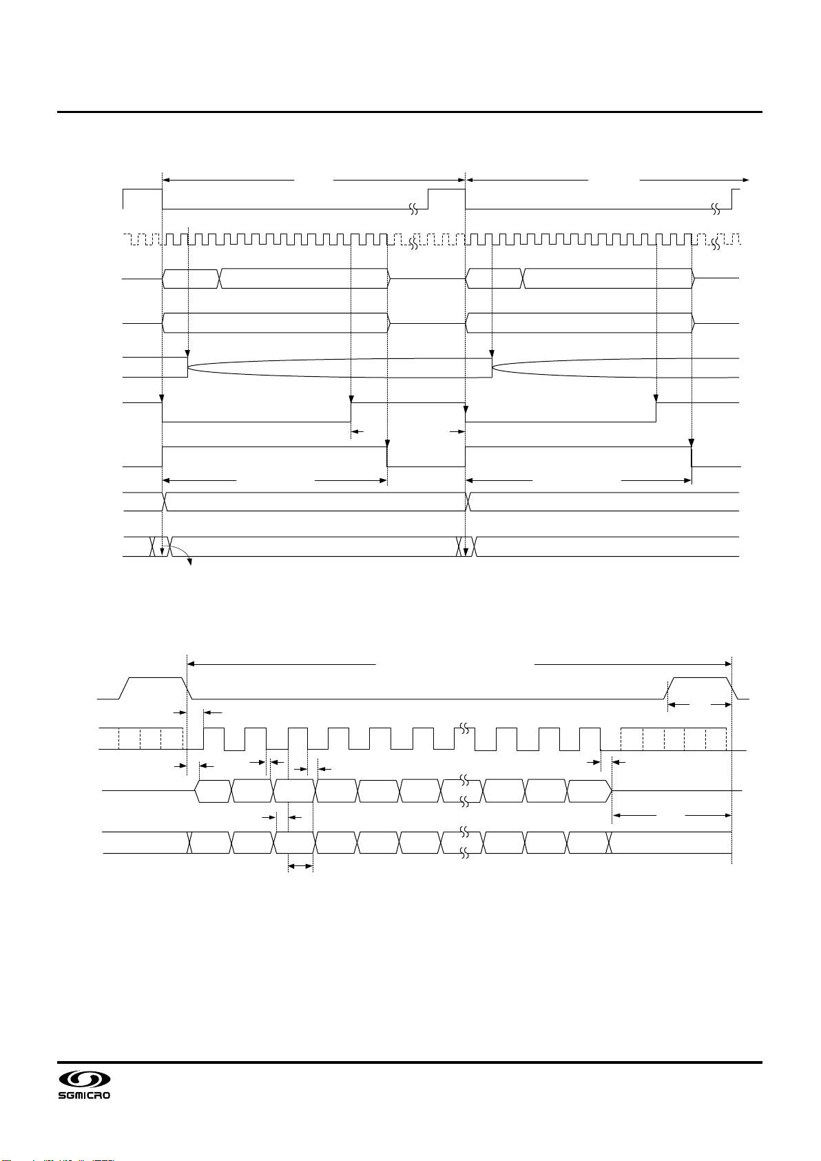
TIMING DIAGRAM
nCS
SCLK
SDO
SDI
MUX
Acquisition
Conversion
GPO
GPI
GPI status is latched on the falling edge of
nCS and transferred to the SDO frame n
Frame n Frame (n+1)
Top 4 Bits 12-Bit Conversion Result
16-Bit I/P Word
Mux Chan Change
Analog I/P Setting after Chan Change
Sampling Instance
Acquisition Phase t
ACQ
Conversion Phase Conversion Phase t
CNV
Data Written (through SDI) in Frame (n-1) Data Written (through SDI) in Frame n
1 3 5 7 9 11 13 16 1 3 5 7 9 11 13 161515
Top 4 Bits 12-Bit Conversion Result
Mux Chan Change
16-Bit I/P Word
Figure 1. Device Operation Timing Diagram
nCS
SCLK
SDO
SDI
1/t Throughput (Single Frame)
a
tSU1
tD1 tH1 tD2
tD3
tSU2
tH2
tQ
tW1
1 2 3 4 5 6 14 15 16
DO15 DO14 DO13 DO12 DO11
MSB
DO10
MSB-1
DO2
LSB+2
DO1
LSB+1
DO0
LSB
DI15 DI14 DI13 DI12 DI11 DI10 DI2 DI1 DI0
Figure 2. Serial Interface Timing Diagram
12-Bit, 1MSPS, 16 Channels,
SGM5200 Single-Ended, Serial Interface ADC
9
SEPTEMBER 2021
SG Micro Corp
www.sg-micro.com
TYPICAL PERFORMANCE CHARACTERISTICS
Signal-to-Noise Ratio vs. Supply Voltage (Range 1)
Signal-to-Noise Ratio vs. Supply Voltage (Range 2)
Signal-to-Noise + Distortion vs. Supply Voltage (Range 1)
Signal-to-Noise + Distortion vs. Supply Voltage (Range 2)
Total Harmonic Distortion vs. Supply Voltage (Range 1)
Total Harmonic Distortion vs. Supply Voltage (Range 2)
65
66
67
68
69
70
71
2.7 3.1 3.5 3.9 4.3 4.7 5.1 5.5
Signal-to-Noise Ratio (dB)
Supply Voltage (V)
VBD = 3V, fS= 1MSPS,
fIN = 100kHz, TA= +25℃
67
68
69
70
71
72
73
5.0 5.1 5.2 5.3 5.4 5.5
Signal-to-Noise Ratio (dB)
Supply Voltage (V)
VBD = 3V, fS= 1MSPS,
fIN = 100kHz, TA= +25℃
63
64
65
66
67
68
69
2.7 3.1 3.5 3.9 4.3 4.7 5.1 5.5
Signal-to-
Noise Ratio + Distortion (dB)
Supply Voltage (V)
VBD = 3V, fS= 1MSPS,
fIN = 100kHz, TA= +25℃
66
67
68
69
70
71
72
5.0 5.1 5.2 5.3 5.4 5.5
Signal-to-
Noise Ratio + Distortion (dB)
Supply Voltage (V)
VBD = 3V, fS= 1MSPS,
fIN = 100kHz, TA= +25℃
-77
-76
-75
-74
-73
-72
-71
2.7 3.1 3.5 3.9 4.3 4.7 5.1 5.5
Total Harmonic Distortion (dB)
Supply Voltage (V)
VBD = 3V, fS= 1MSPS,
fIN = 100kHz, TA= +25℃
-79
-78
-77
-76
-75
-74
-73
5.0 5.1 5.2 5.3 5.4 5.5
Total Harmonic Distortion (dB)
Supply Voltage (V)
VBD = 3V, fS= 1MSPS,
fIN = 100kHz, TA= +25℃

12-Bit, 1MSPS, 16 Channels,
SGM5200 Single-Ended, Serial Interface ADC
10
SEPTEMBER 2021
SG Micro Corp
www.sg-micro.com
TYPICAL PERFORMANCE CHARACTERISTICS (continued)
Spurious Free Dynamic Range vs. Supply Voltage (Range 1)
Spurious Free Dynamic Range vs. Supply Voltage (Range 2)
Signal-to-Noise Ratio vs. Input Frequency
Signal-to-Noise + Distortion vs. Input Frequency
Total Harmonic Distortion vs. Input Frequency
Spurious Free Dynamic Range vs. Input Frequency
72
73
74
75
76
77
78
2.7 3.1 3.5 3.9 4.3 4.7 5.1 5.5
Spurious Free Dynamic Range (dB)
Supply Voltage (V)
VBD = 3V, fS= 1MSPS,
fIN = 100kHz, TA= +25℃
74
75
76
77
78
79
80
5.0 5.1 5.2 5.3 5.4 5.5
Spurious Free Dynamic Range (dB)
Supply Voltage (V)
VBD = 3V, fS= 1MSPS,
fIN = 100kHz, TA= +25℃
67
68
69
70
71
72
73
10 30 50 70 90 110 130 150
Signal-to-Noise Ratio (dB)
Input Frequency (kHz)
VA= 5V, VBD = 3V,
fS= 1MSPS, TA= +25℃,
MXO Shorted to AINP
66
67
68
69
70
71
72
10 30 50 70 90 110 130 150
Signal-to-Noise + Distortion (dB)
Input Frequency (kHz)
VA= 5V, VBD = 3V,
fS= 1MSPS, TA= +25℃,
MXO Shorted to AINP
-81
-79
-77
-75
-73
-71
-69
10 30 50 70 90 110 130 150
Total Harmonic Distortion (dB)
Input Frequency (kHz)
VA= 5V, VBD = 3V,
fS= 1MSPS, TA= +25℃,
MXO Shorted to AINP
73
75
77
79
81
83
85
10 30 50 70 90 110 130 150
Spurious Free Dynamic Range (dB)
Input Frequency (kHz)
VA= 5V, VBD = 3V,
fS= 1MSPS, TA= +25℃,
MXO Shorted to AINP

12-Bit, 1MSPS, 16 Channels,
SGM5200 Single-Ended, Serial Interface ADC
11
SEPTEMBER 2021
SG Micro Corp
www.sg-micro.com
TYPICAL PERFORMANCE CHARACTERISTICS (continued)
Signal-to-Noise Ratio vs. Temperature
Signal-to-Noise + Distortion vs. Temperature
Total Harmonic Distortion vs. Temperature
Spurious Free Dynamic Range vs. Temperature
Differential Nonlinearity Variation Across Channels
Integral Nonlinearity Variation Across Channels
68.5
69.0
69.5
70.0
70.5
71.0
71.5
-50 -25 025 50 75 100 125 150
Signal-to-Noise Ratio (dB)
Temperature (℃)
VA= 5V, VBD = 3V,
fS= 1MSPS, fIN = 100kHz
66
67
68
69
70
71
72
-50 -25 025 50 75 100 125 150
Signal-to-Noise + Distortion (dB)
Temperature (℃)
VA= 5V, VBD = 3V,
fS= 1MSPS, fIN = 100kHz
-78
-77
-76
-75
-74
-73
-72
-50 -25 025 50 75 100 125 150
Total Harmonic Distortion (dB)
Temperature (℃)
VA= 5V, VBD = 3V,
fS= 1MSPS, fIN = 100kHz
75
76
77
78
79
80
81
-50 -25 025 50 75 100 125 150
Spurious Free Dynamic Range (dB)
Temperature (℃)
VA= 5V, VBD = 3V,
fS= 1MSPS, fIN = 100kHz
-1.0
-0.8
-0.6
-0.4
-0.2
0.0
0.2
0.4
0.6
0.8
1.0
012345678910 11 12 13 14 15
Differential Nonlinearity (LSBs)
Channel Number
VA= 5V, VBD = 5V, fS= 1MSPS
DNL MAX
DNL MIN
-1.0
-0.8
-0.6
-0.4
-0.2
0.0
0.2
0.4
0.6
0.8
1.0
012345678910 11 12 13 14 15
Integral Nonlinearity (LSB)
Channel Number
VA= 5V, VBD = 5V, fS= 1MSPS
INL MAX
INL MIN

12-Bit, 1MSPS, 16 Channels,
SGM5200 Single-Ended, Serial Interface ADC
12
SEPTEMBER 2021
SG Micro Corp
www.sg-micro.com
TYPICAL PERFORMANCE CHARACTERISTICS (continued)
Gain Error Variation Across Channels
Offset Error Variation Across Channels
Signal-to-Noise Ratio Variation Across Channels
Signal-to-Noise + Distortion Variation Across Channels
Crosstalk vs. Input Frequency
Input Leakage Current vs. Temperature
-1.0
-0.8
-0.6
-0.4
-0.2
0.0
0.2
0.4
0.6
0.8
1.0
012345678910 11 12 13 14 15
Gain Error (LSB)
Channel Number
VA= 5V, VBD = 5V, fS= 1MSPS
-1.0
-0.8
-0.6
-0.4
-0.2
0.0
0.2
0.4
0.6
0.8
1.0
012345678910 11 12 13 14 15
Offset Error (LSB)
Channel Number
VA= 5V, VBD = 5V, fS= 1MSPS
66.0
66.5
67.0
67.5
68.0
68.5
69.0
69.5
70.0
70.5
71.0
012345678910 11 12 13 14 15
Signal-to-Noise Ratio (dB)
Channel Number
VA= 5V, VBD = 5V, fS= 1MSPS
65.0
65.5
66.0
66.5
67.0
67.5
68.0
68.5
69.0
69.5
70.0
012345678910 11 12 13 14 15
Signal-to-Noise + Distortion (dB)
Channel Number
VA= 5V, VBD = 5V, fS= 1MSPS
0
20
40
60
80
100
120
050 100 150 200 250
Crosstalk (dB)
Input Frequency (kHz)
VA= 5V, VBD = 5V,
fS= 1MSPS, CH0, CH1
Isolation
Memory
-2
18
38
58
78
98
-50 -25 025 50 75 100 125 150
Input Leakage Current (nA)
Temperature (℃)
VA= 5V, VBD = 5V
VINP = 2.5V
VINP = 1.25V
VINP = 0.12V

12-Bit, 1MSPS, 16 Channels,
SGM5200 Single-Ended, Serial Interface ADC
13
SEPTEMBER 2021
SG Micro Corp
www.sg-micro.com
TYPICAL PERFORMANCE CHARACTERISTICS (continued)
Gain Error vs. Temperature (Range 1)
Gain Error vs. Temperature (Range 2)
Offset Error vs. Temperature (Range 1)
Offset Error vs. Temperature (Range 2)
Total Unadjusted Error (TUE Maximum) (Range 1)
Total Unadjusted Error (TUE Maximum) (Range 2)
-1.5
-1.0
-0.5
0.0
0.5
1.0
1.5
2.0
-50 -25 025 50 75 100 125 150
Gain Error (LSB)
Temperature (℃)
VA= 5.5V, VBD = 1.8V, fS= 1MSPS
-1.0
-0.5
0.0
0.5
1.0
1.5
2.0
2.5
-50 -25 025 50 75 100 125 150
Gain Error (LSB)
Temperature (℃)
VA= 5.5V, VBD = 1.8V, fS= 1MSPS
-0.8
-0.6
-0.4
-0.2
0.0
0.2
0.4
0.6
-50 -25 025 50 75 100 125 150
Offset Error (LSB)
Temperature (℃)
VA= 5.5V, VBD = 1.8V, fS= 1MSPS
-0.6
-0.4
-0.2
0.0
0.2
0.4
0.6
0.8
-50 -25 025 50 75 100 125 150
Offset Error (LSB)
Temperature (℃)
VA= 5.5V, VBD = 1.8V, fS= 1MSPS
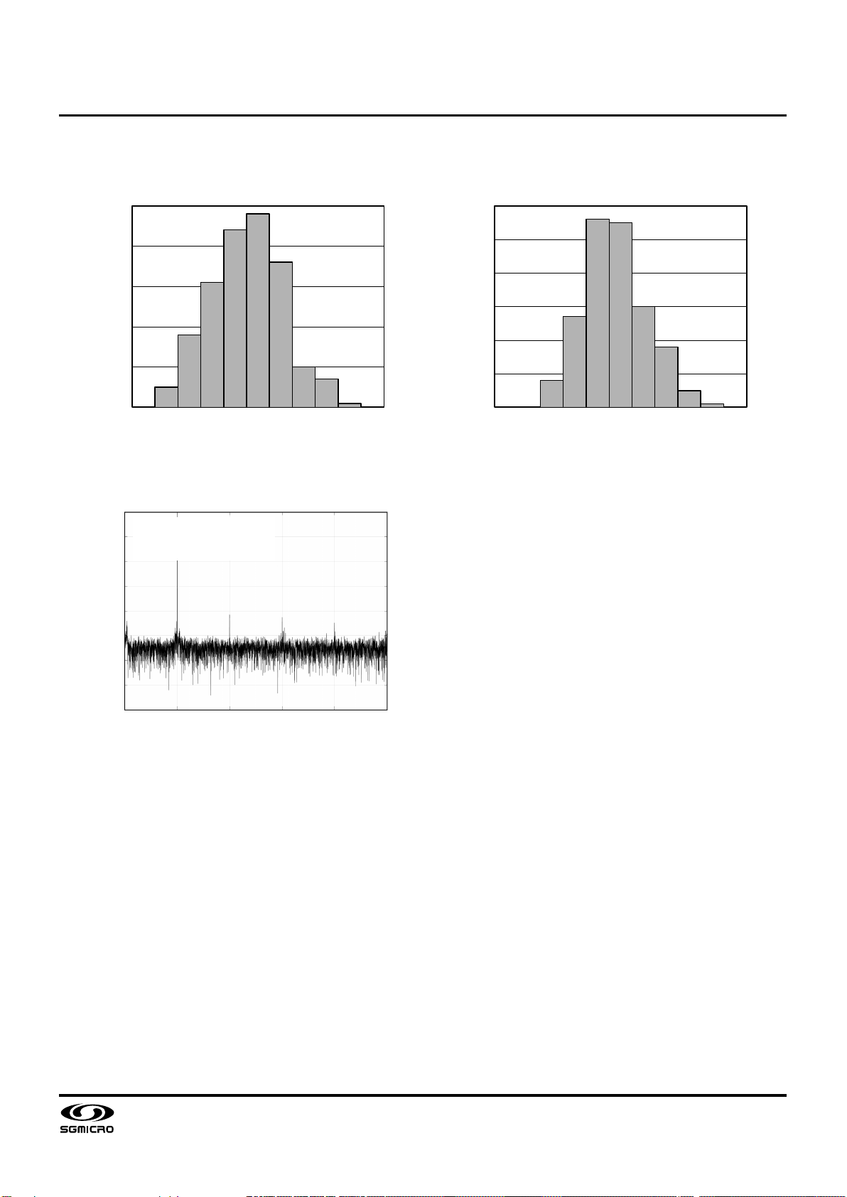
0
5
10
15
20
25
30
35
0.95
1
1.05
1.1
1.15
1.2
1.25
1.3
1.35
1.4
1.45
Percentage of Devices (%)
TUE MAX (LSB)
0
5
10
15
20
25
30
1.3
1.4
1.5
1.6
1.7
1.8
1.9
2
2.1
2.2
2.3
2.4
2.5
Percentage of Devices (%)
TUE MAX (LSB)
12-Bit, 1MSPS, 16 Channels,
SGM5200 Single-Ended, Serial Interface ADC
14
SEPTEMBER 2021
SG Micro Corp
www.sg-micro.com
TYPICAL PERFORMANCE CHARACTERISTICS (continued)
Total Unadjusted Error (TUE Minimum) (Range 1)
Total Unadjusted Error (TUE Minimum) (Range 2)
Typical FFT Plot
Amplitude (dB)
0
-20
-40
-60
-80
-100
-120
-140
-160
0
100 200 300 400 500
Frequency (kHz)
0
5
10
15
20
25
-2
-1.95
-1.9
-1.85
-1.8
-1.75
-1.7
-1.65
-1.6
-1.55
-1.5
Percentage of Devices (%)
TUE MIN (LSB)
0
5
10
15
20
25
30
-2.35
-2.25
-2.15
-2.05
-1.95
-1.85
-1.75
-1.65
-1.55
-1.45
-1.35
Percentage of Devices (%)
TUE MIN (LSB)
V
A
= 5V, V
BD
= 5V,
fS= 1MSPS, fIN = 100kHz,
Npoints = 16384
12-Bit, 1MSPS, 16 Channels,
SGM5200 Single-Ended, Serial Interface ADC
15
SEPTEMBER 2021
SG Micro Corp
www.sg-micro.com
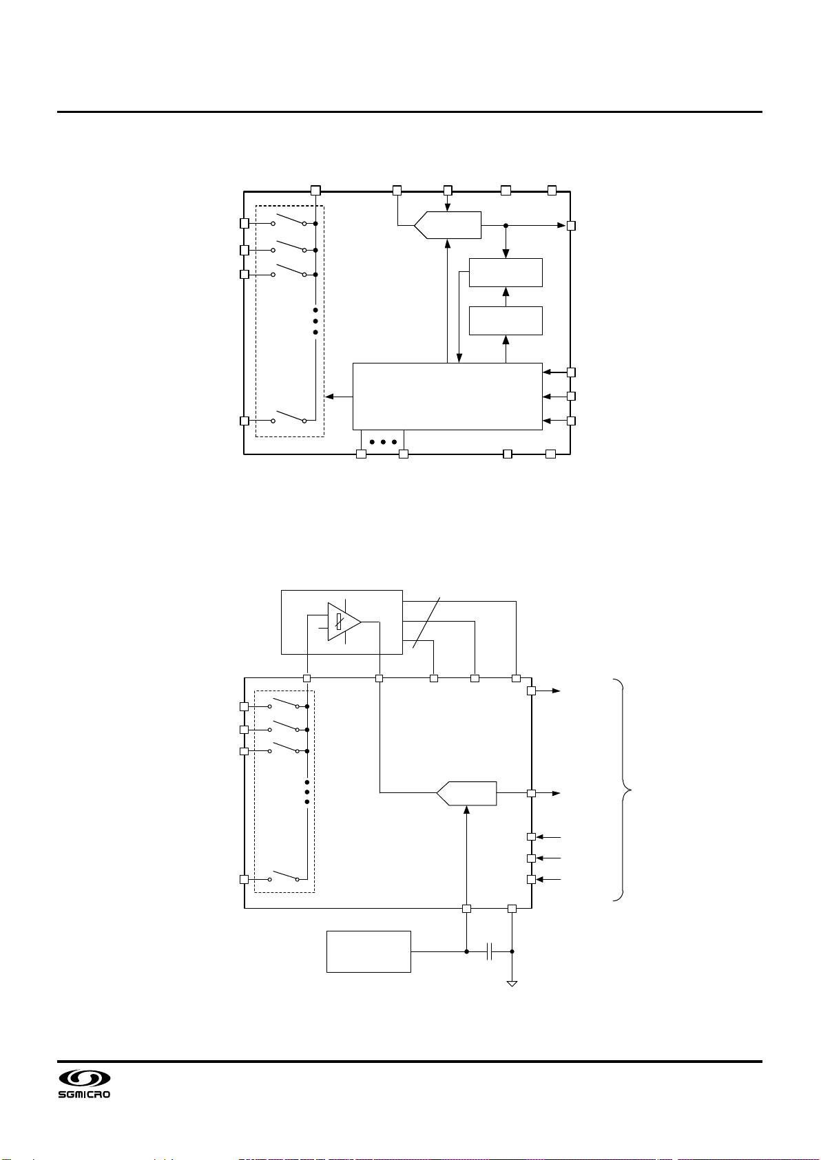
FUNCTIONAL BLOCK DIAGRAM
ADC
Control Logic
&
Sequencing
SDO
SDI
SCLK
nCS
+VBD
CH15
CH2
CH1
CH0
MXO AINP REFP +VA AGND
Alarm
Threshold
Compare
GPIO0 GPIO3
(1)
BDGND
NOTE:
1. There are 4 GPIOs in TSSOP package and 1 GPIO in TQFN package.
Figure 3. Block Diagram
TYPICAL APPLICATION CIRCUITS
ADC
REF
SGM4029-2.5
High Input Impedance PGA
(or Non-Inverting Buffer
Such as SGM8604-1)
GPIO0
SDO
SDI
SCLK
nCS
REFP
O/P
CH15
CH2
CH1
CH0
MXO AINP GPIO1 GPIO2 GPIO3
PGA Gain Control
High-Alarm
Low-Alarm
To Host
REFM
10μF
Figure 4. Typical Application Circuit

12-Bit, 1MSPS, 16 Channels,
SGM5200 Single-Ended, Serial Interface ADC
16
SEPTEMBER 2021
SG Micro Corp
www.sg-micro.com
DETAILED DESCRIPTION
Overview
The SGM5200 is a 12-bit, high-speed, low-power and
successive approximation register (SAR) analog-to-digital
converter (ADC) that uses an external reference. The
architecture is based on charge redistribution, which
inherently includes a sample/hold function. The analog
inputs to the SGM5200 are provided to CHx input channels.
All input channels share a common analog ground AGND.
The SGM5200 has multiplexer breakout feature which
allows user to connect the signal conditioning circuit
between multiplexer output (MXO) and ADC input (AINP).
This feature enables use of common signal conditioning
block for the input signal which exhibit similar performance
characteristics. SGM5200 can be programmed to select a
channel manually or can be programmed into the auto
channel select mode to sweep through the input channels
automatically.
Figure 1 and Figure 2 show device operation timing. Device
operation is controlled with nCS, SCLK and SDI. The device
outputs its data on SDO.
Each frame begins with the falling edge of nCS. With the
falling edge of nCS, the input signal from the selected
channel is sampled and the conversion process is initiated.
The device outputs data while the conversion is in progress.
The 16-bit data word contains a 4-bit channel address,
followed by a 12-bit conversion result in MSB first format.
There is an option to read the GPIO status instead of the
channel address. (Refer to Table 1, Table 2 and Table 5 for
more details.)
The device selects a new multiplexer channel on the 2nd
SCLK falling edge. The acquisition phase starts on the 14th
SCLK rising edge. On the next nCS falling edge, the
acquisition phase will end and the device starts a new
frame.
The TSSOP packaged device has four general purpose IO
(GPIO0 - GPIO3) pins while TQFN version has only one
GPIO0 pin. The four pins can be individually programmed
as GPO or GPI. It is also possible to use them for
pre-assigned functions, refer to Table 9. GPO data can be
written into the device through the SDI line. The device
refreshes the GPO data on the nCS falling edge as per the
SDI data written in previous frame.
Similarly the device latches GPI status on the nCS falling
edge and outputs the GPI data on the SDO line (if GPI read
is enabled by writing DI4 = 1 in the previous frame) in the
same frame starting with the nCS falling edge.
The falling edge of nCS clocks out DO15 (the first bit of the
4-bit channel address) and remaining address bits are
clocked out on every falling edge of SCLK until the third
falling edge. The conversion result MSB is clocked out on
the 4th SCLK falling edge and LSB on the 15th falling edge
respectively for 12-bit. On the 16th falling edge of SCLK,
SDO goes to the 3-state condition. The conversion ends on
the 16th falling edge of SCLK. The nCS can be asserted
(pulled high) only after 16 clocks have elapsed.
The device reads a 16-bit word on the SDI pin while it
outputs the data on the SDO pin. SDI data is latched on
every rising edge of SCLK starting with the 1st clock as
shown in Figure 2. nCS can be asserted (pulled high) only
after 16 clocks have elapsed.
The device has two (high and low) programmable alarm
thresholds per channel. If the input crosses these limits, the
device flags out an alarm on GPIO0/GPIO1 depending on
the GPIO program register settings (refer to Table 9). The
alarm is asserted (under the alarm conditions) on the 12th
falling edge of SCLK in the same frame when a data
conversion is in progress. The alarm output is reset on the
10th falling edge of SCLK in the next frame.
Reference
The SGM5200 can operate with an external 2.5V ± 10mV
reference. A clean, low noise and well-decoupled
reference voltage on the REFP pin is required to ensure
good performance of the converter. A low noise bandgap
reference can be used to drive this pin. A 10μF ceramic
decoupling capacitor is required between the REFP and
REFM pins of the converter. The capacitor should be
placed as close as possible to the pins of the device.
Power Saving
The SGM5200 offers a power-down feature to save power
when not in use. There are two ways to power down the
device. It can be powered down by writing DI5 = 1 in the
mode control register (refer to Table 1, Table 2and Table 5);
in this case, the device powers down on the 16th falling
edge of SCLK in the next data frame. Another way to power
down the device is through GPIO. GPIO3 can act as the
nPD input (refer to Table 9, for assigning this functionality to
GPIO3). This is an asynchronous and active low input. The
device powers down instantaneously after GPIO3 (nPD) = 0.
The device will power up again on the nCS falling edge
while DI5 = 0 in the mode control register and GPIO3 (nPD)
= 1.

12-Bit, 1MSPS, 16 Channels,
SGM5200 Single-Ended, Serial Interface ADC
17
SEPTEMBER 2021
SG Micro Corp
www.sg-micro.com
DETAILED DESCRIPTION (continued)
Device Functional Modes
Channel Sequencing Modes
There are three modes for channel sequencing, namely
manual mode, auto-1 mode and auto-2 mode. Mode
selection is done by writing into the mode control register
(refer to Table 1, Table 2 and Table 5). A new multiplexer
channel is selected on the 2nd falling edge of SCLK (as
shown in Figure 1) in all three modes.
Manual Mode
When configured to operate in manual mode, the next
channel to be selected is programmed in each frame and
the device selects the programmed channel in the next
frame. On power-up or after reset the default channel is
'channel 0' and the device is in manual mode.
Auto-1 Mode
In this mode, the device scans pre-programmed channels in
ascending order. A new multiplexer channel is selected
every frame on the 2nd falling edge of SCLK. There is a
separate program register for pre-programming the channel
sequence. Table 3 and Ta b l e 4 show auto-1 program
register settings.
Once programmed the device retains program register
settings until the device is powered down, reset or
reprogrammed. It is allowed to exit and re-enter the auto-1
mode any number of times without disturbing program
register settings.
The auto-1 program register is reset to "FFFF" hex for
SGM5200 upon device power-up or reset; implying the
device scans all channels in ascending order.
Auto-2 Mode
In this mode, the user can configure the program register to
select the last channel in the scan sequence. The device
scans all channels from channel 0 up to and including the
last channel in ascending order. The multiplexer channel is
selected every frame on the 2nd falling edge of SCLK. There
is a separate program register for preprogramming of the
last channel in the sequence (multiplexer depth). Table 6
lists the auto-2 program register settings for selection of the
last channel in the sequence.
Once programmed the device retains program register
settings until the device is powered down, reset or
reprogrammed. It is allowed to exit and re-enter the auto-2
mode any number of times without disturbing program
register settings.
On power-up or reset the bits DI[9:6] of the auto-2 program
register are reset to "F" hex for SGM5200; implying the
device scans all channels in ascending order.
Device Programming and Mode Control
The following section describes device programming and
mode control. The device features two types of registers to
configure and operate the device in different modes. These
registers are referred as configuration registers. There are
two types of configuration registers namely mode control
register and program registers.
Mode Control Register
A mode control register is configured to operate the device
in one of three channel sequencing modes, namely manual
mode, auto-1 mode and auto-2 mode. It is also used to
control user programmable features like range selection,
device power-down control. GPIO read control and writing
output data into the GPIO.
Program Registers
The program registers are used for device configuration
settings and are typically programmed once on power-up
or after device reset. There are different program registers
such as auto-1 mode programming for preprogramming the
channel sequence, auto-2 mode programming for selection
of the last channel in the sequence, alarm programming for
all 16 channels and GPIO for individual pin configuration as
GPI or GPO or a pre-assigned function.
Device Power-Up Sequence
The device power-up sequence is shown in Figure 5. By
default, the mode control register is configured for manual
mode and the default channel is channel 0. As explained
previously, the device offers program registers to
configure user programmable features like GPIOs, Alarms
and to preprogram the channel sequence for auto modes.
At 'power-up or on reset', these registers are set to the
default values listed in Table 1 to Table 9. On power-up or
after reset, it is required to program mode control register
and program registers to required mode of operation. Once
configured, the device is ready to use in any of the three
channel sequencing modes namely manual, auto-1 and
auto-2.

12-Bit, 1MSPS, 16 Channels,
SGM5200 Single-Ended, Serial Interface ADC
18
SEPTEMBER 2021
SG Micro Corp
www.sg-micro.com
DETAILED DESCRIPTION (continued)
nCS
First Frame
Device operation in manual mode, channel 0;
SDO invalid in first frame
Auto-1 register program
(1)
Device power-up or reset
Auto-2 register program
(1)
nCS
nCS
Alarm register program
(1)
GPIO register program
(1)
nCS
nCS
Operation in manual mode
Operation in auto-1 mode Operation in auto-2 mode
nCS
nCS nCS
NOTES:
1. The device continues its operation in manual mode channel 0 throughout the programming sequence and outputs valid
conversion results. It is possible to change channel, range, GPIO by inserting extra frames in between two programming blocks.
It is also possible to bypass any programming block if the user does not intend to use that feature.
2. It is possible to reprogram the device at any time during operation, regardless of what mode the device is in. During
programming the device continues its operation in whatever mode it is in and outputs valid data.
Figure 5. Device Power-Up Sequence
12-Bit, 1MSPS, 16 Channels,
SGM5200 Single-Ended, Serial Interface ADC
19
SEPTEMBER 2021
SG Micro Corp
www.sg-micro.com
DETAILED DESCRIPTION (continued)
Operating in Manual Mode
Figure 6 illustrates the steps involved in operating in manual channel sequencing mode. Table 1 lists the mode control register
settings for manual mode. There are no program registers in manual mode.
nCS
Frame: n-1
Device operation in auto-1 or auto-2 mode
nCS
Frame: n
Request for
Manual Mode
*Sample: Samples and converts channel selected in 'frame (n-1)'.
*MUX: Selects channel incremented from previous frame as per auto sequence. This channel will be
acquired in this frame and sampled at start of 'frame (n+1)'.
*Range: As programmed in 'frame (n-1)'. Applies to channel selected for acquisition in current frame.
*SDI: Programming for 'frame (n+1)'.
DI[15:12] = 0001 (binary). Selects manual mode.
DI11 = 1 enables programming of 'range and GPIO'.
DI[10:7] = Binary address of the next channel.
DI6 as per required range for channel to be selected.
DI5 = 0. No power-down.
DI[4:0] as per GPIO settings.
*SDO: DO[15:0] address (or GPIO data) & conversion data of channel selected in 'frame (n-1)'.
*GPIO:
O/P: Latched on nCS falling edge as per DI[3:0] written in 'frame (n-1)'.
I/P: Input status latched on falling edge of nCS and transferred serially on SDO in the same frame.
Change to manual mode?
Yes
No
nCS
Frame: n+1
Entry into
Manual Mode
*Sample: Samples and converts channel selected in 'frame n'.
*MUX: Selects channel programmed in 'frame n' (manual mode). This channel will be acquired in this
frame and sampled at start of 'frame (n+2)'.
*Range: As programmed in 'frame n'. Applies to channel selected for acquisition in current frame.
*SDI: Programming for 'frame (n+2)'.
DI[15:12] = 0001 (binary).To continue in manual mode.
DI11 = 1 enables programming of 'range and GPIO'.
DI[10:7] = Binary address of the next channel.
DI6 as per required range for channel to be selected.
DI5 = 0. No power-down.
DI[4:0] as per GPIO settings.
*SDO: DO[15:0] address (or GPIO data) & conversion data of channel selected in 'frame n'.
*GPIO:
O/P: Latched on nCS falling edge as per DI[3:0] written in 'frame n'.
I/P: Input status latched on falling edge of nCS and transferred serially on SDO in the same frame.
nCS
Frame: n+2
Operation in
Manual Mode
*Sample: Samples and converts channel selected in 'frame (n+1)'.
*MUX: Selects channel programmed in 'frame (n+1)' (manual mode). This channel will be acquired in
this frame and sampled at start of 'frame n+3'.
*Range: As programmed in 'frame (n+1)'. Applies to channel selected for acquisition in current frame.
*SDI: Programming for 'frame (n+3)'.
DI[15:12] = 0001 (binary). Selects manual mode.
DI11 = 1 enables programming of 'range and GPIO'.
DI[10:7] = Binary address of the next channel.
DI6 as per required range for channel to be selected.
DI5 = 0. No power-down.
DI[4:0] as per GPIO settings.
*SDO: DO[15:0] address (or GPIO data) & conversion data of channel selected in 'frame (n+1)'.
*GPIO:
O/P: Latched on nCS falling edge as per DI[3:0] written in 'frame (n+1)'.
I/P: Input status latched on falling edge of nCS and transferred serially on SDO in the same frame.
nCS Continue operation in manual mode
Figure 6. Entering and Running in Manual Channel Sequencing Mode
12-Bit, 1MSPS, 16 Channels,
SGM5200 Single-Ended, Serial Interface ADC
20
SEPTEMBER 2021
SG Micro Corp
www.sg-micro.com
DETAILED DESCRIPTION (continued)
Table 1. Mode Control Register Settings for Manual Mode
Bits
Reset
State
Logic
State
Function
DI[15:12] 0001 0001 Selects manual mode.
DI11 0 1 Enables programming of bits DI[6:0].
0 Device retains values of DI[6:0] from the previous frame.
DI[10:7] 0000
This 4-bit data represents the address of the next channel to be selected in the next frame.
DI10: MSB and DI7: LSB. For example, 0000 represents channel 0, 0001 represents channel 1
and so
forth.
DI6 0 0 Selects 0V to VREF input range (Range 1).
1 Selects 0V to 2 × VREF input range (Range 2).
DI5 0 0 Device normal operation (no power-down).
1 Device powers down on the 16
th
SCLK falling edge.
DI4 0
0
SDO outputs current channel address of the channel on DO[15:12] followed by 12-bit conversion result
on DO[11:0].
1
GPIO3 - GPIO0 data (both input and output) is mapped onto DO[15:12] in the order shown below. Lower
data bits DO[11:0] represent 12-bit conversion result of the current channel.
DO15 DO14 DO13 DO12
GPIO3
(1)
GPIO2
(1)
GPIO1
(1)
GPIO0
(1)
DI[3:0] 0000
GPIO data for the channels configured as output. Device will ignore the data for the channel which is
configured as input. SDI bit and corresponding GPIO information is given below.
DI3 DI2 DI1 DI0
GPIO3 (1) GPIO2 (1) GPIO1 (1) GPIO0 (1)
NOTE: 1. GPIO1 to GPIO3 are available only in TSSOP packaged device. TQFN device offers GPIO0 only.
Figure 7 shows an example in which manual mode is used
to scan channels 4, 7 and 9. The command to select
channel 4 (CH4) is issued in the nth frame and the data
corresponding to CH4 is available in the (n+2)th frame.
Internally, the SDI command is parsed and on the rising
edge of nCS of the (n+1)th frame and the MUX switches
accordingly on the 2nd falling edge of SCLK in this frame.
On the rising edge of nCS of the (n+2)th frame, the input
signal for CH4 is sampled and the ADC sends the
conversion data in this third frame. The device follows the
same steps and the ADC sends the conversion data for
CH7 and CH9 in the subsequent two frames.
nCS
SCLK
SDO
SDI
Frame n Frame (n+1) Frame (n+2)
Sample
CHx
Sample
CHy
Sample
CH4
Sample
CH7
Select CH4 Select CH7 Select CH9
Data CHx Data CHy Data CH4
t
CYCLE
Figure 7. Example Manual Mode Timing Diagram
Table of contents


 user guide")


