*
Maximum
power
output
of:
50
watts
per
channel
with
a
4-speaker
system,
40
watts
x
2
plus
140
watts
x
1
with
a
3-speaker
system
or
120
watts
per
channel
with
a
2-speaker
system
(at
4
ohms).
¢Wide
dynamic
range
and
low
distortion
(less
than
0.005%).
¢
Provided
with
a
protection
circuit.
*
Pulse
power
supply”
forstable
and
regulated
output
power.
¢
Direct
connection
can
be
made
with
the
speaker
output
of
your
car
audio
if
it
is
not
equipped
with
the
line
outputs
(High
level
input
connection).
*Pulse
power
supply
This
unit
has
a
built-in
convertor
which
converts
the
power
supply
from
the
DC
12
volt
car
battery
into
high
speed
signals
by
the
use
of
the
semiconductor
switch.
These
signals
will
be
stepped
up
by
the
built-in
pulse
transformer
and
separated
into
both
positive
and
negative
power
supplies
before’
being
converted
into
the
direct
current
again.
This
is
to
regulate
the
otherwise
variable
voltage
of
the
car
battery.
The
light
weight
power
supply
system
provides
the
highly
efficient
power
supply
with
a
low
impedance
ouiput.
TABLE
OF
CONTENTS
Section
Title
Page
1.
GENERAL
oon
sssssscssessssescesesessseseaseneens
3
2.
DIAGRAMS
2-1.
Block
Diagram
wii
eeessssceseceesscssceeeetecnecessesenseeeteensenssaseasees
5
2-2.
Printed
Wiring
Boards.
cccsscsseceeeereseesssessseseessseseseees
7
2-3.
Schematic
Diagram,
.......cccccccccsssscsssosoessensosvessscsssoesstasesecesageenens
9
2-4.
Semiconductor
Lead
Layouts
wc
seseeeeseseeteeeeereeseeees
11
3.
EXPLODED:
VIEW
|.
ccsoiaitnaa
hibuingucmialamers:
12
4.
ELECTRICAL
PARTS
LIST
ee
13
Fuse
Replacement
If
the
fuse
blows,
check
the
power
connection
and
replace
the
fuse.
If
the
fuse
blows
again
after
the
replacement,
there
may
be
an
internal
malfunction.
In
such
a
case,
consult
your
nearest
Sony
dealer.
Warning
Use
the
specified
fuse
with
correct
amperage
rating.
Use
of a
fuse
with
higher
amperage
rating
may
cause
serious
damage
to
the
unit.
*Protection
circuit
This
amplifier
is
provided
with
a
protection
circuit
which
operates
in
the
following
cases
“when:
~~
the
unit
is
overheated
~~
a
DC
current
is
generated
—
the
speaker
terminals
are
short
circuited.
The
color
of
the
POWER/PROTECTOR
indicator
will
change
from
green
to
red
and
the
unit
will
shut
down.
If
this
happens,
turn
off
the
connected
equipment
and
take
out
the
cassette
tape
or
disc
and
determine
the
cause
of
the
malfunction.
If
the
amplifier
has
overheated,
wait
until
the
unit
cools
off.
POWER/PROTECTOR
indicator
SERVICE
NOTE
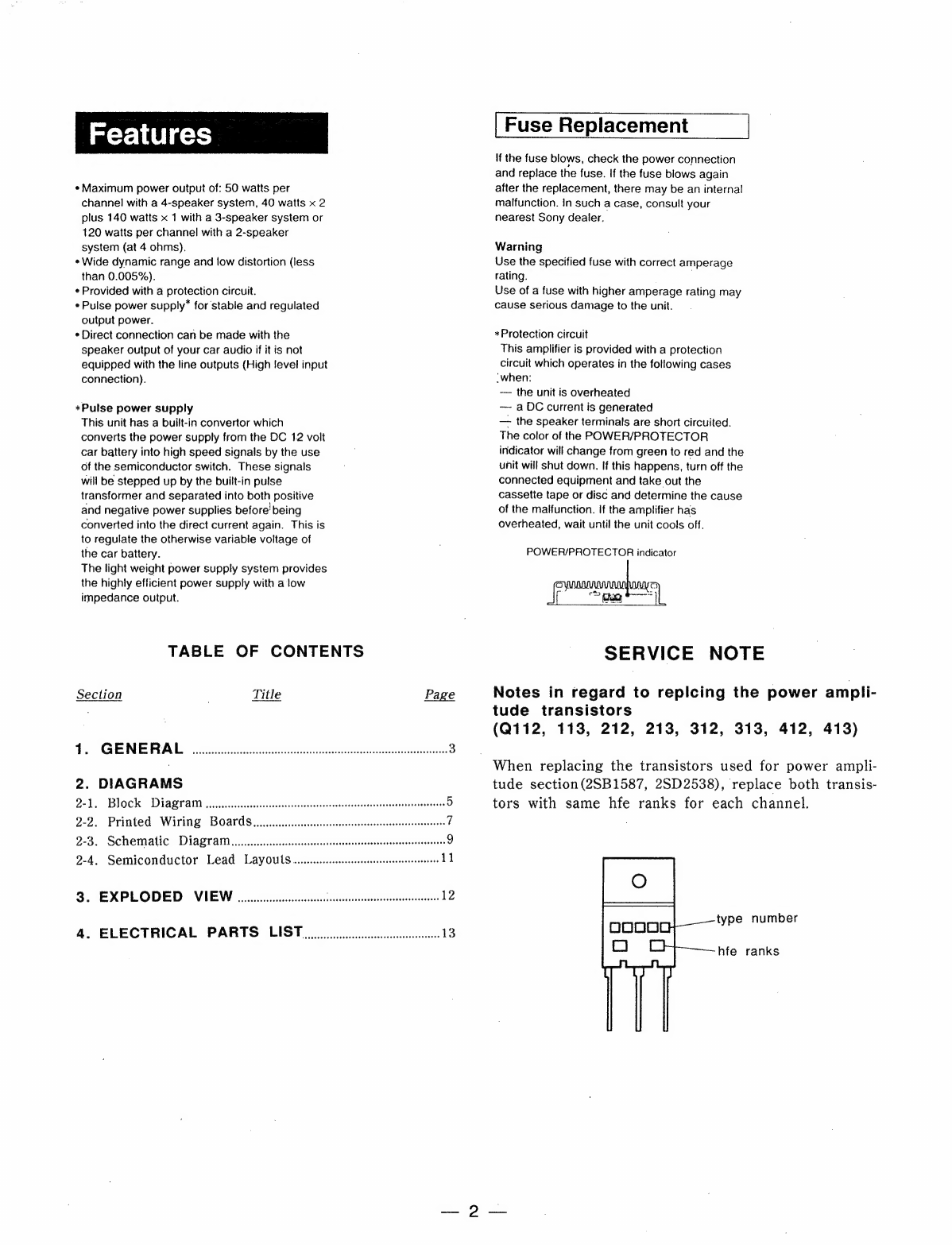
Notes
in
regard
to
replcing
the
power
ampli-
tude
transistors
(Q112,
113,
212,
213, 312, 313,
412,
413)
When
replacing
the
transistors
used
for
power
ampli-
tude
section
(25B1587,
25D2538),
replace
both
transis-
tors
with
same
hfe
ranks
for
each
channel.
type
number
hfe
ranks