– 20 –
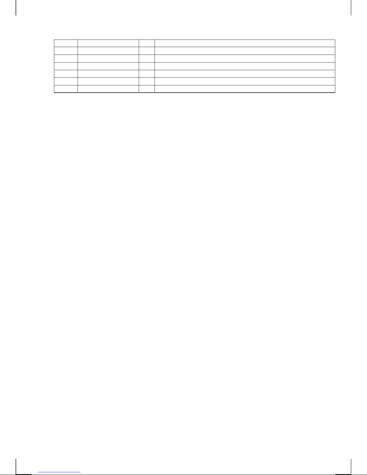
Pin No. Pin Name I/O Pin Description
53 ASY.O O EFM full-swing output (“L” : VSS, “H” : VDD)
54 VC I Center voltage input
55 FE I Focus error signal input
56 SE I Sled error signal input
57 TE I Tracking error signal input
58 CE I Center error signal input
59 RFDC I RF signal input
60 RFC I Condenser connection pin for LPF time constant of RF signal.
61 ADIO O OP amplifier output (Not used.)
62 AVSS3 — Analog GND
63 IGEN I Current source reference resistor connection for OP amplifier.
64 AVDD3 — Analog power supply
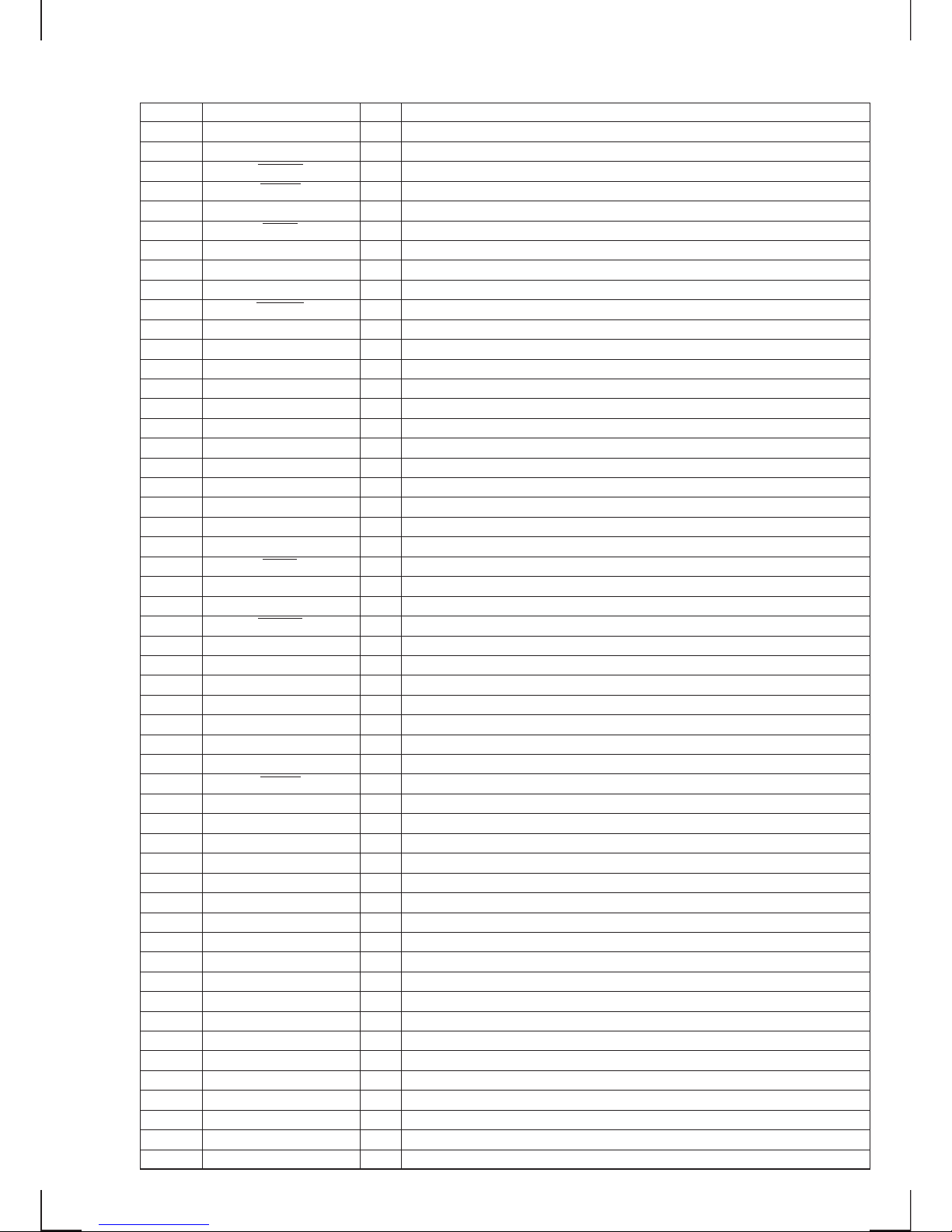
65, 66 TES2, 3 I TEST pin (Fixed at “L”.)
67 VSS2 — Digital GND
68 TEST I TEST pin (Fixed at “L”.)
69 SFDR O Sled drive output
70 SRDR O Sled drive output
71 TFDR O Tracking drive output
72 TRDR O Tracking drive output
73 FFDR O Focus drive output
74 FRDR O Focus drive output
75 VDD2 — Digital power supply
76 COUT O Track number count signal output (Not used.)
77 LOCK O Not used.
78 MDS O Servo control output of spindle motor. (Not used.)
79 MDP O Servo control output of spindle motor.
80 SSTP I Disc most inner track detection signal input
81 FSTO O 2/3 frequency division output of pins 103 and 104.
82 FSTI I Reference clock input for digital servo.
83 XTSL I X’tal select input (“L” : 16.9344 MHz)
84 C4M O 4.2336 MHz output
85 WDCK O D/A interface. Word clock f = 2Fs
86 VDD3 — Digital power supply
87 LRCK O D/A interface. LR clock f = Fs
88 LRCKI I LR clock input to DAC. (48 bit slot) (Not used.)
89 PCMD O D/A interface. Serial data (2’s COMP, MSB first)
90 PCMDI I Audio data input to DAC. (48 bit slot) (Not used.)
91 BCK O D/A interface. Bit clock
92 BCKI I Bit clock input to DAC. (48 bit slot) (Not used.)
93 EMPH O Not used.
94 EMPHI I De-emphasis ON/OFF of DAC. (“H” : ON, “L” : OFF) (Not used.)
95 VSS3 — Digital GND
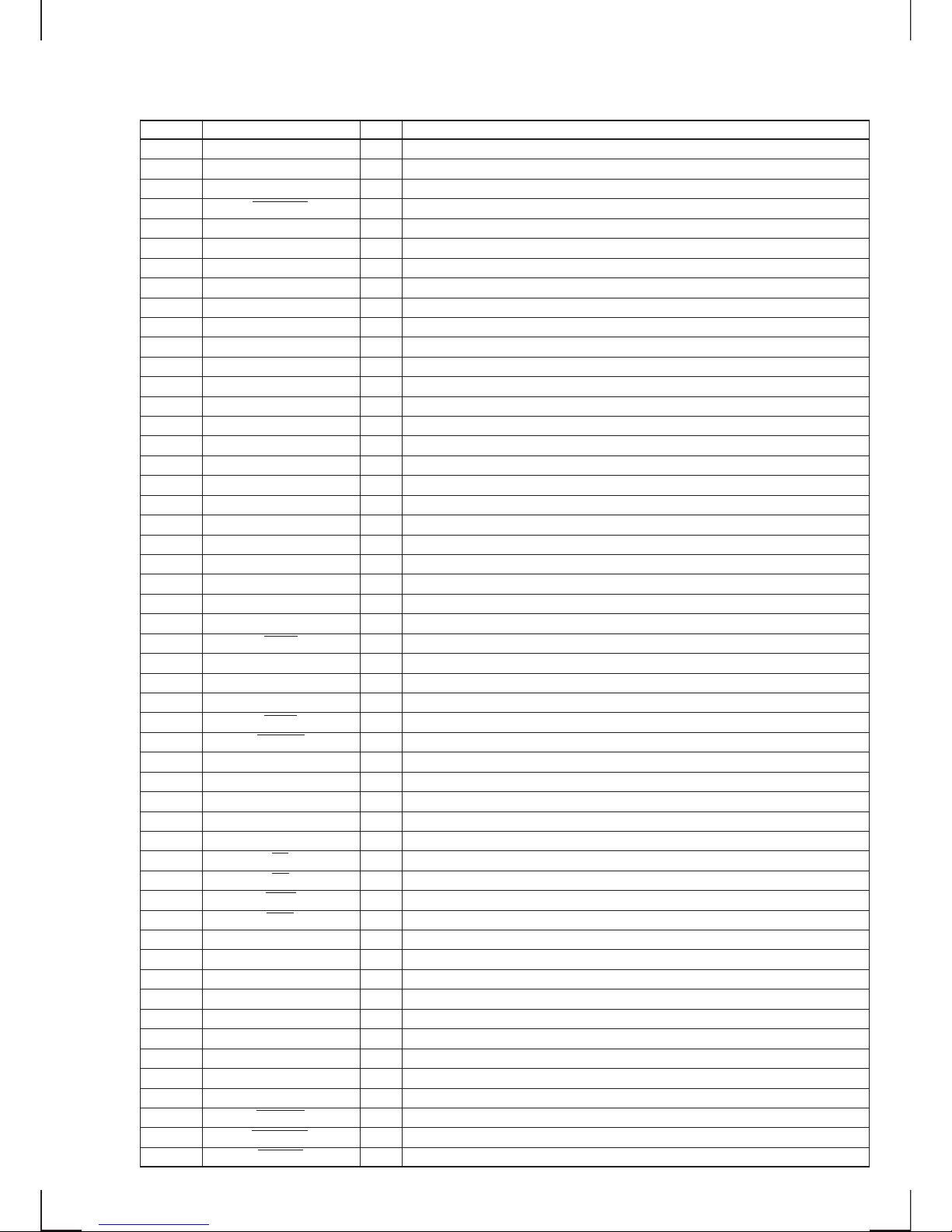
96 AVSS1 — L-ch, Analog GND.
97 AVDD1 — L-ch, Analog power supply.
98 AOUT1 O L-ch, Analog output. (Not used.)
99 AIN1 I L-ch, OP amplifier input. (Not used.)
100 LOUT1 O L-ch, LINE output. (Not used.)
101 AVSS1 — L-ch, Analog GND.
102 XVDD — Analog power supply for master clock.
103 XTAI I X’tal oscillator input of master clock (16.9344 MHz).
104 XTAO O X’tal oscillator output of master clock. (Not used.)
105 XVSS — Analog GND for master clock.
106 AVSS2 — R-ch, Analog GND.