Sony XR-4880 User manual

AEP Model
UK Model
Model Name Using Similar Mechanism XR-C6100R
Tape Transport Mechanism Type MG-25F-136
SPECIFICATIONS
XR-4880
Photo: XR-4880
FM/MW/LW CASSETTE CAR STEREO
MICROFILM
SERVICE MANUAL

– 2 –
TABLE OF CONTENTS
1. GENERAL
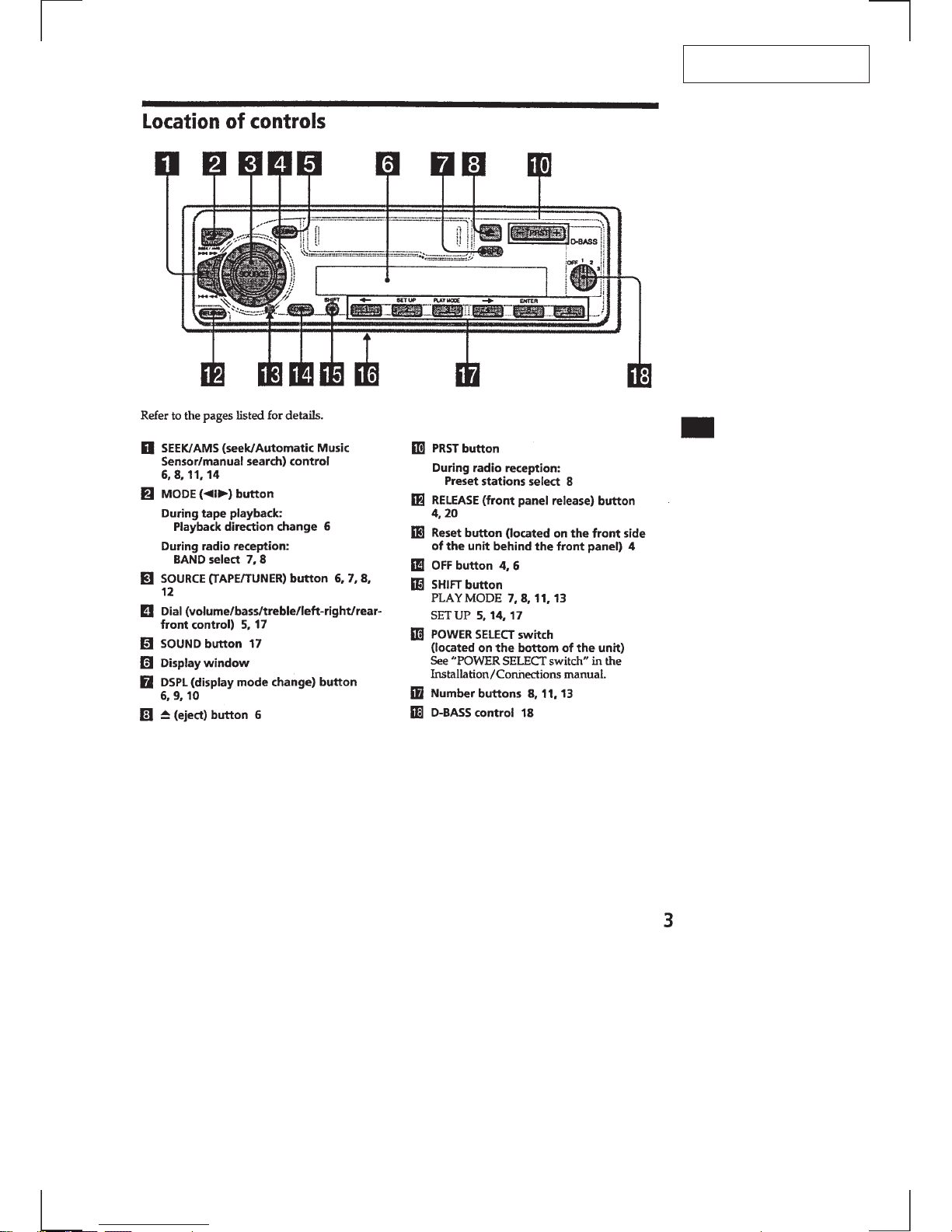
Location of Controls ....................................................... 3
Resetting the Unit ........................................................... 4
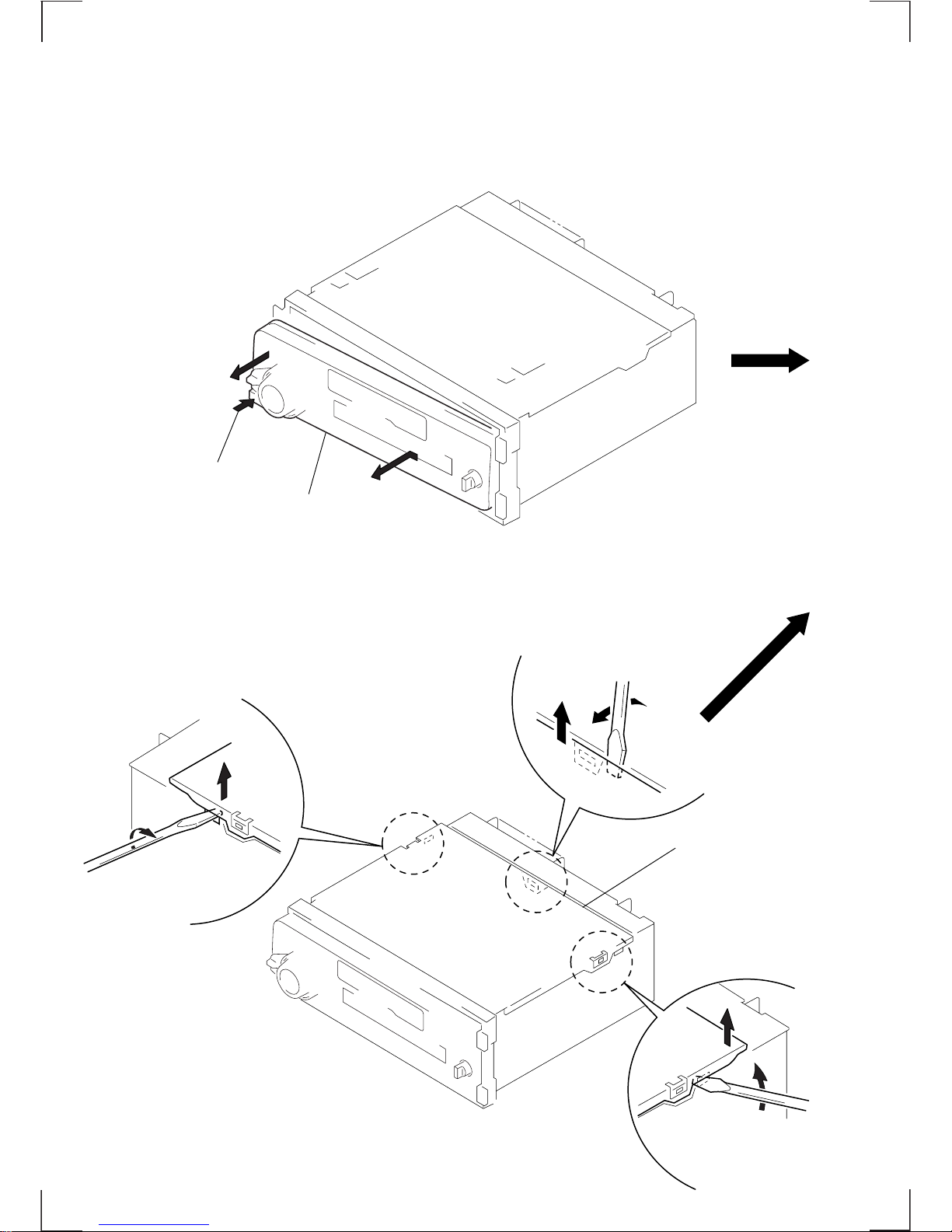
Detaching the Front Panel............................................... 4
Setting the Clock............................................................. 4
Installation....................................................................... 5
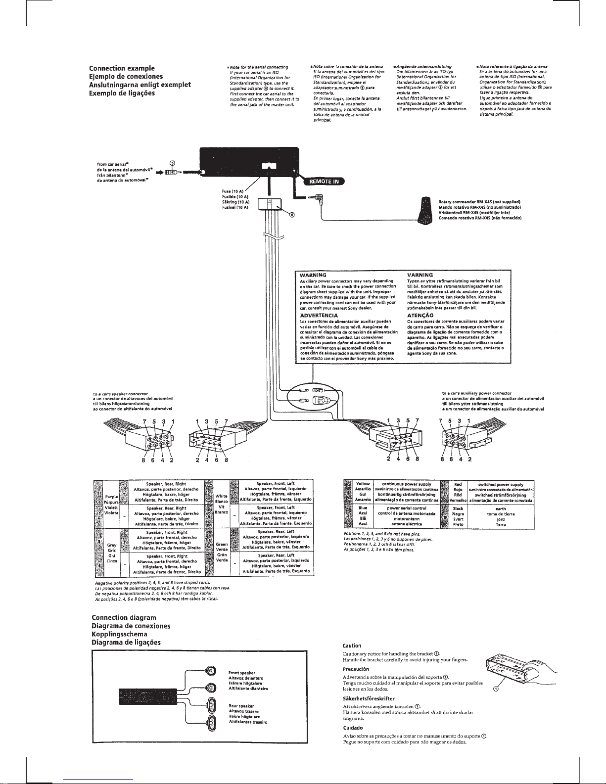
Connections..................................................................... 6
2. DISASSEMBLY ......................................................... 8
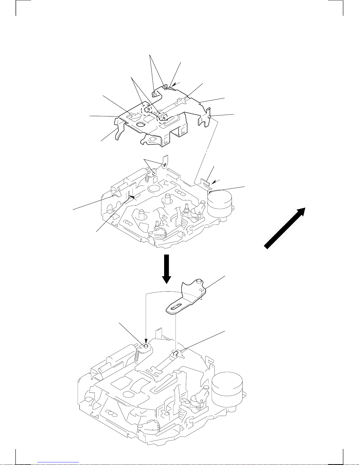
3. ASSEMBLY OF MECHANISM DECK ............ 10
4. MECHANICAL ADJUSTMENTS....................... 13
5. ELECTRICAL ADJUSTMENTS
Test Mode ........................................................................ 13
Tape Deck Section .......................................................... 13
Tuner Section .................................................................. 14
6. DIAGRAMS ................................................................. 17
6-1. Printed Wiring Board –MAIN Section– ........................ 19
6-2. Schematic Diagram –MAIN (1/2) Section–.................. 21
6-3. Schematic Diagram –MAIN (2/2) Section–.................. 23
6-4. Printed Wiring Board –PANEL Section– ...................... 25
6-5. Schematic Diagram –PANEL Section– ......................... 27
6-6. IC Pin Function Description ........................................... 29
7. EXPLODED VIEWS................................................ 31
8. ELECTRICAL PARTS LIST ............................... 34
Flexible Circuit Board Repairing
• Keep the temperature of the soldering iron around 270 ˚C dur-
ing repairing.
• Do not touch the soldering iron on the same conductor of the
circuit board (within 3 times).
• Be careful not to apply force on the conductor when soldering
or unsoldering.
Notes on chip component replacement
• Never reuse a disconnected chip component.
• Notice that the minus side of a tantalum capacitor may be dam-
aged by heat.

– 3 –
SECTION 1
GENERAL This section is extracted from
instruction manual.

– 4 –

– 5 –

– 6 –

– 7 –

– 8 –
FRONT PANEL ASS’Y
COVER ASS’Y
Note: Follow the disassembly procedure in the numerical order given.
SECTION 2
DISASSEMBLY
1
Push the button
(release).
2
Remove the front panel ass’y
to the direction of the arrow
A
.
A
1
1
1
2
2
2
3
Cover ass’y

– 9 –
SUB PANEL, MECHANISM DECK (MG-25F-136)
MAIN BOARD, HEAT SINK
3
Connector
(CN351)
2
Sub panel
1
Three screws
(PTT2.6
×
8)
1
Three screws
(PTT2.6
×
8)
5
Screw
(PTT2.6
×
6)
6
Mechanism deck
(MG-25F-136)
4
Flexible flat cable
(CN301)
3
Two ground point
screws
5
Two screws
(PTT 2.6
×
8)
5
Two screws
(PTT 2.6
×
10)
1
Screw
(PTT2.6
×
8)
5
Screw
(PTT 2.6
×
8)
6
Heat sink
2
Rubber cap (25)
1
Two screws
(PTT2.6
×
8)
4
Main board

– 10 –
SECTION 3
ASSEMBLY OF MECHANISM DECK
Note: Follow the assembly procedure in the numerical order given.
HOUSING
ARM (SUCTION)
1
Install the catch to the hanger.
7
Holder the hanger by bending the claw.
6
Fit projaction on
D
part.
4
Fit claw on
B
part.
5
Fit projection on
C
part.
2
Install the hanger onto
two claws of the housing.
3
Put the housing
under
A
part.
D
part
B
part
A
part
C
part
8
Hold the hanger by
bending the claw.
Hanger
Housing
2
Move the arm (suction) in the arrow
direction and fit on projection.
1
Fit the arm (suction) on the shaft.
Projection

– 11 –
LEVER (LDG-A) / (LDG-B)
GEAR (LDG-FT)
Shaft
A
Shaft
B
Shaft
C
1
Fit the lever (LDG-A) on
shafts
A
–
C
and install it.
3
Type-E stop ring 2.0
Shaft
B
Shaft
A
2
Fit the lever (LDG-B) on
shafts
A
and
B
and
install it.
4
Align hole in the gear (LDG-D)
with hole the lever (LDG-A)
5
Gear (LDG-FT)
6
Polyethylene washer
3
Move the lever (LDG-B)
in the arrow direction.
2
Tensiton spring (LD-1)
2
Tensiton spring (LD-2)
Gear (LDG-FB)
Lever (LDG-A)
Hole
Hole
Gear (LDG-D)
1

– 12 –
GUIDE (C)
MOUNTING POSITION OF CAPSTAN/REEL MOTOR
(M901)
2
Guide (C)
1
Three claws
3
Capstan/reel motor(M901
)
2
Two precision screws
(P 2
×
2)
1
Belt
30
°

– 13 –
SECTION 4
MECHANICAL ADJUSTMENTS SECTION 5
ELECTRICAL ADJUSTMENTS
1. Clean the following parts with a denatured-alcohol-moistened
swab:playback head pinch roller
rubber belt capstan
idlers
2. Demagnetize the playback head with a head demagnetizer.
3. Do not use a magnetized screwdriver for the adjustments.
4. After the adjustments, apply suitable locking compound to the
parts adjusted.
5. The adjustments should be performed with the power supply
voltage unless otherwise noted.
•Torque Measurement
Mode Tension Meter Meter Reading
Forward CQ-403A more than 90 g
(more than 3.18 oz)
Reverse CQ-403R more than 90 g
(more than 3.18 oz)
•TapeTension Measurement
Mode Torque Meter Meter Reading
Forward CQ-102C 30 - 65 g•cm
(0.42 - 0.90 oz•inch)
Forward CQ-102C 0.5 - 4.5g•cm
Back Tension (0.01 - 0.06 oz•inch)
Reverse CQ-102RC 30 - 65 g•cm
(0.42 - 0.90 oz•inch)
Reverse CA-102RC 0.5 - 4.5g•cm
Back Tension (0.01 - 0.06 oz•inch)
FF, REW CQ-201B 60 - 200 g•cm
(0.83 - 2.78 oz•inch)
TEST MODE
This set have the test mode function. In the test mode, FM Auto
Scan/Stop Level and MW Auto Scan/Stop Level adjustments can
be performed easier than it in ordinary procedure.
<Set the Test Mode>
1. Set the “OFF” mode.
2. Push the preset [4] button.
3. Push the preset [5] button.
4. Press the preset [1] button for more than two seconds.
5. Then the display indicates all lights, the test mode is set.
<Release the Test mode>
1. Push the [OFF] button.
See the adjustment location from on page 16 for the
adjustment.
0 dB= 0.775 V
TAPE DECK SECTION
Tape Speed Adjustment
Setting:
Speed checker Frequency counter
–1.5 to +2.5% 2,955 to 3,075Hz
Procedure:
1. Put the set into the FWD PB mode.
2. Adjust adjustment resistor for inside capastan motor so that
the reading on the speed checker or frequency counter becomes
in specification.
Specification: Constant speed
Adjustment Location: See page 16.
+–
test tape
WS-48A
(3 kHz, 0 dB)
speed checker
or
frequency counte
r
4
Ω
set
speaker out terminal

– 14 –
TUNER SECTION 0 dB=1 µV
Cautions during repair
When the tuner unit is defective, replace it by a new one be-
cause its internal block is difficult to repair.
Note:
Adjust the tuner section in the sequence shown below.
1. FM Auto Scan/Stop Level Adjustment.
2. FM Stereo Separation Adjustment.
3. MW Auto Scan/Stop Level Adjustment.
FM Auto Scan/Stop Level Adjustment
Setting:
[SOURCE] button: FM
Procedure:
1. Set to the test mode. (See page 13).
2. Push the [SOURCE] button and set to FM.
Display
3. Adjust with the volume RV2 on TU1 so that the “FM” indica-
tion turns to “FMI” indication on the display window.
But, in case of already indicated “FMI”, turn the RV2 so that
put out light “I” indication and adjustment.
Display
Adjustment Location: See page 16.
FM Stereo Separation Adjustment
Setting:
[SOURCE] button: FM
FM Stereo Level meter Level meter
signal generator connection reading (dB)
output channel
L-CH L-CH A
B
R-CH L-CH Adjust RV4 on TU1
for minimum reading.
R-CH R-CH C
D
L-CH R-CH Adjust RV4 on TU1
for minimum reading.
Procedure:
L-CH Stereo separation: A-B
R-CH Stereo separation: C-D
The separations of both channels should be equal.
Specification: Separation more than 28dB
Adjustment Location: See page 16.
FM RF signal
generator
Carrier frequency : 98.0 MHz
Output level : 22 dB (12.6
µ
V)
Mode : mono
Modulation : 1 kHz, 22.5 kHz deviation (30%)
0.01
µ
F
set
antenna jack (J1)
FM
98.0
SHUF1
FM
98.0
SHUF1
FM RF signal
generator
Carrier frequency : 98.0 MHz
Output level : 70 dB (3.2 mV)
Mode : stereo
Modulation : main: 1 kHz, 33.75 kHz deviation (45%)
sub: 1 kHz, 33.75 kHz deviation (45%)
19 kHz pilot: 7.5 kHz deviation (10%)
0.01
µ
F
set
antenna jack (J1)
+
–
speaker out terminal
level meter
4
Ω

– 15 –
Auto Scan/Stop Level Adjustment
Make this adjustment after "FMAuto Scan/Stop LevelAdjustment".
Setting:
[SOURCE] and [MODE] button: MW
Procedure:
1. Set to the test mode. (See page 13.)
2. Push the [SOURCE] button and set to FM.
3. Push the [MODE] button and set to MW.
Display
4. Adjust with the volume RV1 on TU1 so that the “MW” indi-
cation turns to “MWI” indication on the display window.
But, in case of already indicated “MWI”, turn the RV1 so that
put out light “I” indication and adjustment.
Display
Adjustment Location: See page 16.
AM RF signal
generator
Carrier frequency : 999 kHz
30% amplitude
modulation by
1 kHz signal
Output level : 33 dB
(
44.7
µ
V
)
(50
Ω
)set
AM dummy antenna
30
Ω
15 pF
65 pF
antenna jack (J1)
MW
INTRO 999
SHUF1
INTRO
999
SHUF1

– 16 –
Adjustment Location:
RV1 MW Auto Scan/Stop Level Adjustmen
t
RV2 FM Auto Scan/Stop Level Adjustment
RV4 FM Stereo Separation Adjustment
Tape Speed Adjustment
TU1
—SET UPPER VIEW–

– 17 – – 18 –
IC331 TDA7462D
SE3L
SE3R
MUTE
SDA
SCL
PAUSE
OUT FL
OUT FR
OUT RL
OUT RR
SUBOUT+
SUBOUT–
VDD
GND
CREF
SE1L
SE1R
MD+
MD–
CDL+
CDL–
CDR–
CDR+
PDR
PDGND
PDL
SE2L
SE2R
INPUT
GAIN &
AUTO
ZERO
PAUSE
DETECT
INPUT MULTIPLEXER &
MIXING STAGE
REAR SIDE
SELECTOR
FRONT SIDE
SELECTOR
LOUDNESS
CONTROL
CIRCUIT
INPUT
GAIN
BEEP
LOUDNESS
CONTROL
CIRCUIT
SOFT
MUTE
VOLUME
CONTROL
CIRCUIT
COMPANDER
TREBLE/
BASS
CONTROL
CIRCUIT
SUBWOOFER
OUT
FADER
SUBWOOFER
LP
IIC
BUS
DIGITAL CONTROL CIRCUIT
POWER
SUPPLY
FRONT
FADER
FRONT
FADER
REAR
FADER
REAR
FADER
VOICE BANDPASS
HP LP
SDA
SCL
1
2
3
4
5
6
7
8
9
10
11
12
13
14 15
16
17
18
19
20
21
22
23
24
25
26
27
28
+
–
+
–
+
–
+
–
OVER VOLTAGE
PROTECT
REGULATOR
12 3 45 6 7 8 9 10 1211
NC
MODE2
MODE1
STB
VDD
AMP
VCC
ANT
COM
AM
FM
GND
1 2 3 4 5 6 7 8 9 10 11 12 13 14 15 16 17 18 19 20 21 22 23 24 25
TAB
PW-GND
OUT2–
ST-BY
OUT2+
Vcc1
OUT1–
PW-GND1
OUT1+
SVR
IN1
IN2
S-GND
IN4
IN3
AC-GND
OUT3+
PW-GND3
OUT3–
Vcc2
OUT4+
MUTE
OUT4–
PW-GND4
DIAGNOSTICS OUT
IC661 BA3918-V2
IC751 TDA7385
• IC Block Diagrams – MAIN Board –
IC21 TB2118F (EL)
SECTION 6
DIAGRAMS
IC301 CXA2509AQ-T4
VDD
AMP
AMP
AMP
VDD2
12 3 45 6 7 8 9 10
24 23 22 21 20 19 18 17 16 15
11 12
14 13
XO
OSC
CE
DIN
CK
DOUT
SR
I/O-1
I/O-2
OUT-1
OUT-2
VDD2 IFC
VDD
FM IN
AM IN
D-GND
FM CP OUT
VT
AM CP OUT
VCC
REG
A-GND
XI
SERIAL
INTERFACE
I/O
PORT
OSCILLATOR
ON/OFF
BUFFER
REFERENCE
DIVIDER
PHASE
COMPARATOR
20BIT
IF COUNTER
PRESCALLER
12BIT
PROGRAMMABLE
COUNTER
+
–
REGULATOR
18BIT
18BIT 22BIT
40BIT SHIFT
REGISTER
REF
VCC
SEEK/RECP SEEK/RECP
+
–
SIG
4BIT SWALLOW
COUNTER
OUTPUT
PORT
+
+
+
–
+
–
+–
+
–
+–
12345 6 7 8 9 10
20
19
18
17
16
15
14
13
12
11
2122232627282930
31
32
33
34
37
38
39
40
2425
PBFB1
PBRIN1
PBREF1
PBFIN1
35
36
PBGND
VCT
PBFIN2
PBREF2
PBRIN2
PBFB2
PBEQ1
PBOUT1
VCC
TAPEIN1
AUXIN1
MSLPF
LINEOUT1
NC
NC
G2FB
G1FB
MSTC
DGND
MSOUT
NC
NC
INSW
TAPESW
MSMODE
DRSW
MSSW
NC
NC
LINEOUT2
DIREF
AUXIN2
TAPEIN2
PBEQ2
PBOUT2
GND
F2
120µ/70µ
X1
X1
VCT
+
F1
120µ/70µ24dB
F3
LPF
VCC
DETECT
MS ON/
OFF
FWD/RVS
TAPE EQ
TAPE/AUX
NR BIAS
24dB
MS
MODE
T2
T1
1
2
3
4
56
7
8
9
10
VCC
IN2
S-GND
IN1
NC
NC
OUT2
NC
P-GND
OUT1
CONTROL
CIRCUIT
MOTOR
DRIVE
CIRCUIT
BUFFER
BUFFER
IC351 LB1930M-TLM

– 19 – – 20 –
XR-4880
6-1. PRINTEDWIRING BOARD — MAIN SECTION —
Ref. No. Location
• Semiconductor
Location
Noteon Printed Wiring Board:
•X: parts extracted from the component side.
•¢: internal component.
D1 F-1
D51 E-12
D52 E-11
D351 I-12
D352 G-13
D501 J-5
D551 F-12
D552 F-12
D553 I-9
D554 F-12
D571 D-10
D572 D-10
D581 G-11
D591 F-11
D601 J-13
D610 D-11
D611 D-12
D613 D-11
D614 C-11
D621 E-6
D622 E-7
D623 E-6
D624 E-7
D701 J-3
D702 K-3
D704 K-3
D705 K-5
D706 K-5
D707 K-5
D708 K-5
D709 K-5
D710 J-3
D711 K-5
D712 K-5
D713 K-5
D721 D-8
D722 D-8
D723 D-8
D724 D-9
D731 B-7
D732 D-7
D733 D-7
D734 B-7
D781 D-13
IC21 E-3
IC301 H-4
IC331 D-5
IC351 I-13
IC501 I-7
IC551 J-12
IC611 E-14
IC751 B-7
Q51 E-11
Q52 E-11
Q121 G-4
Q151 G-6
Q171 A-4
Q181 A-3
Q251 G-6
Q271 A-3
Q281 B-3
Q351 H-13
Q352 H-12
Q353 H-12
Q354 H-13
Q551 I-10
Q571 D-9
Q581 G-11
Q591 F-11
Q592 F-10
Q601 J-13
Q602 J-12
Q621 F-7
Q622 F-7
(Page 26)

6-2. SCHEMATIC DIAGRAM — MAIN (1/2) SECTION —
• Refer to page 17 for IC Block Diagrams.
• Refer to page 29 for IC Pin Function Description.
– 21 – – 22 –
XR-4880
Note on Schematic Diagram:
• All capacitors are in µF unless otherwise noted. pF: µµF
50 WV or less are not indicated except for electrolytics
and tantalums.
• All resistors are in Ωand 1/4W or less unless otherwise
specified.
•¢: internal component.
•C: panel designation.
•U: B+ Line.
• Powervoltageisdc14.4Vand fedwith regulated dcpower
supply from ACC and BATT cords.
• Voltage and waveforms are dc with respect to ground
under no-signal conditions.
no mark : FM
< > :TAPE PLAYBACK
∗: Impossible to measure
• Voltages are takenwith aVOM(Input impedance 10MΩ).
Voltage variations may be noted due to normal production
tolerances.
• Waveforms are taken with a oscilloscope.
Voltage variations may be noted due to normal production
tolerances.
• Circled numbers refer to waveforms.
• Signal path.
F: FM
f: AM (MW)
E:TAPE PLAYBACK
•Waveforms
1
2
IC501 !§ XO
IC501 !™ OSC2
2.8Vp-p
18.432MHz
5.0Vp-p
32.768MHz
(Page 23, 24)
A (OFF) →B (ON)
(FL)
FAE342-E01

– 23 – – 24 –
XR-4880
6-3. SCHEMATIC DIAGRAM — MAIN (2/2) SECTION —
• Refer to page 17 for IC Block Diagrams.
• Refer to page 19 for PrintedWiring Board.
Note on Schematic Diagram:
• All capacitors are in µF unless otherwise noted. pF: µµF
50 WV or less are not indicated except for electrolytics
and tantalums.
• All resistors are in Ωand 1/4W or less unless otherwise
specified.
•¢: internal component.
•C: panel designation.
•U: B+ Line.
• Powervoltageis dc 14.4Vand fedwith regulated dcpower
supply from ACC and BATT cords.
• Voltage and waveforms are dc with respect to ground
under no-signal conditions.
no mark : FM
< > :TAPE PLAYBACK
∗: Impossible to measure
• Voltages are takenwith aVOM(Input impedance 10MΩ).
Voltage variations may be noted due to normal production
tolerances.
• Waveforms are taken with a oscilloscope.
Voltage variations may be noted due to normal production
tolerances.
• Circled numbers refer to waveforms.
• Signal path.
F: FM
f: AM (MW)
E:TAPE PLAYBACK
(Page 21, 22)
(Page 27)
Other manuals for XR-4880
3
Table of contents
Other Sony Car Receiver manuals

Sony
Sony XR-C102 User manual

Sony
Sony XS-GTR100L User manual

Sony
Sony CDX-CA650V User manual

Sony
Sony XR-C5300X Product guide

Sony
Sony CDX-S2250EE Product guide

Sony
Sony MEX-1HD - Audio Library System Manual

Sony
Sony CDX-GT740UI User manual

Sony
Sony CDX-GT212 User manual

Sony
Sony MDX-C670 User manual

Sony
Sony CDX-GT200E User manual

Sony
Sony MEX-N5100BE User manual

Sony
Sony XR-C2600 Product guide

Sony
Sony MEX-BT3600U User manual

Sony
Sony MEX-BT3100P User manual

Sony
Sony CDX-F7710S User manual

Sony
Sony CDX-GT550UI (CDX-GT550UI) Product guide

Sony
Sony CDX-C7850 Operating manual

Sony
Sony XAV-3500 Reference guide

Sony
Sony XR-5620 User manual

Sony
Sony CDX-V6800 User manual