manuals.online logo
Brands
  1. Home
  2. •
  3. Brands
  4. •
  5. Sony
  6. •
  7. CD Player
  8. •
  9. Sony CDP-227ESD User manual

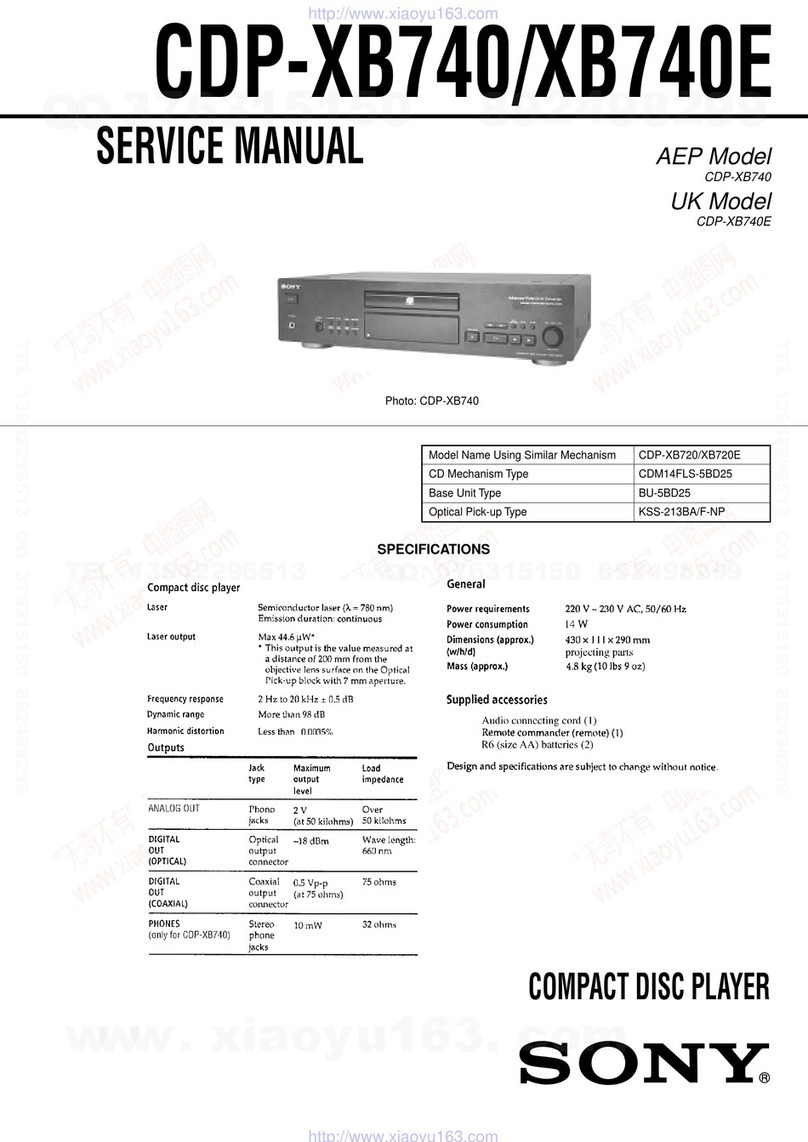
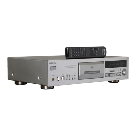
Sony CDP-227ESD User manual

SERVICE
MANUAL
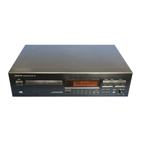
photo:
CDP-507ESD
MICROFILM
LINE
OUT
(FIXED)
(phono
jacks)
Output
level
2
V
(at
50
kilohms)
Load
impedance
over
10
kilohms
LINE
OUT
Output
level
max.
2
V
(at
50
kilohms)
(VARIABLE)
Load
impedance
over
50
kilohms
(phono
jacks)
DIGITAL
OUT
Output
level
0.5
Vp-p
(at
75
ohins)
(COAXIAL)
Load
impedance
75
ohms
|
(phono
jacks)
i
DIGITAL
OUT
Wave
length
(OPTICAL)
660
nm
(optical
output
Output
level
‘connector
-—18
dBm
HEADPHONES
Output
level
max.
(stereo
phone
jack)
|
28
mW
Load
impedance
32
ohms
AEP
UK
US
Canadian
E
Model
Model
CDP-227ESD
Model
Model
Model
CDP-507ESD
Weight
(approx.)
SPECIFICATIONS
Compact
disc
player
General
System
Compact
disc
digital
audio
system
Power
AEP
model
Laser
Semiconductor
laser
(A
=
780
nm)
requirements
(CDP-227ESD)
A
220
V
AC{or
240
V
AC
adjustable
by
Emission
duration
|
Continuous
Sony
personnel),
50/60
Hz
Laser
output
Max.
44.6
uw
UK
model
*
This
output
is
the
value
measured
at
a
(CDP-227ESD)
distance
of
200
mm
from
the
objective
lens
240
V
AC(lor
220
V
AC
adjustable
by
surface
on
the
Optical Pick-up
Block.
Sony
personnel),
50/60
Hz
Frequency
nS
US,
Canadian
model
response
eee
coe
08
(CDP-507ESD)
R ;
120
V
AC,
60Hz
ae
eg
Stee
More
than
106
dB
E
model
:
(CDP-507ESD)
Dynamic
range
More
than
96
dB
110,
120,
220
or
240
V
AC
adjustable,
Harmonic
Less
than
50/60
Hz
distortion
0.0025%
Power
“sith
Wow
and
flutter
Below
measurable
limit
consumption
Channel
More
than
100dB
Dimensions
430
x
110
x
345
mm
separation
(approx.)
(wihid)
(17
x
43/e
x
13/8
inches)
Outputs
including
projecting
parts
and
controls
6.3kg
(13lbs
1502)
Supplied
accessories
Audio
signal
connecting
cord
1
(2
phono
piugs—2
phono
plugs)
Remote
commander
1
Sony
SUM-3
(NS)
batteries
Screw
driver
al
—
Continued
on
page
2—
COMPACT
DISC
PLAYER
SONY.
CDP-227ESD/507ESD
Remote
commander
Optional
accessory
5
Optical
cable
POC-15
Remote
control
Infrared
control
system
Power
3V
DC
with
two
R6
(size
AA)
batteries
requirements
Dimensions
Approx.
62
x
20
x
168.5
mm
(wih/d)
(242
x
Bis
x
64/4
inches)
—
Weight
Approx.
130
g
(5
02)
Note
This
appliance
conforms
with
EEC
Directives
76/889
and
82/499
regarding
interference
suppression.
including
batteries
Features
Variety
of
playing
modes
*
Disc
memo
function
for
writing
a
comment
about
a
disc.
Single
play,
program
play,
shuffle
play
and
repeat
*
Program
bank
function
for
storing
a
programmed
playing
play
as
well
as
normal
continuous
play
of
a
whole
order.
disc.
*
Custom
index
function
for
assigning
your
own
index
point
to
any
desired
position
on
a
disc.
Custom
file
function
Large
and
easy-to-read
window
display
Shows
the
elapsed
playing
time,
the
remaining
time
of
the
selection
being
played,
the
remaining
time
of
the
whole
disc
or
the
remaining
programmed
selection
numbers.
The
display
contains
a
music
calendar
indicating
all
the
numbers
of
the
selections
on
the
disc
Program
play
You
can
play
up
to
20
selections
in
the
desired
order.
Pause
can
be
also
programmed.
You
can
also
confirm
the
total
playing
time
while
choosing
the
selection
to
be
programmed.
Operating
Voltage
Before
connecting
the
unit
to
the
power
source,
check
that
the
operating
voltage
of
your
unit is
the
same
as
the
local
power
line
voltage.
Model
Where
purchased
Operating
voltage
4
ve
AEP
model
Operates
on
220V
AC
(or
240V
AC
adjustable
by
authorized
Sony
!
personnel),
50/60Hz
4
[
UK
model
Operates
on
240V
AC
(or
220V
AC
adjustable
by
authorized
Sony
personnel),
50/60
Hz
Operates
on
120V
AC,
60Hz
I
|
;
Canada
model
i
}
E
modet
Operates
on
either
110, 120,
220
or
240V
AC,
50/60Hz.
The
voltage
selector
is
located
on
the
rear
panel.
If
the
selector
must
be
reset,
disconnect
the
AC
power
cord
and
turn
the
selector
with
a
coin
or
a
similar
object
so
that
the
arrow
mark
of
the
selector
points
to
the
proper
voltage
figure.
ATTENTION
AU
COMPOSANT
AYANT
RAPPORT
A
LA
SECURITE!
SAFETY-RELATED
COMPONENT
WARNING!!
COMPONENTS
IDENTIFIED
BY
MARK
A
OR
DOTTED
LINE
WITH
MARK
/\
ON
THE
SCHEMATIC
DIAGRAMS
AND
IN
THE
PARTS
LIST
ARE
CRITICAL
TO
SAFE
OPERATION.
REPLACE
THESE
COMPONENTS
WITH
SONY
PARTS
WHOSE
PART
NUMBERS
APPEAR
AS
SHOWN
IN
THIS
MANUAL
OR
IN
SUPPLEMENTS
PUB-
LISHED
BY
SONY.
LES
COMPOSANTS
IDENTIFIES
PAR
UNE
MARQUE
/\
SUR
LES
DIAGRAMMES
SCHEMATIQUES
ET
LA
LISTE
DES
PIECES
SONT
CRITIQUES
POUR
LA
SECURITE
DE
FONCTIONNEMENT.
NE
REMPLACER
CES
COM-
POSANTS
QUE
PAR
DES
PIECES
SONY
DONT
LES
NUMEROS
SONT
DONNES
DANS
CE
MANUEL
OU
DANS
LES
SUPPLEMENTS
PUBLIES
PAR
SONY.
TABLE
OF
CONTENTS
Section
Title
Hage.
Specifications
2...
sc.
Sen
bb
oe
bore
See
ees
1
Features:
(coc
eects
Fetes
aL
Se
LOG
eee
ho
2
Operating
Voltage
..........
0...
0.00022
eee
2
Safety
Check-out
....
0...
0.2...
0.0.00
ee
eae
3
Model
Identification
..............2.000008-
3
SECTION
1.
GENERAL
Protection
of
Eyes
from
Laser
Beam
During
SERVICING:
34
58S.
D
tye
ale
Bisinae!
oy
Raat
aeetae
eee
4
Location
and
Function
of
Controls
............
5
Servicing
Note
....
0.0.0.2...
eee
ee
ee
ee
6
SECTION
2.
ADJUSTMENTS
.............--
7
SECTION
3.
DIAGRAMS
3-1.
IC
Block
Diagrams.................-
10
3-2.
Block
Diagram................--055
11
3-3.
Printed
Wiring
Boards
(Display
Section).
.
13
3-4,
Semiconductor
Lead
Layouts
.........
13
3-5.
Schematic
Diagram
(Display
Section)
...
15
3-6.
Waveforms
.........
0.0
cee
eee
ee
eee
19
3-7.
Printed
Wiring
Boards
(Main
Section)
...
20
3-8.
Schematic
Diagram
(Main
Section
1/2)
..
23
3-9.
Schematic
Dlagram
(Main
Section
2/2)
..
26
SECTION
4.
EXPLODED
VIEWS
............
29
SECTION
5.
ELECTRICAL
PARTS
LIST......
34
MODEL
IDENTIFICATION
—
Specification
Label
—
CDP-227ESD
(AEP,
UK
model)
CDP-507ESD
(US,
Canadian,
E
model)
SONY:
won
nGHy
COMPACT
DISC
PLAYER
MMMM
SERIAL
NO.
MADE
IN
JAPAN
CDP-227ESD
AEP,
UK
model:
AC
220—240V
50/60
Hz
CDP-507ESD
US,
Canadian
model:
AC
120V
60Hz
20W
E
model:
AC
110,
120,
220—240V
50/60
Hz
20W
20W
CDP-227ESD/507ESD
CDP-507ESD:
SAFETY
CHECK-OUT
After
correcting
the
original
service
problem,
perform
the
following
safety
check
before
releasing
the
set
to
the
customer:
Check
the
antenna
terminals,
metal
trim,
‘“‘metallized”
knobs,
screws,
and
all
other
exposed
metal
parts
for
AC
leakage.
Check
leakage
as
described
below.
LEAKAGE
TEST
The
AC
leakage
from
any
exposed
metal
part
to
earth
ground
and
from
all
exposed
metal
parts
to
any
exposed
metal
part
having
a
return
to
chassis,
must
not
exceed
0.5
mA
(500
microampers).
Leakage
current
can
be
measured
by
any
one
of
three
methods.
1.
A
commercial
leakage
tester,
such
as
the
Simpson
229
or
RCA
WT-540A.
Follow
the
manufacturers’
instructions
to
use
these
instru-
ments.
2.
A
battery-operated
AC
milliammeter.
The
Data
Precision
245
digital
multimeter
is
suitable
for
this
job.
3.
Measuring
the
voltage
drop
across
a
resistor
by
means
of
a
VOM
or
battery-operated
AC
volt-
meter.
The
“limit’’
indication
is
0.75
V,
so
analog
meters
must
have
an
accurate
low-
voltage
scale.
The
Simpson
250
and
Sanwa
SH-63Trd
are
examples
of
a
passive
VOM
that
is
suitable.
Nearly
all
battery
operated
digital
multimeters
that
have
a
2
V
AC
range
are
suitable.
(See
Fig.
A)
To
Exposed
Metal
Parts
on
Set
|
AC
voltmeter
(0.75
V)
0.15uF
if
S
1,5kQ
=
Earth
Ground
Fig.
A.
Using
an
AC
voltmeter
to
check
AC
leakage.
CDP-227ESD/507ESD
PROTECTION
OF
EYES
FROM
LASER
BEAM
DURING
SERVICING
This
set
employs
a
laser.
Therefore,
be
sure
to
fol-
1.
Laser
Diode
Properties
low
carefully
the
instructions
below
when
servicing.
@
Material:
GaAlAs
@
Wavelength:
780
nm
@
Emission
Duration:
continuous
@
Laser
Output:
max.
44.6
uW*
CAUTION
: ;
*
This
output
is
the
value
measured
at
a
distance
of
Use
of
controls
or
adjustments
or
performance
about
200
mm
from
the
objective
lens
surface
on
of
procedures
other
than
those
specified
herein
the
Optical
Pick-up
Block.
may
result
in
hazardous
radiation
exposure.
2.
During
service,
do
not
take
the
Optical
Pick-up
Block
apart,
and
do
not
adjust
the
APC
circuit.
If
there
is
a
breakdown
inthe
APC
circuit
(includ-
ing
laser
diode),
replace
the
entire
Optiocal
Pick-
up
Block
(including
APC
borad).
eae
anette
te
tie
a
Pn
ee
ee
ee
ee
ee
ee
BESKYTTELSE
AF
O@JNE
MOD
LASERSTRALING
UNDER
SERVICE
I
dette
apparat
anvendes
laserlys.
Derfor
skal
1.
Laser-didoe
data
nedenstaende
instruktioner
noje
felges
under
service.
@
Materiale:
GaAlAs
@
Belgelengde:
780
nm
Folg
iovrigt
instruktionerne
i
servicemanualen.
@
Udstraling:
Kontinuerlig
@
Laseroutput:
Max.
0,4
mW*
*
Malt
i
1,6
mm
afstand
fra
overfladen
af
objektiv-
ADVARSEL!!
linsen
pa
den
optiske
pick-up
enhed.
Under
service
ma
g@jnene
ikke
komme
ner
objektiv-linsen
pa
den
optiske
pick-up
enhed.
|
tilfzelde
af
at
det
er
ngdvendigt
at
kontrollere
udsendelsen
af
laserlys,
skal
det
ske
i
en
afstand
af
mere
end
25cm
fra
den
optiske
pick-up.
@
Klassifikation:
Klasse
Ib.
2.
Adskil
aldrig
den
optiske
pick-up
enhed
under
service,
og
juster
ikke
APC
kredslebet
(Automatic
Power
Control).
Hvis
APC
kredslebet
(incl.
laser-
dioden)
bryder
ned,
skal
hele
den
optiske
pick-up
enhed
(incl.
APC
printkortet)
udskiftes.
LASER
ADVARSEL
MARKNING
Foelgende
mzerkning
findes
indvendig
i
apparatet:
1.
Advarsel
Mzerkning
CAUTION
<
INvisiBLE
LASER
RADIATION
WHEN
OPEN
ANO
INTERLOCKS
DEFEATED,
AVOID
EXPOSURE
TO
BEAM
ADVARSEL
«|
usyNuiG
LASERSTRALING
VED
ABNING
NAR
SIKKEAHEDSAFBAYDERE
ER
UDE
AF
FUNKTION
UNDGA
UDSATTELSE
FOR
STRALING
VAROITUS:
Laite
sisaltaa,
laserdiodin,
joka
lahettaa
(nakymatonta)
silmille
vaarallista
lasersateilya.
CDP-227ESD/507ESD
SECTION
1
GENERAL
LOCATION
AND
FUNCTION
OF
CONTROLS
Front
Panel
CDP-227ESD/CDP-507ESD
CHECK
(program
check)
button
CLEAR
(program
clear)
button
>20
(over
20)
button
FILE
(custom
file)
button
4m
=
INDEX
button
Numeric
buttons
Display
window
INDEX
MODE
button
REPEAT
button
PLAY
MODE
buttons
PROGRAM
button
SHUFFLE
button
A
SPACE/PAUSE
(auto
space/pause)
CONTINUEISINGLE
button
button
DISPLAY
button
LINE
OUT/HEADPHONE
LEVEL
controt
POWER
switch
HEADPHONES
jack
Remote
sensor
ERASE
(memory
erase)
button
TIMER
switch
<4
bP
(manual
search)
buttons
Disc
compartment
kd
BP
(AMS~)
buttons
@
(openiclose)
button
@
(stop)
button
&
(play)
button
Il
(Pause)
button
*
AMS
is
an
abbreviation
of
Automatic
Music
Sensor.
Remote
Commander
PLAY
MODE
buttons
——~—
Numeric
buttons
PGM
(program)
button
SHUFFLE
button
CONTINUE
button
CLEAR
(program
clean
button
SINGLE
button
FILE
(custom
file)
button
(openiclose)
button
C.
INDEX
MODE
(custom
index
mode)
button
ke
PR
AMS
buttons
>20
(over
20)
button
DISPLAY
button
A
<—
B
repeat
button
4m =»
INDEX
buttons
CLEAR/REPEAT
(A
-—
B
repeat
clear!
repeat)
button
<<
BP
(manual
search)
buttons
>
(play)
button
<< pe
SLOW
(low
speed
manual
1
(pause)
button
search)
buttons
@
(stop)
button
LINE
OUT
VOLUME
(line
outfheadphone
volume)
buttons
CDP-227ESD/507ESD
—SERVICING
NOTE
—
MANUAL
OPENING
OF
DISCTABLE
@
How
to
open
the
disctable
manually.
Insert
a
screwdriver(+)
into
the
B
hole
on
the
bottom
plate
as
shown
in
the
figure
and
turn
the
loading
pully
shaft
counter-clockwise,
then
the
disctable
will
push
out
slowly.
Caution
on
closing
the
disctable.
The
disctable
cannot
be
stored
thoroughly
in
the
cabinet,
when
the
optical
block
is
under
a
chucking
state.
To
recover
from
the
chucking
state,
turn
the
driver
through
the
B_
hole
gradually
and
close
the
disctable.
REMOVAL
OF
DISCTABLE
How
to
remove
the
disctable.
y
Pull
out
the
disctable
fully.
Press
the
stoppers
down
with
a
precision
driver
to
release
the
disctable
from
them
and
remove
it.
NOTES
ON
HANDLING
THE
OPTICAL
PICK-
UP
BLOCK
OR
BASE
UNIT
The
laser
diode
in
the
optical
pick-up
block
may
suffer
electrostatic
breakdown
because
of
the
poten-
tial
difference
generated
by
the
charged
electrostatic
load,
etc.
on
clothing
and
the
human
body.
During
repair,
pay
attention
to
electrostatic
break-
down
and
also
use
the
procedure
in
the
printed
matter
which
is
included
in
the
repair
parts.
The
flexible
board
is
easily
damaged
and
should
be
handled
with
care.
—
§—-
SECTION
2
CDP-227ESD/507ESD
ADJUSTMENTS
ELECTRICAL
ADJUSTMENTS
1.
Perform
adjustments
in
the
order
given.
2.
Use
YEDS-18
(8-702-101-01)
disc
unless
otherwise
indicated.
3.
Use
the
oscilloscope
with
more
than
10
MQ
im-
pedance.
Adjustment
Mode
1.
Connect
main
board
test
point
ADJ
and
GND.
This
is
to
prevent
the
disc
table
from
opening
(cre
though
pits
are
not
read,
by
making
micro)
computer
IC301
pin
@)
low.
2.
Turn
POWER
switch
on.
(To
reset
microcomputer.)
After
adjustment,
remove
the
lead
wire
connecting
test
points
ADJ
and
GND.
Adjustment
Location:
main
board
‘CDP-227ESD/507ESD
Focus
Bias
Adjustment
This
adjustment
should
be
made
when
replacing
optical
pick-up.
Procedure:
oscilloscope
(DC
range)
digital
board
oo
TP
(RF)
o———o
TP
(RFG)
1.
Connect
oscilloscope
to
test
points
RF
and
RFG.
.
Put
set
into
adjustment
mode.
.
Turn
POWER
switch
on.
.
Put
disc
(YEDS-18)
in
and
press
»
button.
nA
&
W
NY
.
Adjust
RV104
for
an
optimum
waveform
eye
pat-
tern
or
so
that
the
peak
is
maximum.
Optimum
eye
pattern
means
that
shape
‘‘O”
can
be
clearly
distinguished
at
the
center
of
the
waveform.
Adjustment
Location:
main
board
$$
RF
PLL
Adjustment
Procedure:
frequency
counter
digital
board
fee
=
oy
TP
(PLCK)
ot
ae
TP
(GND)
1.
Connect
main
board
test
point
ASY
and
GND.
2.
Connect
the
frequency
counter
to
main
board
test
points
TP
PLCK
and
TP
GND.
3.
Turn
POWER
switch
ON
(stop
mode).
4.
Adjust
main
board
RV201
so
that
reading
on
frequency
counter
is
4.3218
MHz
+3
kHz.
5.
Reconnect
lead
wires
connected
in
adjustment
mode.
6.
Put
disc
(YEDS-18)
in
and
press
»
PLAY
button.
7.
Confirm
that
reading
on
frequency
counter
is
4.3218
MHz.
Adjustment
Location:
main
board
4
-)
E-F
Balance
Adjustment
This
adjustment
should
be
made
when
replacing
optical
pick-up.
Procedure:
.
Put
set
into
adjustment
mode.
.
Connect
TP(TES)
to
ground.
.
Turn
POWER
switch
on.
.
Put
disc
(YEDS-18)
in
and
press
»
button.
an
wn
.
Adjust
RV101
so
that
the
traverse
waveform
is
symmetrical
above
and
below.
7.
After
adjustment,
cancel
the
adjustment
mode.
VOLT/DIV:
1V
TIME/DIV:
Ims
.
Cnnnect
oscilloscope
to
test
points
TEO
and
GND.
Focus/Tracking
Gain
Adjustment
A
frequency
response
analyzer
is
necessary
in
order
to
perform
this
adjustment
exactly.
However,
this
gain
has
a
margin,
so
even
if
it
is
slightly
off,
there
is
no
problem.
Therefore,
do
not
perform
this
adjustment.
Focus/tracking
gain
determines
the
pick-up
follow-
up
(vertical
and
horizontal)
relative
to
mechanical
noise
and
mechanical
shock
when
the
2-axis
device
operate.
However,
as
these
reciprocate,
the
adjustment
is
at
the
point
where
both
are
satisfied.
@
When
gain
is
raised,
the
noise
when
the
2-axis
device
operates
increases.
@
When
gain
is
lowered,
it
is
more
susceptible
to
mechanical
shock
and
skipping
occurs
more
easily.
@
When
gain
adjustment
is
off,
the
symptoms
below
appear.
e
The
time
until
music
starts
becomes
longer
for
STOP
—>
PPLAY
or
automatic
selection
(K€
PPI
buttons
pressed.
(Normally
takes
about
2
seconds.)
low
or
high
e
Music
does
not
start
and
disc
continues
to
rotate
for
STOP
>PPLAY
or
automatic
selection
(#44
bPt
buttons
pressed.)
®
Disc
table
opens
shortly
after
STOP
>PPLAY.
low
or
high
e
Sound
is
interrupted
dur-
ing
PLAY.
Or
time
count-
er
display
stops
progress-
ing.
e
More
poise
during
2-axis
device
operation.
6.
Connect
oscillo
7.
Adjust
RV304
the
figure
belo
The
following
is
a
simple
adjustment
method.
—
Simple
Adjustment
—
Note:
Since
exact
adjustment
cannot
be
performed,
remem-
ber
the
positions
of
the
controls
before
performing
the
adjustment.
If
the
positions
after
the
simple
adjust-
ment
are
only
a
little
different,
return
the
controls
to
the
original
position.
oscilloscope
(DC
range)
Procedure:
main
board
—_—
TP
TEO
O——7————O
+
!
|
7
®
Incorrect
Exa
|
TP
FEOQ-
-7
lo
1.
Keep
the
set
horizontal.
If
the
set
is
not
horizontal,
this
adjustment
(cannot
be
performed
due
to
the
gravity
saint)
the
2
axis
device.
2.
Put
set
in
adjustment
mode.
3.
Insert
disc
(YEDS-1)
and
press
»
PLAY
button.
4.
Connect
oscilloscope
servo
board
TP
FEO.
high
tracking
ga
5.
Adjustment
RV203
so
that
the
waveform
is
as
(higher
funders
shown
in
the
figure
below.
(focus
gain
adjustment)
VOLT/DIV:
100mV
TIME/DIV:
2mS
—-100mvVv
—ov
@
Incorrent
Examples
(DC
level
changes
more
than
i
Adjustment
Loca
on
adjusted
waveform)
low
focus
gain
VOLT/DIV:
100mVv
TIME/DIV:
2mS
—OoOv
high
focus
gain
VOLT/DIV:
100
TIME/DIV:
2mS
Ge
ee
ce
1D/507ESD
CDP-227ESD/507ESD
Focus/Tracking
Gain
Adjustment
A
frequency
response
analyzer
is
necessary
in
order
to
perform
this
adjustment
exactly.
However,
this
gain
has
a
margin,
so
even
if
it
is
slightly
off,
there
is
no
problem.
Therefore,
do
not
perform
this
adjustment.
Focus/tracking
gain
determines
the
pick-up
follow-
up
(vertical
and
horizontal)
relative
to
mechanical
noise
and
mechanical
shock
when
the
2-axis
device
operate.
However,
as
these
reciprocate,
the
adjustment
is
at
the
point
where
both
are
satisfied.
@
When
gain
is
raised,
the
noise
when
the
2-axis
device
operates
increases.
@
When
gain
is
lowered,
it
is
more
susceptible
to
mechanical
shock
and
skipping
occurs
more
easily.
@
When
gain
adjustment
is
off,
the
symptoms
below
appear.
e
The
time
until
music
starts
becomes
longer
for
STOP
>
DPLAY
or
automatic
selection
(Ké4,
>P>t
buttons
pressed.
(Normally
takes
about
2
seconds.)
low
or
high
@
Music
does
not
start
and
disc
continues
to
rotate
for
STOP>PPLAY
or
automatic
selection
(K¢@
bP
buttons
pressed.)
Jt
e
Disc
table
opens
shortly
after
STOP>DPPLAY.
low
or
high
e
Sound
is
interrupted
dur-
ing
PLAY.
Or
time
count-
er
display
stops
progress-
*
ing.
e
More
poise
during
2-axis
device
operation.
The
following
is
a
simple
adjustment
method.
—
Simple
Adjustment
—
Note:
Since
exact
adjustment
cannot
be
performed,
remem-
ber
the
positions
of
the
controls
before
performing
the
adjustment.
If
the
positions
after
the
simple
adjust-
ment
are
only
a
little
different,
return
the
controls
to
the
original
position.
oscilloscope
Procedure:
ae
a
main
board
&
—_—_—
TP
TEO
cor
ae
1
+
|
TP
FEOQ-
-7
1.
Keep
the
set
horizontal.
If
the
set
is
not
horizontal,
this
adjustment
(cannot
be
performed
due
to
the
gravity
saint)
the
2
axis
device.
.
Put
set
in
adjustment
mode.
.
Insert
disc
(YEDS-1)
and
press
»
PLAY
button.
.
Connect
oscilloscope
servo
board
TP
FEO.
mi
WwW
bh
.
Adjustment
RV203
so
that
the
waveform
is
as
shown
in
the
figure
below.
(focus
gain
adjustment)
TIME/DIV:
2mS
—100mvV
—oOov
@
Incorrent
Examples
(DC
level
changes
more
than
on
adjusted
waveform)
low
focus
gain
—OVv
high
focus
gain
VOLT/DIV:
100
TIME/OIV:
2mS
VOLT/DIV:
100mVv
VOLT/DIV:
100mV
TIME/OIV:
2mS
6.
Connect
oscilloscope
to
main
board
TP
TEO.
7.
Adjust
RV304
so
that
the
waveform
is
as
shown
in
the
figure
below.
(tracking
gain
adjustment)
VOLT/DIV:
TV
TIME/DIV:
2mS
~——OV
@
Incorrect
Examples
(fundamental
wave
appears)
low
tracking
gain
VOLT/DIV:
1V
TIME/DIV:
2mS
—ov
high
tracking
gain
(higher
fundamental
wave
than
for
low
gain)
VOLT/DIV:
1Vv
TIME/OIV:
2mS
—oOov
Adjustment
Location:
main
board
Adjustment
Location:
main
board
[MAIN
BOARD]
CDP-227ESD/507ESD
—mounted
side
—
IRFCI®
STe03
(RF}
e
(ADJ)
lasyYie
@Rv201
RF
PLL
1C204
@(TES)
RV102
TRACKING
GAIN
(GNDJ@
[®RV103
FOCUS
GAIN
(TEO)@
(FEO)
@
@RV104
FOCUS
BiAS
1C204
RV101
EF
BALANCE
CDP-227ESD/507ESD
3-1.
1©C
BLOCK
DIAGRAMS
@
CXA1081S
Yoo
OA16~
OA!
78~
74
-72~62
APTL
APTR
FSw
(1)
ff
MON
(2)
CL¥
SERVO
<
ee
VV
B
.
CORRECTOR
SELECTOR
0
1,
Mos
INSERTER
iy
est
SECTION
3
DIAGRAMS
@
TDA1541
POINTER
inl
@
NJM4556S
DIGITAL
ouT
@
BX1387
VCO
CIRC
TIMING
GENERATOR
4
e
DEMODULATOR
f
fi
cPu
cuKdy
fM
()
|
INTERFACE
ScnCOD
pata
(15)
DE
MODULATOR
a
Seem
cn)
COUNTER
SENS
(8)
SUBCODE
SYNC
GENERATOR
CRCF EXCK
=
SUBQ
SCOR
SOCK
OOTX
080!
~
DBOS
$850
QEX
—GFS
@
TC74HCO2P
Vee
|
4
o
44
YS
83
AS
Yl
Al
al
Y2
a2
B82
GND
HEAD
AMP
RAM
ADDRESS
GENERATOR
Voo
TC74HCOOP
Vee
B4
A4
Y4
83 AS
Y3
LIMITER
Aue
SHIFT
REGISTER
3-2.
BLOCK
DIAGRAM
OPTICAL
PIC-UP
BLOCK
+5V
RF
AMP
/SIGNAL
PROCESSOR
Matec
CDP-227ESD/507ESD
CDP-227E$
¥
A7MH2
OSG
16.9344MHZ
10510
OIGITAL
SIGNAL
PROCESSOR
7CLY
SERVO
/DIGITAL
OUT
!
RV
6)
103
'
RV
102
FE
Ade
9
ae
<TE
(ee
aOEE
LASER
DRIVE
pets
10
Qior
7
fe
*
y
+
5V
2
ap
|
9
Y
TOON
LD.ON
>
©
ae
;
t
3
e
Wy
»
op
28
FOK
+
X
Lt
MUTE
DRIVE
)
|
po
f
DFCT
Fa
852655
%4e
Sas
om
°
(6)
Po
MIRR
re
==
B
%OG
*
J
Veet
oe
eo
+
5V
DFCT
f
4
C
Toe
+<PD
t
<xXRST>
'
DEFECT
ae
;
88
CONTROL
XRST(9)
>
Y
A
DFCT>-mGgorctT
1
=—:1C203
Ww
ul
9
TRK
FCS
ins
FCT
Qt
@9)DFCT
O
TRACKING
FOCUS
(2)-—4)
68%9)
Y
¥
COIL
COIL
3
bt
3
s
=
:
G)ouT2
+2)
ADEFO
be
7
Bs)
ee
y
7
TRACKING
\
/SLED
|
i
SERVO
FOCUS/TRACKING
4
/SLED
SERVO
7
@)ouT)
+IN14(1)
(7)
TAO
54
FSW
@2)
Fsw
>
LD.ON>H{(7)LD.ON
ieooa
mon
1)
Mon
>
FOK
>—@(7)F
OK
|
mop
&9
oP
>—~
—
wr
ck
48)
WFC
H
sLeo
zy
1)
OUTS
(3)
@0)
sLo
h—<
suBa
>-@9
SLED
g
||
—Scor
>#(13)
SCOR
cOIL
©
q
GFS
SWITCH
po!
&9
<
GFS
|
oz06
\V.SOR
,
€2)
ssTOP
PLL.
Switch
()PLLSW
sensor
8
7
a205
|
a
MECHA
CONTROL
a
SENS
@@-t<
SENS
>
<
GFS
(9)
GFs
XRST
@8)
XRST
am
@
-_—_—_-
Data
DATA
h——<
xrsT
(1)XRST
xLt
6
XLT
I~
DATA
@6)
DATA
$251
1
CLK
Gpat—<
CLK
——<
XLT
@4)
LATCH
SPINOLE
——~
CLK
@3)
QUT
M252
DRIVER
LOADING
SWITCH
(M}—@)out2
~N2@)
@5)
sPDLO
DIRCe?
€3)
SPINDLE
NOE
1c
20112/2)
Loapinc"'N1@)
G9)
LIN
od
DRIVER
(M)—@)
ouT
|
LOADING
yc2011/21
MOTOR
+1N1(4)
@9L.
3-3.
PRINTED
NIRING
BOARDS
CDP-227ESD/507ESD
-
CDP-227ESD/507ESD
—
Display
Siction
—
1
2
|
3
4
5
6
|
7
|
8
|
9
10
11
12
Bm
|
4
|
6
SHUFFLE
AUTO
PAUSE
CUSTOM
INDEX
REPEAT
SINGLE
|
AUTO
SPACE
[a]
Pb]
K----—Q2--
BOMOOONBOOOOO-
SR
RHRRARRRBRARERC
RAM
RG
2
Ss
Qbecnaansuuann@hseccenansenennppens
TO
MAIN
BOARD
TO
MAIN
BOARD
TO
MAIN
BOARD
@
©
0
eM
eel
__s
LL
Feee
eo
Ree
een
Rt
ace
Soe
=f
ie
go
aidloact
sie
alee
pIsc
MEMO
TRACK
STEP
INDEX
NEXT
V7
MIN
Ww
sec
a
mM
OC
ooo
—
SESEEnEne
@
Semiconductor
Location
66000000004
CNS
BOT
Location
D-8
E-14
18°
yn
oa
fe}
@
10
n
0:
UF
oO
fe}
a
19
SW
Sof
1
Re
7
OW
5°
a
paipelsele
D-8
“a
12
oma
esl
acele
naga?
o
oO
ix}
oO
wo
o
nD
ow-6
RO22
or
ow-o
Reta
Sa
REG:
[o>]
[«]
[oa
[eee]
[|
[aa
|
|
L>
]
el
"TRE
3-4.
SEMICONDUCTOR
LEAD
LAYOUTS
ee
eer
ear
e
CIRCUIT
BOARDS
LOCATION
NJM5532D-D
LA6520
MSM6408-33SS
NJM4556S
M5F7805
M50740A-424SP
BX1387
28C2021
188132
GPO8PKG23
BA6208
M5F7815
HZS9B2L
10E2N
eee
Bee
52 27
HZS33-2L
LOADING
MOTOR
BOARD
16
1514131211109
we
cathode
nies
aa
See
fd
&
:
pe
1
&
Lo}
1S
2
‘|
view
{
a
12345678
Pe
TER)
ioaesetes
it
i
TOP
VIEW
eo
\
(
Te
tee)
(Top
view)
GNO
out
=)
&
E
oes
a
——]
LC9600P-144
a
ee
a
CXD1144P
M5278L56
CXK5816M-10L
2SC3622A-K
2SB734
TC74HCU04P
Lsciiisee
8
15
(Top
view)
cat
(\
1413121110
9
8
Ec
pine
Output
{
Ground
Vcc
i
hh
x
i)
14
(Top
view)
i
1234567
(Top
we!
CXD10880
DTA114ES
BA1A4M
sioke
(Top
view!
ie
Tt
CXD11250
DTC114ES
BN1A4M
TA7256P
M5F7905
CXP5058H-0600
DTC144ES
iso
ie
i
te
28
IS
M5F7915
:
6523H-3446
|
:
|
Fo}
{
1
14
fa
i
(Top
view)
j
15
|
aT
(Top
view)
pat
vee
Eel
Eo
if
COMMON
IN
OUT
MARKING
SIDE
VIEW
—13—
—14—
$C3622A-K
TA114ES
TC114ES
TC144ES
TO
MAIN
BOARD
x1
28C2021
BA1A4M
BN1A4M
CDP-227ESD/507ESD
Re
Oe
tl
NO
i
2
TO
MAIN
BOARD
OPEN/CLOSE
[1]
18S132
HZS9B2L
H2ZS33-2L
GPO8PKG23
10E2N
@
Semiconductor
Location
Location
D-8
E-14
D-8
[TIMER
BOARD]
PLAY
<—
OFF
a]
e
CIRCUIT
BOARDS
LOCATION
LOADING
MOTOR
BOARD
cathode
anode
enode
DFO2M
POWER
BOARD
TRANSRATION
BOARD
MAIN
BOARD
VOL
BOARD
~
MOTOR
BOARD
JACK
BOARD
1
2
3-5.
SCHEMATIC
DIAGRAM
—
Display
Section
—
iC
DISPLAY
BOARD]
i.
$801
—
S842
:
Push
Switch
a
R617
Reg?
R601
18k
6.
Bk
2.7k
Y
seos
[
sao
|
se03
|
seo
|
sao:
R826
e198
a
Reg2
18k
3.9
ea
Oe
$810
|
S809
|
S808
|
S807
|
S806
fla
bo
R827
RB19
RBI
=
RBO3
18k
«6.8k
3.9K
=
2.7k
b b
3)
9)
)
S815
|
S814
|
S813
|
S812
|
S811
(5)
£4)
£3)
fe)
oy
R628
RB20
R812 R804
18k
=
6.8k 3.9K 2.7k
[se
Se
a
ee,
ets
eg
Ue
pas
|
DISC
MEMO
TRACK
STEP
|
PGM
|
SHUFFLE
AUTO
PAUSE
|
SINGLE
AUTO
SPACE
|
i
$820
|
$819
1
se18
1
sa17
]
sere
a
a
R813 RBOS
6.8k 3.9K
2.
7k
$825
|
S824
|
$623
se22
}
$621
PROGRAM
CONT!
NUE
DD
SHUFFLE
ERASE
RK
R830
R622
RBIS
Rage
18k
6.8K
3.9K
2.
7k
0
6)
GPs
be be
he
$830
|
S829
|
$828
|
S827
|
S826
INDEX
MODE]
[CLEAR
[(>20]
FILE
[CHECK
J
R831
R823)
RBIS
Bad?
18k
6.8k
3.
9k
R832 R824
RBI6
RB08
16K
6.8K 3.9K
2.
7k
R833
10k
AD
R834
10k
:
nme
is
BT
3
‘
e)
Q801
BUFFER
—]5—
1
CDP-227ESD/507ESD
2
3
3-5.
SCHEMATIC
DIAGRAM
—
Display
Section
—
FLUORESCENT
INDICATOR
TUBE
;
(DISPLAY
BOARD]
|
|
|
|
|
|
|
|
|
|
|
|
|
|
|
|
|!
|
|
|
|
|
|
|
|
|
|
|
|
|
|
|
|
|
|
|
|
|
|
|
q
\
!
$801
—
$842
:
Push
Switch
R809
R601
3.9k
=
2.7k
R825
RBI7
18k
6.
8k
R818
RBI0
R802
R826
18k
=6.8k
3.9k 2.7K
bill
&
R827 R819
=RBI1
~=RBO3
18k
6.8K 3.9K
2.
7k
S815
|
S614
|
S613
|
S812
{|
S8i1
(5)
£4]
£3)
fe)
Oy
R828
18k
R820
R812 RBO4
6.8k
3.9K
2.7K
4
5
DISC
MEMO
TRACK
SHUFFLE
AUTO
PAUSE
SINGLE
AUTO
SPACE
FLD801
r
|
L|
R629
R821
RBIS
RBOS
18k
6.
8k
369k
2.
7k
BR
OOOO
()
Sera
a
a
6
CDP-227ESD/507ESD
7
8
FLD80!
INDEX
REPEAT
]
(8)
(c]
Bb)
EE)
)
[oerc>
(2)
(i)
fila
X's)
(9)
()—---—--—--
OSAMA
ADAMI
OOO
MON
OENE)—--
—
BOSSES
OOOSTIOOOOIOOO
aaa
8
Go
a
eer
A
TR
1
aah
SS
se
a
cs
ee
es
ee
a
=i
‘
STEP
INDEX
NEXT
‘
>
BBR
BB
CUSTOM
|
hifzpiah
as
|
|
refi
7frefr9|z0
(Xie)
—
i
N
11
1
4
D
iD
3625
|
se24
|
sa23
|
$822
|
$821
yn
cuna
3
PROGRAM
CONTINUE
DD
yp
cum
2
SHUFFLE
ERASE
D_cuno
|
Ld
Reso
622
Relx
Rens
6
18k
6.8K 3.9K
2.
7k
D
REQ
To]
D
ACK
s|
oa
ut
O
label)
e
|
ie
ore
3830
|
sa29
|
see
|
827
J
$826
Ss
=
eae
INDEX
MODE
($20)
ise
oo
ace
af
ee
pele
nai]
Rei
R623 REIS
REQ7
ae
Ig
18k
6.8K
39k
2.
7k
x
=
2
é|
é
13
eo
U
cae
j
e) ¢) ¢)
o
oO
&
@
1a
se35
|
saa
|
sa33
|
sa3z
|
s831
AC4
ls
(ed
al
Rel
(=)
ar
gc
war
gh
Fe
EY
ince
rn
ee
i
a
ee
ee
Res2
ReZs
ROI6
REDE
}
a
a
eee
Fas
alata
ara
Bl
Peer
sf
a8ot
Seer
seer
h
se4o
|
s839
]
sass
|
se37
|
sea6
3841
|
$842
BUFFER
re
(o>)
(00)
IC801
:
ry
MASTER
CONTROL
!
I
‘Ramm
=
ss
0
comms
coms
©
©
mens
©
©
mom
©
©
mn
©
©
cms
©
©
mms
© ©
comms
+
0
mm
0
mms
ws
cme
©
cm
6
mr
+
m=
mm
=
6
M0
eo
=
©
os
©
a
2
0
MS
©
6
GS
9
8
ms
6
6m
©
mn
0
©
MS
62
SS
8
SS
2
eee
me
+ 6
meme
os
mm
2
0
Sm
2
mee
0
em
On
Oc
MD
0
6
Mn
8
So
2
MOY
so
os
eS
se
—
=
5
1g
0
9
9]
me
iesieeice[e
3600)
13
TIMER
BOARD
J
15
‘cae
ae
4
al’
ar
|
|
|
|
Re
|
|
IC802
aon
REMOTE
SENSOR
$843
_
vey
TIMER
TIMER
L
OF
F-™PLAY
@®
TO
MAIN
BOARD
(2/2)
16
3-6.
WAVEFORMS
CDP-227ESD/507ESD
3-7.
PRINTED
WIRING
BOARDS
—
Main
Sectlon
—
@
Semiconductor
Location
Location
|
Location
1-10
H-6
D-15
1-14
1-14
1-14
G-13
G-l2
H-15
H-16
H-15
H-15
1-12
1-13
1-13
J-12
I-11
1-12
H-10
=
H-8
G-6
F-8
D-7
D-10
E-10
C-7
C-9
@
CIRCUIT
BOARDS
LOCATION
D-2
D-14
D-2
E-14
D-11
C-I1
C-13
E-13
H-13
F-13
1-13
G-15
al
|
C-12
G-15
E-12
1-9
H-6
H-6
H-6
eT
F-7
D-8
C-14
G-14
i
G-14
F-I1
1-12
LOADING
MOTOR
BOARD
POWER
BOARD
TRANSRATION
BOARD
>
:
oye
MAIN
BOARD
in
i
2g
7
VOL
BOARD
7
MOTOR
BOARD
JACK
BOARD
Note:
@
o——-:
parts
extracted
from
the
component
side.
@
@—:
parts
extracted
from
the
conductor
side.
@
@
:
parts
mounted
on
the
conductor
side.
e
:
Jumper
wire
connected
to
the
ground
pattern
on
ae
the
component
side.
:
Pattern
on
the
side
which
is
seen.
CDP-227ESD/507ESD
3-7.
PRINTED
WIRING
BOARDS
—
Main
Sectlon
—
4.6Vp-p
@®
Semiconductor
Location
Location
Location
1-10
D-2
H-6
D-14
D-15
D-2
1-14
E-14
1-14
D-II
1-14
C-11
G-13
C-13
G-12
E-13
H-15 H-13
H-16
F-13
H-15
1-13
H-15 G-15
1-12
F-II
1-13
C-12
1-13
G-15
J-12
E-12
I-11
-
1-12
1-9
4.2Vp-p
-
H-6
H-10
H-6
1-7
H-6
H-8
F-7
G-6
F-7
F-8 D-8
D-7
C-14
D-10 G-14
E-10
F-11
C-7
G-14
C-9
F-11
1-12
5.6Vp-p
@
CIRCUIT
BOARDS
LOCATION
LOADING
MOTOR
BOARD
POWER
BOARD
TRANSRATION
BOARD
MAIN
BOARD
VOL
BOARD
~
MOTOR
BOARD
JACK
BOARD
Note:
@
o——-:
parts
extracted
from
the
component
side.
@
@——:
parts
extracted
from
the
conductor
side.
@
@
:
parts
mounted
on
the
conductor
side.
e
:
Jumper
wire
connected
to
the
ground
pattern
on
na
the
component
side.
:
Pattern
on
the
side
which
is
seen.
=]
CDP-227ES
OPTICAL
PIC-UP
BLOCK
KSS~I5IA
[MOTOR
BOARD]
TO
DISPLAY
BOARD
TO
DISPLAY
BOARD
—
TO
CHASSIS
EARTH
(35887)
[LOADING
SW
BOARD]
$251
LOADING
SWITCH
IN-=—
OUT
-~<o
Xm
TO
DISPLAY
BOARD
CDP-227ESD/507ESD
CDP-227ESD/507ESD
|
4
|
5
|
6
|
7
8
[|
9
|7|
0
|
“”
|
2
TT
8
[|
4
+|
6
Y|
6
17
e@
[|
9
=|
wo
|
2@
22
23
PZ
2
X
[
[POWER
BOARD]
COP-507ESD:
E
MODEL
|
t
[D/O
BOARD)
|
“eQBLECT
Postrion=—
!
|
|
!
|
|
(MAIN
BOARD]
|
!
TO
DISPLAY
BOARD
©
|
‘TO
DISPLAY
BOARD
omc,
!
TOR
BOARD]
!
|
RAY
TRANSMITTER
LINE
OUT
—
DIGITAL
OUT
| |
UNIT
|
|
|
|
|
!
|
I
|
|
|
|
|
|
|
|
401-2
|
[AC
INPUT]
|
a * 4
LINE
OUT
I
|
i
" : i
oi
VARIABLE.
TO
CHASSIS
EARTH
mi
‘ z
See
a
Po
Aap
hs
. : “
:
|
|
[Raeeeay.
ION
|
BOARD
!
=
=
ON
OFF
|
a
ee
ee
J
SE
ST
SPA
OTGRROAL
The
SCOR:
S07ESD.
fp
eee
ee
ee
SS
Sepp
oozpepe
al
7
{POWER
BOARD)
Geers
oper.
>
fh
[POWER
BOARD)
AEP.UK
MODEL
!
\
I
|
eect
A
|
|
7
1
|
|
|
[ol
I
|
|
|
|!
|
I
|
|
|
|
Ly
|
er
|
kee
of
|
I
al
|
La
lo
|
|
|
|
| |
|
|
|
|
|
|
|
ly
WHT
|
POWERTRANSFORMER
|
|
POWER
TRANSFORMER
|
|
|
|
ly
|
|
|
|
|
|
i
|
|
|
|
$25!
|
|
|
LOADING
SWITCH
|
iN<—
OUT
!
\ |
|
Se
J5
i
a
ne
ea
ce
prec
ir
ae
emesis
hos
ly
eed
i
eb
pene
|
ame
em
me
me
me
cme
me
a
ae
ee
ae
—21-
—29—
1
3-8.
SCHEMATIC
DIAGRAM
2 3
4
—
Main
Section
(1/2)
—
@
Signal!
path
ewe
:cd
Zz:
digital
out
:
|
'
l
:
|
'
|
:
|
:
|
'
|
‘
|
'
|
'
\
:
|
:
I
‘
|
'
1
'
|
'
!
:
!
:
@
See
page
28
for
note.
10
11
{MAIN
BOARD
(172)
]
SP
|INDLE/LOADING
DRIVE
IN.
SW
L.
MOTOR
1C201
TA7256P
R205
120k
R206
150K
IC203
DEFECT
CONTROL
R225
Tk
eld
He
3
(3)
SENS
@)
CLK
wt
LATCH
@)
“oso
DIRCT
_O
zoe
w
(=)
vss
t=)
SUBG
L{=)
GFS
Pye)
WFCK
(
AEP,UKE
MODEL
)
C208
0.015
R217,
680!
680k
fe)
G
SW
ane
]
laesaalilca)|
BOARD
|
a
peas
AS:
be)
poo
Wye,
||
ed
|
LOADINGW!
vcr
(LK
|
|
MOTOR
M251
obese
a)
0;
ual
&
BOARD
Aj
®
7
-tHUL
om
aaa
7B
Ae
@-
oe
23—(o}
M252
pa
|
Ly
|
tj
|
Lj
i
tj
ij
|
~~
L)
scenes
|
fs
ley
bi
i
(1
8
[2
wHi><|
rr)
|
eves
|
©
|
a
3)
rs
|
rant
|
|
|
|
OPTICAL
PICK-UP;
BLOCK
KSS-151A
|
eae
=
|
iA\
SLED
Q)
7,
4
i
ae
9
fy
fa
OE
ee
came”
pp.
wTr
Leg)
t2
a
(<4)
%
@
R218
100k
C209
0.047
4+
1€202
LA6S20
cp.
101
D101
reD
PROTECTOR
gio1
258734
95
£106
22/25,
€107
0.
0033
Q101
4
2
LASER
DRIVEGND
RF
1C101
CXA1081S
RF
AMP
<FOK>-
<LD.
ON
—--<XRST
>
<DIRC>
<CLK>—
<XLT>
<DATA>—
<SENS>
Te!
R222
130k
<TAO>
<FEQ>——
<SPDLO>
<DFCT>
<FOK>
<LD.
ON>
C118
2200p
CI13
22/25
o>
Cité
0.
7S|1GNAL
PROCESSOR
<MON>
~<MDP-
RF
PLL
FREQUENCY
C227
22/25
<ASY.
TO
MAIN
BOARD
(2/2)
|
FOCUS/TRACK
7SLED
SERVO
FOCUS
GAIN
FOCUS
BIAS
ING
P
Q206
GFS
SWITC
12
13
14 15
MECHA
CONTROL
TO
MAIN
BOARD
(2/2)
TO
DISPLAY
BOARD
ooo
oreiey|
FILE
DATA
CONTROL
Sy
Bl
a
a
a
a
a
a
a
eT)
(|)
ee
ee
ee
Q301
MUTE
DRIVE
|_|
=
<MON>
<MDP
>
—+-
FSW:
>
ens
=o
ASY>
LOCK
<VCO>
PDO:
t+—O
MDP
pe ee
et
|
ene
ia
ee
ae
Fy
-
XLT
°
ieee
ae
a
gs
‘
|
EFM
-
MIRR
s
3
a205
—<-
=
;
T]
83
BALEM
tt
rst
3
,
(EB)
g
.|=
at
2a
re:
|
8
$
+
1
AAAAAKQARLESD
4.5
0
3
BS
ag
EG848748538
GFSO
0
=
2
ey
yey
oy
2G
(5)
aA
a
2
|
le
y=
uy
=|
oO
ia
|
|
|
aa
J
eae
(
js -2
||
2.3
1352
LC9600R-145
1€302
CxXD1125
a
mone
zz
aan
ae
PLL
SWIT
3
CH
:
FILE
MEMO
A
Ny
1206
.;
§
FS
SWITCH
1C303
IC302
|
{
|
RAM
DIGITAL
SIGNAL
PROCESSOR?
£&
2
£§
x.
/CLV
SERVO/DIGITAL
OUT
=
#
€
6
28@
B\2
es
Pale
ee
1
TO
MAIN
BOARD
(2/2)
a
as
a
aes
matt
enc
eS
a
sehen
Taam
ee
een
ems
cate
Semen
|
_
©
@
|
TO
MAIN
BOARD
(2/2)
|
Ree
ee
Pree
I
—24—
—25—
1
3-9.
SCHEMATIC
DIAGRAM
—
Main
Section
(2/2)
—
2
3
4
5
6
7
8
9
10
11
1
[MAIN
BOARD
(2/2))
rie
+5V
REG
**\
D902
1SS8132T-7:
TO
MAIN
BOARD
(1/2)
[ee
ee
Te
BSV
be
COM
Vi
Texsfeya
1/2
4
ty?
G
INVERTER
VE
Care
7
28
%
Q940
=
|
-30VREG
IC920
A!
whi
Ed
UK
AEP.E
se
MODEL
53
SETS
IC921
ficg22
DIGITAL
FILTER
=0¥
REG
esos
BICSee
D/A
CONVERTER
$9805
Tocky
IC930
-15V
REG
LRCK
|
p>
;
}
|
DATA
[Toa
ik
obs
cvs
|
|
,
.
i
co,
eee
(7MHz
|
4/6)
XIN
S
DATAR
33
oor
Pe
gE
e8
fi
IP
Bo
a
R401
TO
MAIN
BOARD
(1/2)
“owt
Fs
.
ics21
Q400,500
380
|
ae
erro
DAIS41-
ewiee
D.MUTE
(5)
BCK
SWITC
C40"
|
4045
MUTE
LRCK
D>
>
L—@)
TEST
|
APT/WS
v
ae
(2)
BFS/EFM
ADPT
1C510
MC74HCU04
&
Nn
M5F7805
oe
Pr
a
DECOU
=s
DECOU
D
DECOU
1C931
MBF7905
I7MHz
OSC
RESET
ae
DE.EMP
Os
hon
iene
se
TO
MAIN
BOARD
(1/72)
4,
8
3
(T¥
“tal
By
uh)
9
Lorexsie)
wi
eet
con
BATASM-TP
%®
_-RY500
aa
INVERTER
otcyer2§
2/2
ete
ES
MUTING
GATE
gsgs
RAY
TRANSMITTER
UNIT
pe
as
ar
Se
Set
ee
Es
IN
ea
as
Ss
5a
|
r
te
fe
oe
fod
Torx
j
KVOL
BOF
cD:
wee
ine
j
1C391
BA6Z0
7
a
j
3
i
|
8
[D/O
BOARD]
=
-
ere:
Sa
ae
gt
aa
=]
1¢380
.
|
DIGITAL
OUT
|
C7
4HCOON
|
;
8380
ON/OFF
sw
F
\
i
I
ON
58
|
J380
@)
+
:
R362
WY
!
|
of
4
se
J380
TO
MAIN
BOARD
(I/2)
:
Yan
DOTX
_
ea
‘
is.
See
eh
+]
pond
c=
|
io"
@
PPT
tp
me
Ts
wo
es
tL
big
!|
our
EEL
eu
nD
earache
oe
[le
ve.
(er
yd
ae
| I
MOTOR
DRI\
TO
MAIN
BOARD
11/2)
woz
fot
eux
aaa
1380
ca
|
|
pe
cne0
|
z=
a
|
|
|
|
&
|
|
;
|
|
:
1
JOUTPUT
|
|
|
|
[SELECTOR
|
|
Se
es
as
hs
hn
a
a
I
biota
ieee
conve
eta)
j
a
a
OUT
[ens
eet
7
LINE
OUT
12
13
14
15
16
17
18 19
UKAEPE
//
MODEL
H
““~"“TpoweR].
«|
=
CDP-607ESD:
US,Canadian
MODEL
LOH
AC
85
7
O
ORG
(Pon
tee
a
Et
ee
Seagate
pee
ge
;
(POWER
BOARD)
i
eee
eS
Yada
im
+
UK
MODEL
:
CDP-227ESD:
}
1
T901
AEP,UK
MODEL
j
i!
a
:
at
J 2 .
1
it
!
4
1
"1
1
tl
4
a
FI
©
r
!
!
!
|
'
'
i
‘
I
t
i}
'
'
1
I |
|
|
!
| !
!
!
|
|
'
t
' ' '
1
' '
|
'
L
ons
fon
Gast
feos
i
Ye
os
iS
a
a
a
dc
a
nS
Ss
Pee
--------4
A
D920—9323
RECT
eoew
wen
ny
c920
LO
UK
AEP,E
MODEL
R403
4.7k
LINE
AMP
oO]
5
+15V
!
CNP902
é
O
n
Q
°
=
CNJ391
J40i-1
LINE
OUT
FIXED
CNJ393
J401-2
LINE
OUT
VARIABLE
NJM5532D
272
Ketstere)
“
LINE
AMP”
Q520,522
“
INVERTER,”
CNJ391
a
aa
set
as
ea
ee
ee
ess
sc
es
ne
a
le
ves
is
sf
ee
ve
7
BOAR
DI
wsuassegi
2
yAsg
US
sae)
i
1391
BA6208
7
RR
ruse”
HEADE
HONE
AMP
4,
pwacrey
3R
awa
ipers
8
BLK
ow
2
mol
Be
CNJ393,
|
I
LINE
OUT
PHONE
LEVEL
Pr
eet
x
[MOTOR
BOARD]
s
CNu391
Pele
L
8
ii
Hipa
Pee)
ey
sala
|
|
a
OR
DRIVE
be
be
ee
iT
N'
E>
RED
rh
|
E>
3
fetes
Fe
de
ae
pe
J390
sr]
en)
ee
ae
U
Ly
H
Gao
1
HEADPHONES
|
om
su
lise
|i]
TT
!
i
cxsms
GSS
sie
20
21
22
Note:
All
capacitors
are
in
uF
unless
otherwise
noted.
pF:
uwuF
50WV
or
less
are
not
indicated
except
for
electrolytics
and
tantalums.
All
resistors
are
in
Q
and
1/,W
or
less
unless
otherwise
specified.
4:
internal
component.
fu}
:
fusible
resistor.
ome
©
B+
lin.
aaa
;
B-
lin.
[—]
:
adjustment
for
repair.
Voltage
and
waveforms
are
dc
with
respect
to
ground
under
no-signal
conditions.
no
mark:
STOP
Voltages
are
taken
with
a
VOM
(50kQ/V).
Voltage
variations
may
be
noted
due
to
normal
produc-
tion
tolerances.
Waveforms
are
taken
to
grow
by
using
ocilloscope.
Voltage
variations
may
be
noted
due
to
normal
produc-
tion
tolerances.
Circled
numbers
refer
to
waveforms.
(See
page
18.)
Signal
path.
e&
:CD
e>
:
digital
out
Switches:
Ref.
No.
Switch
Position
$251
LOADING
SWITCH
OUT
DIGITAL
OUT
OFF
OFF
OFF
OFF
OFF
OFF
OFF
$380
OUTPUT
SELECTOR
$801
$802
$803
$804
$805
$806
$807
$808
OFF
$809
OFF
$810
OFF
$811
OFF
$812
OFF
$813
OFF
$814
OFF
$815
OFF
$816
OFF
$817
OFF
$818
OFF
$819
OFF
$820
OFF
$821
OFF
$822
ERASE
OFF
$823
CONTINUE/SINGLE
OFF
$824
SHUFFLE
OFF
$825
PROGRAM
OFF
$826
>20
OFF
$827
CHECK
OFF
$828
CLEAR
OFF
$829
FILE
OFF
$830
INDEX
MODE
OFF
$831
INDEX
>
OFF
$832
.
OFF
$833
AMS
€4
OFF
$834
AMS
ppl
OFF
$835
«
OFF
$836
DISPLAY
OFF
$837
OFF
$838
A-PAUSE
OFF
$839
REPEAT
OFF
$840
INDEX
<
OFF
$841
>
OFF
$842
"
OFF
$843
TIMER
OFF
$990
POWER
OFF
vsg901
VOLTAGE
SELECTOR
-
(E
model)
OMAN
OOARWDHDN
=
Note:
The
components
identified
by
mark
A
or
dotted
line
with
mark
A
are
critical
for
safety.
Replace
only
with
part
number
specified.
CDP-227ESD/507ESD
CDP-227ESD/507ESD
SECTION
4
EXPLODED
VIEWS
2.
CHASSIS
NOTE:
@
The
mechanical
parts
with
no
reference
@
Due
to
standardization,
parts
with
part
The
components
identified
by
number
in
the
exploded
views
are
not
number
suffix
-XX
and
-X
may
be
dif-
mark
A
or
dotted
line
with
mark
supplied.
ferent
from
the
parts
specified
in
the
are
critical
for
safety.
components
used
on
the
set.
eplace
only
with
part
number
specified.
@
The
construction
parts
of
an
assembled
part
are
indicated
with
a
collation
num-
@
Color
Indication
of
Appearance
Parts
ber
in
the
remark
column.
See
KNOB,
BALANCE
(WHITE
Les
composants
identifiés
par
une
@
Items
marked
"*"
are
not
stocked
since
t
as
a
t
}
marque
sont
critiques
pour
ja
they
are
seldom
required
for
routine
securite,
service.
Some
delay
should
be
antici-
Cabinet's
Color
Parts’
Color
Ne
les
remplacer
que
par
une
pated
when
ordering
these
items.
piéce
portant
le
numéro
spécifé.
1.
GENERAL
§2—=1-se|s2-
51
Note:
Note:
The
components
identi-
|
Les
composants
identifiés
par
fied
by
mark
or
dot-
|
une
marque
sont
critiques
ted
line
with
mark
pour
la
sécurité.
are
critical
for
safety.
Ne
les
remplacer
que
par
une
Replace
only
with
part
|
piéce
portant
le
numéro
spéci-
number
specified.
fié.
Ref.No
Part
No.
Description
Ref.No
Part
No.
Description
51
7-685-647-79
SCREW
+BVTP
3X10
TYPE2
N-S
67
4-922-915-01
FOOT
(FELT)
52
X-4922-508-1
FOOT
ASSY
68
*
4-886-555-00
HEAT
SINK
53
*
4-922-928-01
CHASSIS
69
7-682-547-09
(E)....SCREW
+BVTT
3X6
(S)
54
7-685-661-79
SCREW
+BVTP
4X12
TYPE2
N-S
901
»*A-4651-177-A
(E,UK)....MOUNTED
PCB,
MAIN
55
4-923-520-01
KNOB,
POWER
901
»*A-4651-198-A
(Canadian,
US,
AEP)....MOUNTED
PCB,
MAIN
Ref.No
Part
No.
Description
Ref.No
Part
No.
Description
56
*
4-922-530-01
LEVER,
POWER
SWITCH
903
1-464-878-11
TRANSMITTER
UNIT,
RAY
57
*
4-885-838-01
(AEP,
UK,
£)....LABEL,
CLASS1
904
=
*
1-§35-122-00
TERMINAL
2
A-4675-247-A
(AEP,
UK,
E)....PANEL
ASSY,
LOADING
8
4-886-821-01
SCREW,
M3
CASE
58
*
3-703-244-00
BUSHING
(2104),
CORD
905
»*1-535-139-00
BASE
POST
19MM
(10MM
PITCH)
2P
2
A-4675-248-A
(US,
Canadian)....PANEL
ASSY,
LOADING
9
4-922-528-01
LID,
BATTERY
CASE,
COMMANDER
59
4-909-982-01
SCREW,
TAPPING
906
=
*1-535-688-11
TERMINAL
3
7-685-647-79
SCREW,
TAPPING
10
*
4-922-927-51
PLATE,
BOTTOM
60
7-621-775-10
SCREW
+B
2.6X4
914
*1-626-469-11
PC
BOARD,
POWER
4
*
4-917-634-01
DAMPER
(C)
11
1-463-909-11
COMMANDER,
REMOTE
(RM-D650)
61
*
4-922-505-12
(US)....PANEL,
BACK
915
+*1-626-470-11
PC
BOARD,
D/O
5
*
4-922-422-01
CUSHION
(C)
12
4-923-533-01
BOLT
(M2.6X3),
HEXAGON
SOKET
61
*
4-922-505-22
(Canadian)....PANEL,
BACK
921
A\.1-555-795-00
(AEP)....CORD,
POWER
6
7-685-646-79
SCREW,
TAPPING
13
7-685-871-01
SCREW
+BVTT
3X6
(S)
61
*
4-922-505-32
(UK)....PANEL,
BACK
921
A\.1-556-035-00
(UK)....CORD,
POWER
7
4-922-594-01
CASE
14
X-4922-521-2
PANEL
ASSY,
FRONT
61
*4-922-505-42
(AEP)....PANEL,
BACK
921
A\.1-557-577-11
(US,
Canadian)....CORD,
POWER
61
*
4-922-505-51
(E)....PANEL,
BACK
921
A\,1-558-181-11
(E)....CORD,
POWER
62
*
4-913-152-01
ESCUTCHEON,
D/O
T901
A\.1-449-285-11
(US,
Canadian)....
TRANSFORMER,
POWER
63
*
4-908-502-01
HEAT
SINK
T901
A\.1-449-286-11
(AEP,
UK)....
TRANSFORMER,
POWER
64
*
3-309-144-01
HEAT
SINK
T901
A\.1-449-287-11
(E)....
TRANSFORMER,
POWER
65
7-682-147-15
SCREW,
TR
VS901A\.1-526-576-51
(E)....SELECTOR,
POWER
VOLTAGE
66
*
4-922-525-01
HEAT
SINK
—29—
—30—

This manual suits for next models

1

Other Sony CD Player manuals

Sony CDC-R504MP User manual

Sony

Sony CDC-R504MP User manual

Sony DVP-C600D - 5 Disc Cd/dvd Player User manual

Sony

Sony DVP-C600D - 5 Disc Cd/dvd Player User manual

Sony CDX-GT572 User manual

Sony

Sony CDX-GT572 User manual

Sony CFD-ZW150 User manual

Sony

Sony CFD-ZW150 User manual

Sony MDP-600 User manual

Sony

Sony MDP-600 User manual

Sony D-E561 Primary User manual

Sony

Sony D-E561 Primary User manual

Sony D-NF400PS - Portable Cd Player User manual

Sony

Sony D-NF400PS - Portable Cd Player User manual

Sony MZ-S1 SonicStage v1.5 User manual

Sony

Sony MZ-S1 SonicStage v1.5 User manual

Sony CFD-G35 - Cd Radio Cassette-corder User manual

Sony

Sony CFD-G35 - Cd Radio Cassette-corder User manual

Sony CDP-CE375 User manual

Sony

Sony CDP-CE375 User manual

Sony Walkman D-FJ211 User manual

Sony

Sony Walkman D-FJ211 User manual

Sony CDX-GT414U User manual

Sony

Sony CDX-GT414U User manual

Sony CDX-G3205UV User manual

Sony

Sony CDX-G3205UV User manual

Sony CFD-S47 - Cd Radio Cassette-corder User manual

Sony

Sony CFD-S47 - Cd Radio Cassette-corder User manual

Sony CDP-D500 User manual

Sony

Sony CDP-D500 User manual

Sony D-303 User manual

Sony

Sony D-303 User manual

Sony D-NF611 - Portable Cd Player User manual

Sony

Sony D-NF611 - Portable Cd Player User manual

Sony CDP-CX450 - Compact Disc Player User manual

Sony

Sony CDP-CX450 - Compact Disc Player User manual

Sony CFD-V35 - Cd Radio Cassette-corder User manual

Sony

Sony CFD-V35 - Cd Radio Cassette-corder User manual

Sony DNE330S User manual

Sony

Sony DNE330S User manual

Sony CDP-M555ES - Es 400 Disc Cd Changer User manual

Sony

Sony CDP-M555ES - Es 400 Disc Cd Changer User manual

Sony XP-EV500 User manual

Sony

Sony XP-EV500 User manual

Sony S350 - CFD Boombox User manual

Sony

Sony S350 - CFD Boombox User manual

Sony Walkman MZ-E3 User manual

Sony

Sony Walkman MZ-E3 User manual

Popular CD Player manuals by other brands

Coby COBY MP-CD551 Specifications

Coby

Coby COBY MP-CD551 Specifications

Casio ZD-3 Service manual

Casio

Casio ZD-3 Service manual

Pioneer CDJ-400 - Cd/Media Player Frequently asked questions

Pioneer

Pioneer CDJ-400 - Cd/Media Player Frequently asked questions

Philips Jogproof AX5114 Specifications

Philips

Philips Jogproof AX5114 Specifications

DAPAudio D1183 instructions

DAPAudio

DAPAudio D1183 instructions

CMS EZ BELLS operating manual

CMS

CMS EZ BELLS operating manual

Kenwood DPC-191 instruction manual

Kenwood

Kenwood DPC-191 instruction manual

DVS VE-200 user manual

DVS

DVS VE-200 user manual

Blaupunkt CDC A03 Operating and installation instructions

Blaupunkt

Blaupunkt CDC A03 Operating and installation instructions

Philips CDI 615 Technical documentation

Philips

Philips CDI 615 Technical documentation

Philips AZ1826 Quick use guide

Philips

Philips AZ1826 Quick use guide

Jensen CD-476 instruction manual

Jensen

Jensen CD-476 instruction manual

Philips AX2001 Specifications

Philips

Philips AX2001 Specifications

Pioneer PD-95 operating instructions

Pioneer

Pioneer PD-95 operating instructions

Pioneer CD-8400 Service manual

Pioneer

Pioneer CD-8400 Service manual

JVC XL-MC2000BK instructions

JVC

JVC XL-MC2000BK instructions

Philips AZ6840/05 user manual

Philips

Philips AZ6840/05 user manual

Philips AZ6837/00 Instructions for use

Philips

Philips AZ6837/00 Instructions for use

manuals.online logo
manuals.online logoBrands
  • About & Mission
  • Contact us
  • Privacy Policy
  • Terms and Conditions

Copyright 2025 Manuals.Online. All Rights Reserved.