3
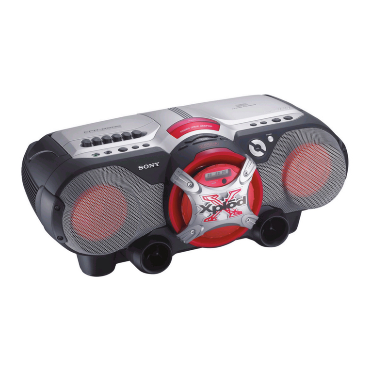
MODEL IDENTIFICATION
— BACK PANEL —
TABLE OF CONTENTS
1. SERVICE NOTE ······························································· 4
2. GENERAL ·········································································· 5
3. DISASSEMBLY ································································ 7
4. TEST MODE ···································································· 12
5. MECHANICAL ADJUSTMENTS ····························· 16
6. ELECTRICAL ADJUSTMENTS ······························· 16
7. DIAGRAMS
7-1. Circuit Board Location ····················································· 21
7-2. Block Diagrams ································································ 22
7-3. Printed Wiring Board – BD Section – ······························ 24
7-4. Schematic Diagram – BD Section – ································· 25
7-5. Printed Wiring Board – Main Section – ··························· 26
7-6. Schematic Diagram – Main (1/3) Section – ····················· 27
7-7. Schematic Diagram – Main (2/3) Section – ····················· 28
7-8. Schematic Diagram – Main (3/3) Section – ····················· 29
7-9. Printed Wiring Board – Power AMP Section –
(BX9 model) ····································································· 30
7-10. Schematic Diagram – Power AMP Section –
(BX9 model) ····································································· 31
7-11. Printed Wiring Board – Power AMP Section –
(DX9 model)····································································· 32
7-12. Schematic Diagram – Power AMP Section –
(DX9 model)····································································· 33
7-13. Printed Wiring Board – Panel Section – ··························· 34
7-14. Schematic Diagram – Panel Section – ····························· 35
7-15. Printed Wiring Board – Leaf SW Section – ···················· 36
7-16. Schematic Diagram – Leaf SW Section – ························ 37
7-17. Printed Wiring Board – Driver Section – ························· 38
7-18. Schematic Diagram – Driver Section – ···························· 39
7-19. Printed Wiring Board – Trans Section –
(BX9 model) ····································································· 40
7-20. Schematic Diagram – Trans Section –
(BX9 model) ····································································· 41
7-21. Printed Wiring Board – Trans Section –
(DX9 model)····································································· 42
7-22. Schematic Diagram – Trans Section –
(DX9 model)····································································· 43
7-23. IC Pin Function Description ············································· 44
7-24. IC Block Diagrams ··························································· 46
8. EXPLODED VIEWS
8-1. Main Section ····································································· 49
8-2. Panel Section ···································································· 50
8-3. Main Board Section ·························································· 51
8-4. Tape Mechanism Deck Section-1 ····································· 52
8-5. Tape Mechanism Deck Section-2 ····································· 53
8-6. CD Mechanism Deck Section (CDM58-K2BD38) ·········· 54
8-7. Base Unit Section (BU-K2BD38) ···································· 55
9. ELECTRICAL PARTS LIST ······································· 56
PARTS No.
• Abbreviation
AUS : Australian model
EA : Saudi Arabia model
MY : Malaysia model
SP : Singapore model
MX : Mexican model
AR : Argentina model
MODEL
BX9, DX9: MX models
DX9: E, AR, SP, MY, EA, AUS models
PARTS No.
4-225-041-4s
4-225-041-5s
Ver 1.2 2001.08

