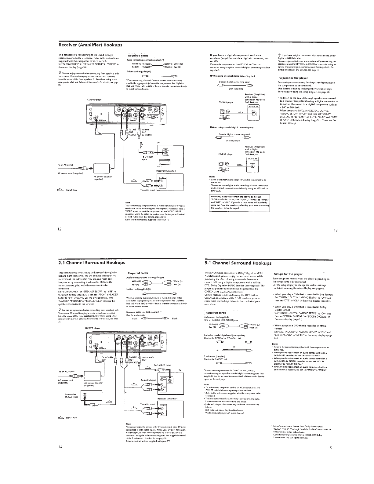
Sony DVP-F11 User manual

MICROFILM
SERVICE MANUAL
AEP Model
UK Model
E Model
Hong Kong Model
Singapore Model
Australian Model
Chinese Model
CD/DVD PLAYER
DVP-F11
RMT-D109E/D109O
SPECIFICATIONS
CD/DVD player
Laser Semiconductor laser
Signal format system PAL/(NTSC)
Audio characteristics
Frequency response DVD (PCM 96 kHz): 2 Hz to 44 kHz
(±1 dB)*
DVD (PCM 48 kHz): 2 Hz to 22 kHz
(±0.5 dB)
CD: 2 Hz to 20 kHz (±0.5 dB)
Signal-to-noise ratio More than 110 dB (LINE OUT (AUDIO
1, 2) connectors only)
Harmonic distortion Less than 0.0025%
Dynamic range More than 100 dB (DVD)
More than 97 dB (CD)
Wow and flutter Less than detected value
(±0.001% W PEAK)
Outputs and inputs
Jack Output Load impedance
type level
LINE OUT Phono 2 Vrms Over 10 kilohms
(AUDIO1, 2) jacks (at 50 kilohms)
OPTICAL Optical –18 dBm Wave length: 660 nm
output
connector
COAXIAL Phono 0.5 Vp-p 75 ohms terminated
jack
LINE OUT Phono 1.0 Vp-p 75 ohms,
(VIDEO1, 2) jacks sync negative
LINE OUT 4-pin Y: 1.0 Vp-p 75 ohms,
(S-VIDEO1, 2) mini DIN sync negative
C: 0.3 Vp-p 75 ohms terminated
(PAL)
0.286 Vp-p
(NTSC)
LINE OUT Phono 2 Vrms Over 10 kilohms
(WOOFER OUT) jacks
PHONES Phone 12 mW 32 ohms
jack
General
Power requirements DC 10.5 V
Power consumption 13 W
Dimensions (approx.) 215 ×60 ×314 mm (w/h/d)
incl. projecting parts
Mass (approx.) 2.1 kg
Operating temperature 5°C to 35°C
Operating humidity 25% to 80%
AC power adaptor
Power requirements 220 to 240 V AC, 50/60 Hz
Power consumption 19 W
Output voltage DC 10.5 V, 1.3 A in operating mode
Dimensions (approx.) 125 ×39 ×62 mm (w/h/d)
excl. projecting parts
Mass (approx.) 235 g
Operating temperature 5°C to 35°C
Storage temperature –20°C to +60°C
Supplied accessories
• Audio/Video connecting cord (1)
• S video cord (1)
• AC power adaptor AC-F11 (1)
• AC power cord (1)
• Remote commander (remote) RMT-D109O (1)
(Except Hong Kong, Singapore and Chinese)
Remote commander (remote) RMT-D109E (1)
(Hong Kong, Singapore and Chinese)
• Size AA (R6) batteries (2)
• Stand (1)
• EURO AV adaptor (1)
(Except Hong Kong, Singapore, Australian and Chinese)
* The signals from LINE OUT (AUDIO1, 2) connectors are measured.
When you play the PCM sound tracks with 96 kHz sampling frequency,
the output signals from the OPTICAL and COAXIAL connectors are
converted to 48 kHz (sampling frequency).
Design and specifications are subject to change without notice.

– 2 –
WARNING!!
WHEN SERVICING, DO NOT APPROACH THE LASER
EXIT WITH THE EYE TOO CLOSELY. IN CASE IT IS
NECESSARY TO CONFIRM LASER BEAM EMISSION,
BE SURE TO OBSERVE FROM A DISTANCE OF
MORE THAN 25 cm FROM THE SURFACE OF THE
OBJECTIVE LENS ON THE OPTICAL PICK-UP BLOCK.
CAUTION:
The use of optical instrument with this product will increase eye
hazard.
CAUTION
Use of controls or adjustments or performance of procedures
other than those specified herein may result in hazardous ra-
diation exposure.
SAFETY-RELATED COMPONENT WARNING!!
COMPONENTS IDENTIFIED BY MARK 0OR DOTTED
LINE WITH MARK 0ON THE SCHEMATIC DIAGRAMS
AND IN THE PARTS LIST ARE CRITICAL TO SAFE
OPERATION. REPLACE THESE COMPONENTS WITH
SONY PARTS WHOSE PART NUMBERS APPEAR AS
SHOWN IN THIS MANUAL OR IN SUPPLEMENTS PUB-
LISHED BY SONY.
1. Check the area of your repair for unsoldered or poorly-sol-
dered connections. Check the entire board surface for solder
splashes and bridges.
2. Check the interboard wiring to ensure that no wires are
“pinched” or contact high-wattage resistors.
3. Look for unauthorized replacement parts, particularly transis-
tors, that were installed during a previous repair. Point them
out to the customer and recommend their replacement.
SAFETY CHECK-OUT
After correcting the original service problem, perform the following
safety checks before releasing the set to the customer:
4. Look for parts which, though functioning, show obvious signs
of deterioration. Point them out to the customer and recom-
mend their replacement.
5. Check the B+ voltage to see it is at the values specified.
CLASS 3B LASER
LUOKAN 3B LASER
LASERKLASS 3B

– 3 –
Service Note ............................................................................ 4
1. GENERAL
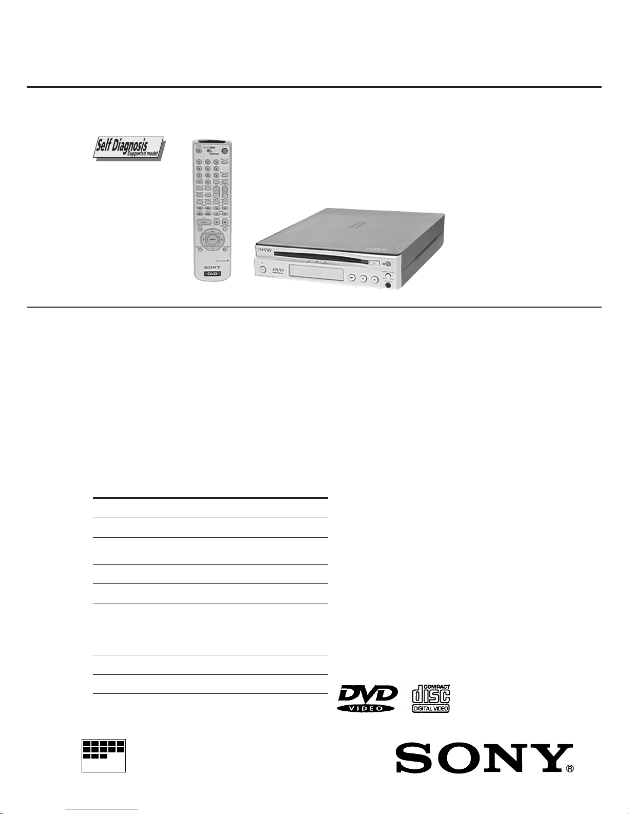
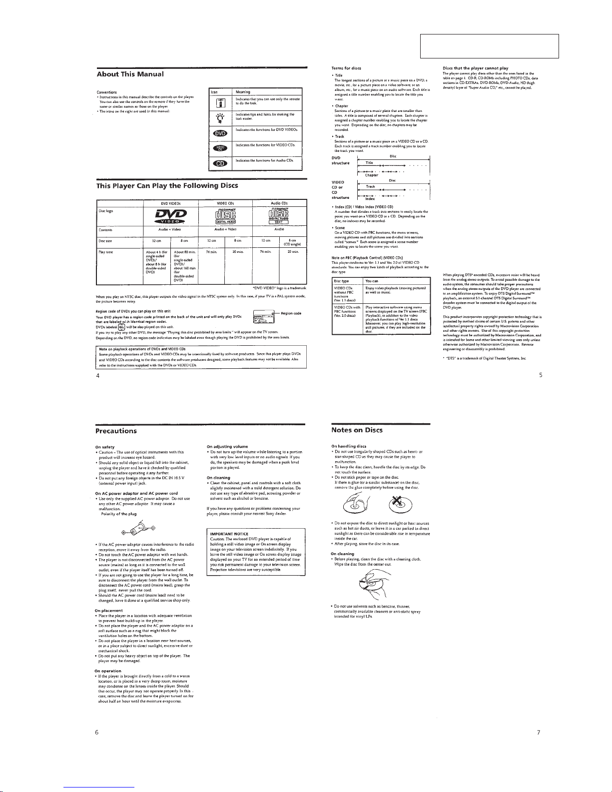
This Player Can Play the Following Discs .................... 1-1
Getting Started .............................................................. 1-2
Playing Discs ................................................................. 1-4
Using Various Functions with the Control Menu........... 1-6
Settings and Adjustments ............................................. 1-10
Index to Parts and Controls .......................................... 1-14
2. DISASSEMBLY
2-1. Case (Upper) Removal ................................................. 2-1
2-2. Chassis (Upper) Removal ............................................. 2-1
2-3. AU-222 Board Removal ................................................ 2-1
2-4. Case (Lower) Removal.................................................. 2-1
2-5. Rear Panel, MB-85 Board Removal.............................. 2-2
2-6. DC-DC Converter Unit Removal ................................... 2-2
2-7. Front Panel Section Removal........................................ 2-2
2-8. MD Block Ass’y Removal .............................................. 2-2
2-9. TK-55 Board, Optical Pick-up Removal ........................ 2-3
2-10. Chassis (Top) Block Ass’y, Chucking Arm Ass’y
Removal......................................................................... 2-3
2-11. Cam Slider, Chassis (Front) Block Ass’y Removal....... 2-3
2-12. Roller Arm Block Ass’y, LD Motor Ass’y Removal........ 2-3
2-13. Internal Views ................................................................ 2-4
2-14. Circuit Boards Location ................................................. 2-5
3. BLOCK DIAGRAMS
3-1. Overall Block Diagram................................................... 3-1
3-2. RF/Servo Block Diagram............................................... 3-3
3-3. Signal Process/Video Block Diagram ........................... 3-5
3-4. System Control Block Diagram ..................................... 3-7
3-5. Audio (1) Block Diagram ............................................... 3-9
3-6. Audio (2) Block Diagram ............................................... 3-11
3-7. Interface Control Block Diagram ................................... 3-13
3-8. Power Block Diagram .................................................... 3-15
4. PRINTED WIRING BOARDS AND SCHEMATIC
DIAGRAMS
4-1. Frame Schematic Diagram............................................ 4-3
Frame (1) Schematic Diagram ...................................... 4-3
Frame (2) Schematic Diagram ...................................... 4-5
4-2. Printed Wiring Boards and Schematic Diagrams ......... 4-7
TK-55 Printed Wiring Board .......................................... 4-7
TK-55 Schematic Diagram ............................................ 4-11
SW-332 Printed Wiring Board
and Schematic Diagram................................................ 4-13
MB-85 Printed Wiring Board ......................................... 4-15
MB-85 (AV DECODER) Schematic Diagram................ 4-19
MB-85 (SDRAM) Schematic Diagram .......................... 4-21
MB-85 (SERVO DSP) Schematic Diagram................... 4-23
MB-85 (DRIVE) Schematic Diagram ............................ 4-25
MB-85 (ARP) Schematic Diagram ................................ 4-27
MB-85 (SYSTEM CONTROL) Schematic Diagram...... 4-29
MB-85 (HGA) Schematic Diagram................................ 4-31
MB-85 (CLOCK GENERATOR/AUDIO DSP)
Schematic Diagram ....................................................... 4-33
MB-85 (DAC) Schematic Diagram ................................ 4-35
MB-85 (BIAS) Schematic Diagram ............................... 4-37
AU-222 Printed Wiring Board........................................ 4-39
AU-222 (AUDIO) Schematic Diagram........................... 4-43
AU-222 (VIDEO BUFFER) Schematic Diagram ........... 4-45
FL-111 Printed Wiring Board ........................................ 4-47
FL-111 Schematic Diagram .......................................... 4-49
FR-166 Printed Wiring Board........................................ 4-51
FR-166 Schematic Diagram.......................................... 4-53
HP-122 Printed Wiring Board
and Schematic Diagram................................................ 4-55
MPD0102 Printed Wiring Board
and Schematic Diagram................................................ 4-57
5. IC PIN FUNCTION DESCRIPTION
5-1. System Control Pin Function
(MB-85 Board IC202) .................................................... 5-1
6. TEST MODE
6-1. General Description ...................................................... 6-1
6-2. Starting Test Mode ........................................................ 6-1
6-3. Syscon Diagnosis.......................................................... 6-1
6-4. Drive Auto Adjustment .................................................. 6-5
6-5. Drive Manual Operation ................................................ 6-7
6-6. Mecha Aging ................................................................. 6-9
6-7. Emergency History........................................................ 6-9
6-8. Version Information ....................................................... 6-10
6-9. Video Level Adjustment ................................................ 6-10
6-10. If Con Self Diagnostic Function .................................... 6-11
7. ELECTRICAL ADJUSTMENTS
7-1. Power Supply Adjustment ............................................. 7-1
1. MPD0102 BOARD......................................................... 7-1
7-2. Adjustment of Video System ......................................... 7-2
1. Video Level Adjustment (MB-85 BOARD) .................... 7-2
2. S-terminal Output Check (MB-85 BOARD) .................. 7-2
3. Checking S Video Output S-C (MB-85 BOARD) .......... 7-2
7-3. Adjustment Related Parts Arrangement ....................... 7-4
8. REPAIR PARTS LIST
8-1. Exploded Views ............................................................. 8-1
8-1-1. Case and Front Panel Assemblies........................... 8-1
8-1-2. Chassis Assembly .................................................... 8-2
8-1-3. Mechanism Deck Assembly-1.................................. 8-3
8-1-4. Mechanism Deck Assembly-2.................................. 8-4
8-2. Electrical Parts List ....................................................... 8-5
TABLE OF CONTENTS
Section Title Page Section Title Page

– 4 –
SERVICE NOTE
1. DISASSEMBLY
• This set can be disassembled in the order shown below.
Roller Arm
Block Ass’y
(Page 2-3)
Set
Case (Upper)
(Page 2-1)
Chassis(Upper)
(Page 2-1)
AU-222 Board
(Page 2-1) Case (Lower)
(Page 2-1)
Case (Lower)
(Page 2-1)
Rear Panel
(Page 2-2)
MB-85 Board
(Page 2-2) DC-DC CON-
VERTER UNIT
(Page 2-2)
TK-55 Board
(Page 2-3) Chassis (Top)
Block Ass’y
(Page 2-3)
Cam Slider
(Page 2-3)
Optical
Pick-up
(Page 2-3)
MD Block
Ass’y
(Page 2-2)
Front Panel
Section
(Page 2-2)
Chassis (Front)
Ass’y
(Page 2-3)
LD Motor
Ass’y
(Page 2-3)
Chucking
Arm Ass’y
(Page 2-3)
Note on Replacing IC601 (IF CON) (FL-111 Board)
There are two types of IC601 (IF CON).
Version Type (Part No.)
Ver. 1.00 M38B57MCH-E227FP (8-759-599-87)
Ver. 1.01 M38B57MCH-D233FP (8-759-658-36)
• Version checking method
When replacing the IC601, always check the version of old part
and new part. If different, follow the “description of replacement”
given below.
Old part New part Description of replacement
(Ver.) (Ver.)
Replace as it is. (However, for the CED
Model (serial No. 800001-800100), also
1.00 replace the resistor R659 47 k (1-216-
089-00) with 1.5 k (1-216-053-00), and
1.00 further remove the resistors R653, 654,
661, 662, 663, 664.)
Replace as it is. (However, for the CED
1.01 Model (serial No. 800001-800100), also
remove the resistors R653, 654, 661,
662, 663, 664.)
1.00 Also, replace resistor R659 47 k (1-216-
1.01 089-00) with 1.5 k (1-216-053-00).
1.01 Replace as it is.
Type

1-1
SECTION 1
GENERAL This section is extracted from in-
struction manual (3-867-780-11).
DVP-F11

1-2

1-3

1-4

1-5

1-6

1-7

1-8

1-9

1-10

1-11

1-12

1-13

1-14

1-15
1-15 E

2-1
Note: Follow the disassembly procedure in the numerical order given.
2-1. CASE (UPPER) REMOVAL 2-3. AU-222 BOARD REMOVAL
2-2. CHASSIS (UPPER) REMOVAL 2-4. CASE (LOWER) REMOVAL
SECTION 2
DISASSEMBLY
DVP-F11
1Two screws
(B3)
2Remove the case (upper)
in the direction of the arrow.
4AU-222 board
1Two connectors
(CN303, 306)
5Two flat cables
(CN301, 302)
3Two screws
(B3) (ring)
2Five screws
(B3)
3Chassis (upper)
1Two screws
(B3)
2Two screws
(B3)
1Two screws
(B3)
2Four screws
(B3)
3Remove the case (lower)
in the direction of the arrow.
Other manuals for DVP-F11
3
Table of contents
Other Sony DVD Player manuals

Sony
Sony HCD-S888 User manual

Sony
Sony DVP-S300 User manual

Sony
Sony DVP-SR201P Use and maintenance manual

Sony
Sony DVP-K330 User manual

Sony
Sony DVP-S7700 User manual

Sony
Sony BDP-S495 User manual

Sony
Sony DVP-NS360 User manual

Sony
Sony DVP-NS57P - Cd/dvd Player User manual

Sony
Sony DVP-NS900V - Sacd/dvd Player User manual

Sony
Sony DVP-NC650V User manual

Sony
Sony DVP-F21 - Cd/dvd Player User manual

Sony
Sony DVP-NS705V User manual

Sony
Sony DVP-K380 User manual

Sony
Sony DVP-SR200P User manual

Sony
Sony DVP-LS755P User manual

Sony
Sony LDP-1500P User manual

Sony
Sony DVP-NS755V User manual

Sony
Sony BDP-BX38 User manual

Sony
Sony DVP-M35 User manual

Sony
Sony DVP-S525D User manual